
Integrated Silicon Solution, Inc. -- www.issi.com --
1-800-379-4774
1
ADVANCED INFORMATION
Rev. 00D
03/21/06
IS34C02B
ISSI
Æ
Copyright © 2006 Integrated Silicon Solution, Inc. All rights reserved. ISSI reserves the right to make changes to this specification and its products at any time without notice. ISSI assumes no liability
arising out of the application or use of any information, products or services described herein. Customers are advised to obtain the latest version of this device specification before relying on any published
information and before placing orders for products.
2K-bit 2-WIRE SERIAL CMOS EEPROM
with Permanent and Reversible Write-Protection
FEATURES
∑ Two-Wire Serial Interface, I
2
C
TM
compatible
≠ Bidirectional data transfer protocol
≠ 400 kHz (2.5V) and 100 KHz (1.7V) compat-
ibility
∑ Organization:
≠ 256 x 8-bit
∑ Data Protection Features
≠ Write Protect Pin
≠ Permanent Software Protection
≠ Reversible Software Protection
∑ 16-Byte Page Write Buffer
≠ Partial Page-writes permitted
∑ Low Power CMOS Technology
≠ Active Current less than 3 mA (3.6V)
≠ Standby Current less than 1 µA (1.7V)
≠ Standby Current less than 2 µA (3.6V)
∑ Low Voltage Operation
≠ IS34C02B-2: Vcc = 1.7V to 3.6V
∑ Random or Sequential Read Modes
∑ Filtered Inputs for Noise Suppression
∑ Self timed Write cycle (5ms max.)
∑ High Reliability
≠ Endurance: 1,000,000 Cycles
≠ Data Retention: 40 Years
∑ Industrial temperature range
∑ 8-pin TSSOP and DFN (leadless array)
∑ Lead-free available
ADVANCED INFORMATION
APRIL 2006
DESCRIPTION
The IS34C02B is an electrically erasable PROM device
that uses the industry-standard I
2
C communication
protocol. The IS34C02B contains a non-volatile memory
array of 2,048-bits (256K x 8 bytes), and is further
subdivided into 16 pages of 16 bytes each for Page-
write mode. The device operates over the voltage range
of 1.7V to 3.6V to satisfy the voltage requirements of
DDR2, DDR1, and many other specifications. In normal
Read or Write operations, a master device communi-
cates with the EEPROM via the two wires Serial Clock
and Serial Data. During application system boot-up, it
may be necessary to read out the contents of the
IS34C02B that pertain to the configuration of a DRAM
module. If the module manufacturer wishes to safe-
guard this memory content, the first half of the array can
be write-protected with either a permanent or reversible
software command, or the entire array can be write-
protected with the WP input pin. The IS34C02B has
three address pins, allowing up to eight devices (or
memory modules) to be uniquely accessible in a sys-
tem. To minimize board real-estate, IS34C02B is
available in two space-saving packages: TSSOP(8), and
DFN(8). All these features make the device ideal for
use as a Serial Presence Detect (SPD) EEPROM in
various types of memory modules.
2
Integrated Silicon Solution, Inc. -- www.issi.com --
1-800-379-4774
ADVANCED INFORMATION
Rev. 00D
03/21/06
IS34C02B
ISSI
Æ
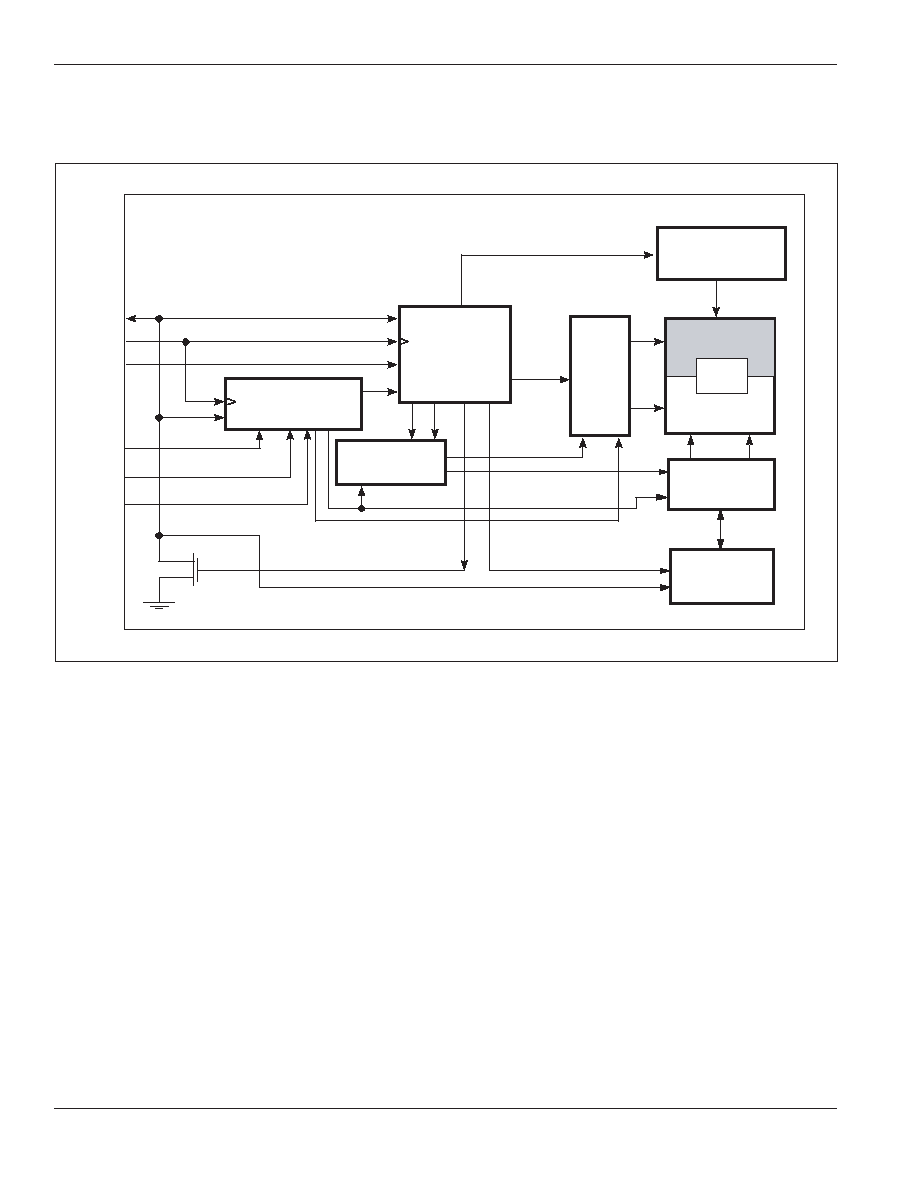
FUNCTIONAL BLOCK DIAGRAM
>
CONTROL
LOGIC
X
DECODER
SLAVE ADDRESS
REGISTER &
COMPARATOR
WORD ADDRESS
COUNTER
HIGH VOLTAGE
GENERATOR,
TIMING & CONTROL
Y
DECODER
DATA
REGISTER
Clock
DI/O
ACK
GND
WP
SCL
SDA
Vcc
nMOS
A0
A1
A2
ARRAY
80H-FFH
00H-7FH
Integrated Silicon Solution, Inc. -- www.issi.com --
1-800-379-4774
3
ADVANCED INFORMATION
Rev. 00D
03/21/06
IS34C02B
ISSI
Æ
PIN DESCRIPTIONS
A0-A2
Address Inputs
SDA
Serial Address/Data I/O
SCL
Serial Clock Input
WP
Write Protect Input
Vcc
Power Supply
GND
Ground
SCL
This input clock pin is used to synchronize the data
transfer to and from the device.
SDA
The SDA is a Bi-directional pin used to transfer addresses
and data into and out of the device. The SDA pin is an open
drain output and can be wire Or'ed with other open drain or
open collector outputs. The SDA bus
requires a pullup
resistor to Vcc.
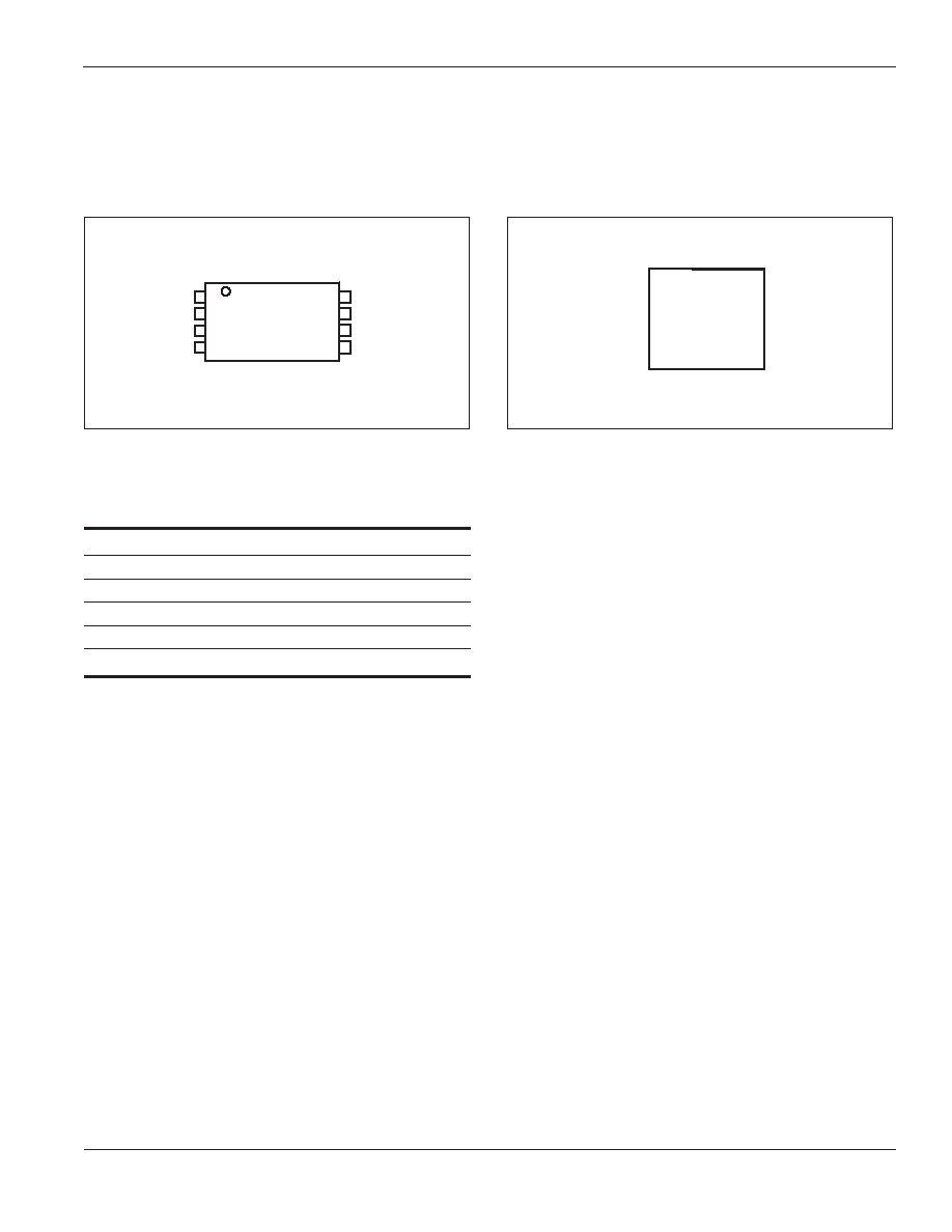
PIN CONFIGURATION
8-Pin TSSOP
WP
WP is the Write Protect pin. If the WP pin is tied to Vcc, the
entire array becomes Write Protected, and software write-
protection cannot be initiated. When WP is tied to GND or
left floating, normal read/write operations are allowed to the
device. If the device has already received a write-protection
command, the memory in the range of 00h-7Fh is read -only
regardless of the setting of the WP pin.
A0, A1, A2
The A0, A1, and A2 are the device address inputs that are
hardwired or left unconnected for hardware flexibility. When
pins are hardwired, as many as eight devices may be
addressed on a single bus system. When the pins are not
hardwired, the default values of A0, A1, and A2 are zero.
DEVICE OPERATION
The IS34C02B features a serial communication and supports
a bi-directional 2-wire bus transmission protocol called
I
2
C
TM
.
2-WIRE BUS
The two-wire bus is defined as a Serial Data line (SDA), and
a Serial Clock line (SCL). The protocol defines any device
that sends data onto the SDA bus as a transmitter, and the
receiving device as a receiver. The bus is controlled by
Master device which generates the SCL, controls the bus
access and generates the Stop and Start conditions. The
IS34C02B is the Slave device on the bus.
8-pad DFN
1
2
3
4
8
7
6
5
A0
A1
A2
GND
VCC
WP
SCL
SDA
1
2
3
4
8
7
6
5
A0
A1
A2
GND
VCC
WP
SCL
SDA
(Top View)

4
Integrated Silicon Solution, Inc. -- www.issi.com --
1-800-379-4774
ADVANCED INFORMATION
Rev. 00D
03/21/06
IS34C02B
ISSI
Æ
The Bus Protocol:
≠ Data transfer may be initiated only when the bus is not
busy
≠ During a data transfer, the SDA line must remain stable
whenever the SCL line is high. Any changes in the SDA
line while the SCL line is high will be interpreted as a
Start or Stop condition.
The state of the SDA line represents valid data after a Start
condition. The SDA line must be stable for the duration of
the High period of the clock signal. The data on the SDA
line may be changed during the Low period of the clock
signal. There is one clock pulse per bit of data. Each data
transfer is initiated with a Start condition and terminated
with a Stop condition.
Start Condition
The Start condition precedes all commands to the device
and is defined as a High to Low transition of SDA when
SCL is High. The IS34C02B monitors the SDA and SCL
lines and will not respond until the Start condition is met.
Stop Condition
The Stop condition is defined as a Low to High transition of
SDA when SCL is High. All operations must end with a Stop
condition.
Acknowledge (ACK)
After a successful data transfer, each receiving device is
required to generate an ACK. The Acknowledging device
pulls down the SDA line.
Reset
The IS34C02B contains a reset function in case the 2-
wire bus transmission is accidentally interrupted (eg. a
power loss), or needs to be terminated mid-stream. The
reset is caused when the Master device creates a Start
condition. To do this, it may be necessary for the Master
device to monitor the SDA line while cycling the SCL up
to nine times. (For each clock signal transition to High,
the Master checks for a High level on SDA.)
Standby Mode
Power consumption is reduced in standby mode. The
IS34C02B will enter standby mode: a) At Power-up, and
remain in it until SCL or SDA toggles; b) Following the Stop
signal if no write operation is initiated; or c) Following any
internal write operation
DEVICE ADDRESSING
The Master begins a transmission by sending a Start
condition. The Master then sends the address of the
particular Slave devices it is requesting. The Slave device
(Fig. 5) address is 8 bits.
The four most significant bits of the Slave device address
are fixed as 1010 for normal read/write operations, and
0110 for permanent write-protection operations.
This device has three address bits (A1, A2, and A0) that
allow up to eight IS34C02B devices to share the 2-wire
bus. Upon receiving the Slave address, the device
compares the three address bits with the hardwired A2,
A1, and A0 input pins to determine if it is the appropriate
Slave. If any of the A2 - A0 pins is neither biased to High
nor Low, internal circuitry defaults the value to Low.
The last bit of the Slave address specifies whether a Read
or Write operation is to be performed. When this bit is set
to 1, a Read operation is selected, and when set to 0, a
Write operation is selected.
After the Master transmits the Start condition and
Slave address byte (Fig. 5), the appropriate 2-wire
Slave (eg. IS34C02B) will respond with ACK on the SDA
line. The Slave will pull down the SDA on the ninth clock
cycle, signaling that it received the eight bits of data. The
selected IS34C02B then prepares for a Read or Write
operation by monitoring the bus.

Integrated Silicon Solution, Inc. -- www.issi.com --
1-800-379-4774
5
ADVANCED INFORMATION
Rev. 00D
03/21/06
IS34C02B
ISSI
Æ
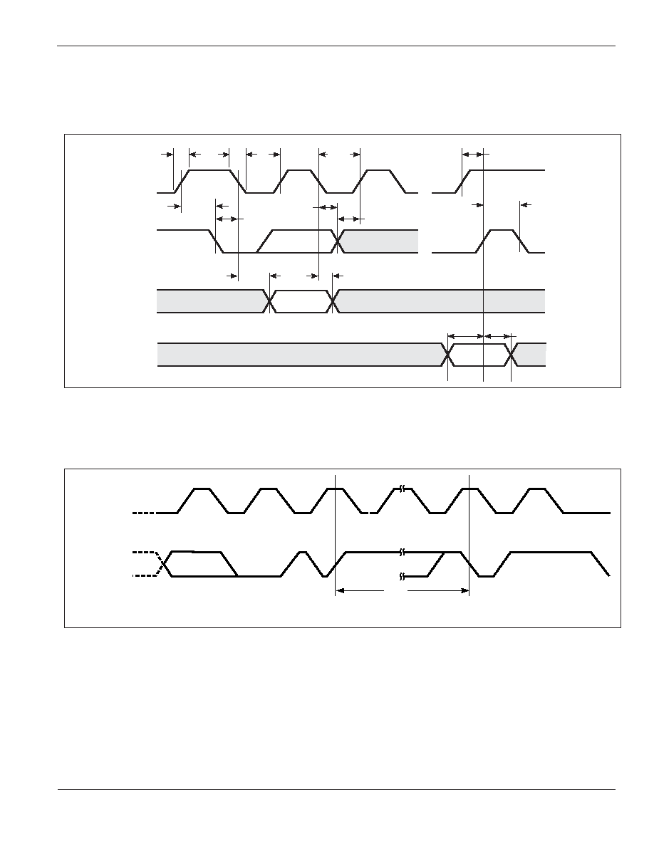
WRITE OPERATION
Byte Write
In the Byte Write mode, the Master device sends the Start
condition and the Slave address information (with the R/
W
set to Zero) to the Slave device. After the Slave generates
an ACK, the Master sends a byte address that is written into
the address pointer of the IS34C02B. After receiving another
ACK from the Slave, the Master device transmits the data
byte to be written into the address memory location. The
IS34C02B acknowledges once more and the Master
generates the Stop condition, at which time the device
begins its internal programming cycle. While this internal
cycle is in progress, the device will not respond to any
request from the Master device.
Page Write
The IS34C02B is capable of 16-byte Page-Write operation.
A Page-Write is initiated in the same manner as a Byte Write,
but instead of terminating the internal Write cycle after the
first data byte is transferred, the Master device can transmit
up to 15 more bytes. After the receipt of each data byte, the
IS34C02B responds immediately with an ACK on SDA line,
and the four lower order data byte address bits are internally
incremented by one, while the higher order bits of the data
byte address remain constant. If a byte address is
incremented from the last byte of a page, it returns to the first
byte of that page. If the Master device should transmit more
than 16 bytes prior to issuing the Stop condition, the address
counter will "roll over," and the previously written data will be
overwritten. Once all 16 bytes are received and the Stop
condition has been sent by the Master, the internal
programming cycle begins. At this point, all received data is
written to the IS34C02B in a single Write cycle. All inputs are
disabled until completion of the internal Write cycle.
Acknowledge (ACK) Polling
The disabling of the inputs can be used to take advantage
of the typical Write cycle time. Once the Stop condition is
issued to indicate the end of the host's Write operation, the
IS34C02B initiates the internal Write cycle. ACK polling can
be initiated immediately. This involves issuing the Start
condition followed by the Slave address for a Write operation.
If the IS34C02B is still busy with the Write operation, no
No Acknowledge (NoACK) will be returned. If the IS34C02B
has completed the Write operation, an ACK will be returned
and the host can then proceed with the next Read or Write
operation.
WRITE PROTECTION
Hardware Write Protection
The IS34C02B has two forms of software write protec-
tion and one form of hardware write protection. The
hardware write protection is enabled when the WP input
is held High. In this case, the entire array of the
IS34C02B is read-only regardless of the status of the
software protection. The hardware protection is disabled
when the WP input is held Low or is floating. In this
case, the upper half of the array (80h-FFh) can be
modified by a valid Write command, and the lower half of
the array (
00h-7Fh
) can be modified only if software write
protection has not been enabled.
Reversible Software Write Protection
There is a non-volatile flag for each of the two forms of
software write protection. When the bit value for either
flag or both flags is 1, it is not possible to modify the
contents of the lower 128 bytes of the array (
00h-7Fh
). If
the bit value for both flags is 0, it is possible to modify
this half of the array with a valid Write command,
assuming WP is held Low or is floating. The device is
shipped with both flags cleared. One of those flags is
the Reversible Software Write Protection (RSWP) flag,
and can be changed with the Set RSWP and Clear
RSWP commands. The flag can also be verified without
being changed with a Read SWP command. In order to
set, clear or read the RSWP, the IS34C02B input pins
must be as follows: A0 must be held to an extra high
voltage of VHV (see DC Characteristics), while A2 and
A1 must be set High, Low, or left floating, depending on
the desired command (see Figure 5). Once these input
conditions are met, a command can be issued to the
device.
The reversible software commands are initiated similarly
to a normal byte write operation; however, the slave
device address begins with the bit values 0110. The
next three bits are A2 = 0, A1 = 0 or 1, and A0 = 1, so
that they logically match the values on the input pins. If
the last bit of the slave device address (R/
W) is 0, the
RSWP flag can be Cleared or Set. If R/
W is 1, the flag
can be verified with the Read SWP command. Following
this bit, the device responds with either ACK or NoACK,
depending on the exact command and the flag status
(see Table 1: Reversible Instructions). To complete the

6
Integrated Silicon Solution, Inc. -- www.issi.com --
1-800-379-4774
ADVANCED INFORMATION
Rev. 00D
03/21/06
IS34C02B
ISSI
Æ
Set RSWP or Clear RSWP command, the Master must
transmit a dummy address byte, a dummy data byte,
and a Stop signal. To actually modify the RSWP flag,
WP should be held Low or be floating during entire
command sequence. Before resuming any other
command, the internal write cycle time should be
observed. To complete the Read SWP Status or Read
CWP Status command, the Master can transmit a Stop
signal after the ACK/NoACK. The WP input is not
evaluated for the Read SWP Status or Read CSP
Status commands.
Permanent Software Write Protection
The IS34C02B contains a permanent software write
protection (PSWP) feature. If the non-volatile PSWP flag
has a bit value of 1, the array region of 00h-7Fh is
protected from modification. If the PSWP flag has a bit
value of 0, the write protection for the lower half of the
array is determined solely by the statuses of RSWP and
the WP input. After the PSWP flag is set to 1 via the
Permanent Write Protect command, the protected area
becomes irreversibly read-only despite power removal
and re-application on the device. Once enabled, the
permanent protection is independent of the status of the
WP pin.
The Permanent Software Write Protect command is
initiated similarly to a normal byte write operation;
however, the slave device address begins with the bit
values of 0110 (see Figure 5). The following three bits
are A2-A0
, so that they logically match the values on
the input pins
. The last bit of the slave address (R/
W) is
0. The IS34C02B
responds with either ACK or NoACK,
depending on the flag status (see Table 1: Permanent
Instructions). Assuming an ACK is received,
Master
then must complete the sequence by transmitting a
dummy address byte, dummy data byte, and a Stop
signal (see Figure 11). The WP pin should be held Low
or left floating during the entire command. Before
resuming any other command, the internal write cycle
should be observed.
The status of the PSWP can be safely determined
without any changes by transmitting the same slave
address as above, but with the last bit (R/
W) set to 1
(see Figure 12). If the PSWP has been set, the
IS34C02B will not acknowledge any slave address
starting with bits 0110 (see Figure 5).
To complete the
command, the Master can transmit a Stop signal after
the ACK/NoACK.

Integrated Silicon Solution, Inc. -- www.issi.com --
1-800-379-4774
7
ADVANCED INFORMATION
Rev. 00D
03/21/06
IS34C02B
ISSI
Æ
TABLE 1
Normal Instructions
Command
PSWP
RSWP
WP
1
ACK
Address
ACK
Data Byte
Data Byte
Write
(Permanent)
(Reversible)
Command
Address
ACK
Cycle
Read
X
X
X
ACK
00h-FFh
ACK
Data Byte
ACK
No
Write
0
0
0
ACK
00h-FFh
ACK
Data Byte
ACK
Yes
Write
X
X
1
ACK
00h-FFh
ACK
Data Byte
ACK
No
Write
1
X
X
ACK
00h-7Fh
ACK
Data Byte
ACK
No
Write
X
1
X
ACK
00h-7Fh
ACK
Data Byte
ACK
No
Write
X
X
0
ACK
80h-FFh
ACK
Data Byte
ACK
Yes
Permanent Instructions
Command
PSWP
RSWP
WP
1
ACK
Address
ACK
Data Byte
Data Byte
Write
(Permanent)
(Reversible)
Command
Address
ACK
Cycle
Read PSWP Status
4
0
X
X
ACK
Dummy
ACK
Dummy
ACK
No
Address
Byte
Read PSWP Status
1
X
X
NoACK
--
--
--
--
No
Set PSWP
0
X
0
ACK
Dummy
ACK
Dummy
ACK
Yes
Address
Byte
Set PSWP
1
X
0
NoACK
--
--
--
--
No
Set PSWP
0
X
1
ACK
Dummy
ACK
Dummy
ACK
No
Address
Byte
Set PSWP
1
X
1
NoACK
--
--
--
--
No
Reversible Instructions
Command
PSWP
RSWP
WP
1
ACK
Address
ACK
Data Byte
Data Byte
Write
(Permanent)
(Reversible)
Command
Address
ACK
Cycle
Read SWP Status
4
X
0
X
ACK
Dummy
ACK
Dummy
ACK
No
Address
Byte
Read SWP Status
X
1
X
NoACK
--
--
--
--
No
Read CWP Status
3,4
0
X
X
ACK
Dummy
ACK
Dummy
ACK
No
Address
Byte
Read CWP Status
3
1
X
X
NoACK
--
--
--
--
No
Set RSWP
X
0
0
ACK
Dummy
ACK
Dummy
ACK
Yes
Address
Byte
Set RSWP
X
1
0
NoACK
--
--
--
--
No
Set RSWP
X
0
1
ACK
Dummy
ACK
Dummy
ACK
No
Address
Byte
Set RSWP
X
1
1
NoACK
--
--
--
--
No
Clear RSWP
0
X
0
ACK
Dummy
ACK
Dummy
ACK
Yes
Address
Byte
Clear RSWP
1
X
0
NoACK
--
--
--
--
No
Clear RSWP
0
X
1
ACK
Dummy
ACK
Dummy
ACK
No
Address
Byte
Clear RSWP
1
X
1
NoACK
--
--
--
--
No
Notes:
1. WP = 1 if input level is High. WP = 0 if input level is GND or floating.
2. X = Don't Care.
3. Read CWP Status yields the same result as Read PSWP Status.
4. Read out Don't Care Dummy Address and Dummy Data is optional.

8
Integrated Silicon Solution, Inc. -- www.issi.com --
1-800-379-4774
ADVANCED INFORMATION
Rev. 00D
03/21/06
IS34C02B
ISSI
Æ
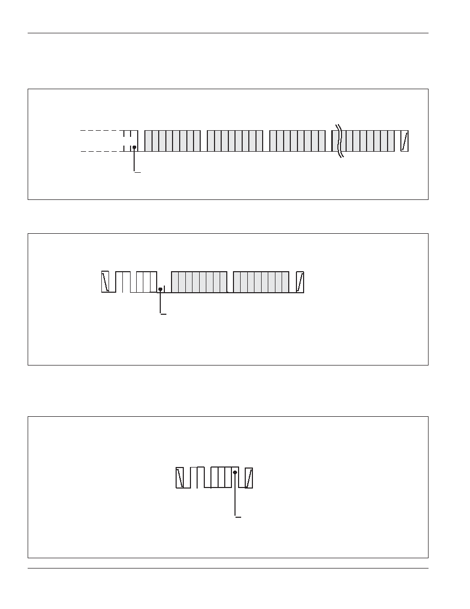
Sequential Read
Sequential Reads can be initiated as either a Current
Address Read or Random Address Read. After the
IS34C02B sends the initial byte sequence, the Master
device responds with an ACK indicating it requires additional
data from the IS34C02B. The IS34C02B continues to output
data for each ACK received. The Master device terminates
the sequential Read operation by pulling SDA High (no ACK)
indicating the last data byte to be read, followed by a Stop
condition.
The data output is sequential, with the data from address n
followed by the data from address n+1, ... etc. The address
counter increments by one automatically, allowing the
entire memory contents to be serially read during sequential
Read operations. When the memory address boundary 255
is reached, the address counter "rolls over" to address 0, and
the IS34C02B continues to output data for each ACK
received. (Refer to Figure 10. Sequential Read Operation
Starting with a Random Address Read Diagram.)
READ OPERATION
Read operations are initiated in the same manner as Write
operations, except that the (R/
W) bit of the Slave address is
set to "1". There are three Read operation options: current
address read, random address read and sequential read.
Current Address Read
The IS34C02B contains an internal address counter
which maintains the address of the last byte accessed,
incremented by one. For example, if the previous
operation is either a Read or Write operation addressed
to the address location n, the internal address counter
would increment to address location n+1. When the
IS34C02B receives the Device Addressing Byte with a
Read operation (R/
W bit set to "1"), it will respond an ACK
and transmit the 8-bit data byte stored at address
location n+1. The Master should not acknowledge the
transfer but should generate a Stop condition so the
IS34C02B discontinues transmission. If the last byte of
the memory was the previous access, the data from
location '0' will be transmitted. (Refer to Figure 8.
Current Address Read Diagram.)
Random Address Read
Selective Read operations allow the Master device to select
at random any memory location for a Read operation. The
Master device first performs a 'dummy' Write operation by
sending the Start condition, Slave address and word address
of the location it wishes to read. After the IS34C02B
acknowledges the word address, the Master device resends
the Start condition and the Slave address, this time with the
R/
W bit set to one. The IS34C02B then responds with its
ACK and sends the data requested. The Master device
does not send an ACK but will generate a Stop
condition. (Refer to Figure 9. Random Address Read
Diagram.)
Integrated Silicon Solution, Inc. -- www.issi.com --
1-800-379-4774
9
ADVANCED INFORMATION
Rev. 00D
03/21/06
IS34C02B
ISSI
Æ
SCL
SDA
Master
Transmitter/
Receiver
IS34C02B
Vcc
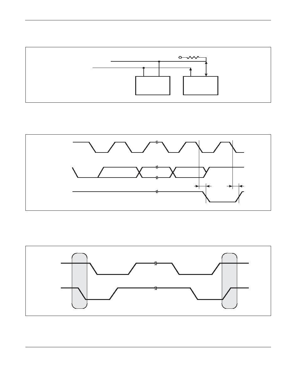
Figure 1. Typical System Bus Configuration
t
AA
Data Output
from
Transmitter
SCL from
Master
Data Output
from
Receiver
1
8
9
ACK
t
AA
Figure 2. Output Acknowledge
STOP
Condition
SCL
SDA
START
Condition
Figure 3. Start and Stop Conditions
10
Integrated Silicon Solution, Inc. -- www.issi.com --
1-800-379-4774
ADVANCED INFORMATION
Rev. 00D
03/21/06
IS34C02B
ISSI
Æ
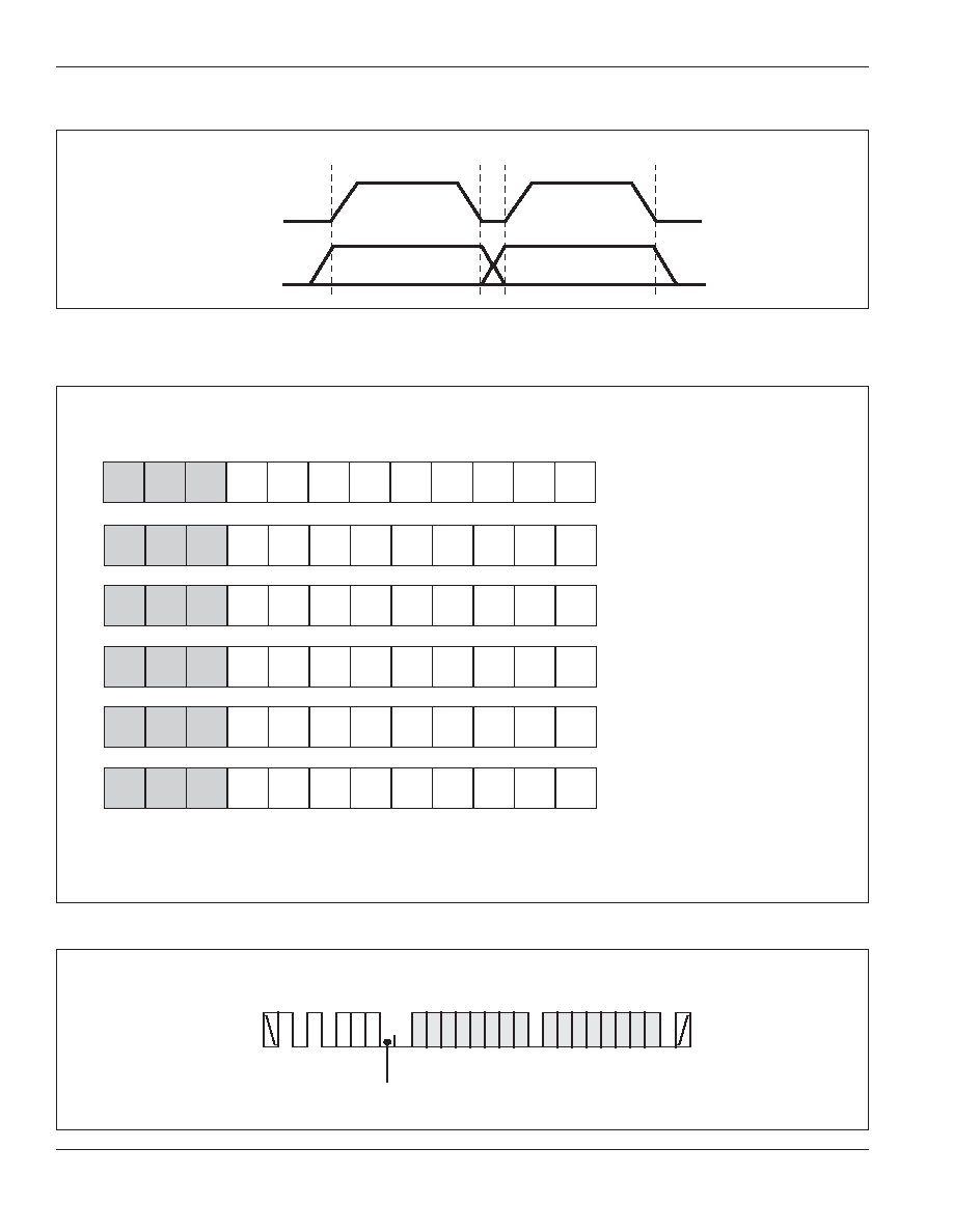
Figure 5. Command Configuration
Figure 4. Data Validity Protocol
SCL
SDA
Data Stable
Data Stable
Data Change
Figure 6. Byte Write
SDA
Bus
Activity
S
T
A
R
T
M
S
B
L
S
B
M
S
B
W
R
I
T
E
S
T
O
P
R/
W
A
C
K
A
C
K
A
C
K
Data
Device
Address
Word Address
*
*
*
*
Acknowledges provided by the slave regardless of hardware or software Write Protection.
7
BIT
4
3
1
2
5
6
0
R/
W
A0
A1
A2
0
1
0
1
Normal
Instruction
2
R/
W
A0
A1
A2
0
1
0
1
Permanent Write
Protection Instruction
2
Pin Connection
1
Slave Device Address
A2
A2
A1
A0
A2
A1
A0
0
1
0
0
0
1
0
1
Set Write Protection
(SWP)
GND GND
V
HV
0
1
1
0
0
1
0
1
Clear Write Protection
(CWP)
GND
Vcc
V
HV
1
1
0
0
0
1
0
1
Read SWP
GND GND
V
HV
1
1
1
0
0
1
0
1
Read CWP
GND
Vcc
V
HV
A1
A0
Note:
1. A2-A0 input pin connections must be GND (or floating), Vcc, or V
HV
.
2. Bits 1, 2, and 3 of the device address will be compared with the values on the external pins.
Integrated Silicon Solution, Inc. -- www.issi.com --
1-800-379-4774
11
ADVANCED INFORMATION
Rev. 00D
03/21/06
IS34C02B
ISSI
Æ
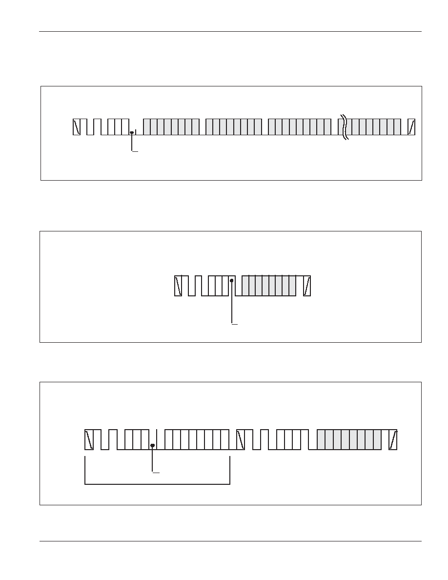
Figure 8. Current Address Read
Figure 9. Random Address Read
SDA
Bus
Activity
S
T
A
R
T
M
S
B
L
S
B
N
O
A
C
K
R
E
A
D
S
T
O
P
A
C
K
Data
Device
Address
R/W
SDA
Bus
Activity
A
C
K
A
C
K
A
C
K
Data n
Word
Address (n)
Device
Address
DUMMY WRITE
Device
Address
S
T
A
R
T
W
R
I
T
E
R
E
A
D
S
T
A
R
T
S
T
O
P
M
S
B
L
S
B
N
O
A
C
K
R/W
Figure 7. Page Write
SDA
Bus
Activity
S
T
A
R
T
M
S
B
L
S
B
W
R
I
T
E
A
C
K
A
C
K
A
C
K
A
C
K
Data (n+1)
Data (n)
Word Address (n)
Device
Address
S
T
O
P
A
C
K
Data (n+15)
R/W
*
*
*
*
*
*
Acknowledges provided by the slave regardless of hardware or software Write Protection.
12
Integrated Silicon Solution, Inc. -- www.issi.com --
1-800-379-4774
ADVANCED INFORMATION
Rev. 00D
03/21/06
IS34C02B
ISSI
Æ
Figure 11. SET PERMANENT WRITE PROTECTION
Figure 12. READ PERMANENT WRITE PROTECTION
SDA
Bus
Activity
S
T
A
R
T
M
S
B
L
S
B
R
E
A
D
A
C
K
Device
Address
R/W
S
T
O
P
*
* The slave does not provide an acknowledgement if the permanent write protection is already enabled.
SDA
Bus
Activity
S
T
A
R
T
M
S
B
L
S
B
M
S
B
W
R
I
T
E
S
T
O
P
R/W
A
C
K
A
C
K
A
C
K
Data
Device
Address
Word Address
*
* The slave does not provide an acknowledgement if the permanent write protection is already enabled.
# # # # # # # #
# # # # # # # #
# Don't care bits are required.
Figure 10. Sequential Read
S
T
O
P
N
O
A
C
K
A
C
K
A
C
K
A
C
K
A
C
K
Data Byte n+X
Data Byte n+1
Data Byte n
Data Byte n+2
R/W
SDA
Bus
Activity
Device
Address
R
E
A
D

Integrated Silicon Solution, Inc. -- www.issi.com --
1-800-379-4774
13
ADVANCED INFORMATION
Rev. 00D
03/21/06
IS34C02B
ISSI
Æ
ABSOLUTE MAXIMUM RATINGS
(1)
Symbol
Parameter
Value
Unit
V
S
Supply Voltage
≠0.5 to +6.5
V
V
P
Voltage on Any Pin
≠0.5 to Vcc + 0.5
V
T
BIAS
Temperature Under Bias
≠55 to +125
∞C
T
STG
Storage Temperature
≠65 to +150
∞C
I
OUT
Output Current
5
mA
Notes:
1. Stress greater than those listed under ABSOLUTE MAXIMUM RATINGS may cause
permanent damage to the device. This is a stress rating only and functional operation
of the device at these or any other conditions above those indicated in the operational
sections of this specification is not implied. Exposure to absolute maximum rating
conditions for extended periods may affect reliability.
OPERATING RANGE
(IS34C02B-2)
Range
Ambient Temperature
V
CC
Industrial
≠40∞C to +85∞C
1.7V to 3.6V
CAPACITANCE
(1,2)
Symbol
Parameter
Conditions
Max.
Unit
C
IN
Input Capacitance
V
IN
= 0V
6
pF
C
OUT
Output Capacitance
V
OUT
= 0V
8
pF
Notes:
1. Tested initially and after any design or process changes that may affect these parameters.
2. Test conditions: T
A
= 25∞C, f = 400 KHz, Vcc = 3.0V.

14
Integrated Silicon Solution, Inc. -- www.issi.com --
1-800-379-4774
ADVANCED INFORMATION
Rev. 00D
03/21/06
IS34C02B
ISSI
Æ
DC ELECTRICAL CHARACTERISTICS
Industrial (T
A
= -40
o
C to +85
o
C)
Symbol
Parameter
Test Conditions
Min.
Max.
Unit
V
OL
1
Output Low Voltage
V
CC
= 1.7V, I
OL
= 0.15 mA
--
0.2
V
V
OL
2
Output Low Voltage
V
CC
= 3.6V, I
OL
= 2.1 mA
--
0.4
V
V
IH
Input High Voltage
V
CC
X
0.7 V
CC
+ 0.5
V
V
IL
Input Low Voltage
≠1.0
V
CC
X
0.3
V
V
HV
A0 High Voltage
V
HV
- V
CC
> 4.8V
7
10
V
I
LI
Input Leakage Current
V
IN
= V
CC
max.
--
3
µA
I
LO
Output Leakage Current
--
3
µA
AC ELECTRICAL CHARACTERISTICS
Industrial (T
A
= -40
o
C to +85
o
C)
1.7V
Vcc < 2.2V 2.2V
Vcc
3.6V
Symbol
Parameter
Min.
Max.
Min.
Max.
Unit
f
SCL
SCL Clock Frequency
0
100
0
400
KHz
T
Noise Suppression Time
(1)
--
100
--
50
ns
t
Low
Clock Low Period
4.7
--
1.2
--
µs
t
High
Clock High Period
4
--
0.6
--
µs
t
BUF
Bus Free Time Before New Transmission
(1)
4.7
--
1.2
--
µs
t
SU:STA
Start Condition Setup Time
4
--
0.6
--
µs
t
SU:STO
Stop Condition Setup Time
4
--
0.6
--
µs
t
HD:STA
Start Condition Hold Time
4
--
0.6
--
µs
t
HD:STO
Stop Condition Hold Time
4
--
0.6
--
µs
t
SU:DAT
Data In Setup Time
100
--
100
--
ns
t
HD:DAT
Data In Hold Time
0
--
0
--
ns
t
SU
:
WP
WP pin Setup Time
4
--
0.6
--
µs
t
HD
:
WP
WP pin Hold Time
4.7
--
1.2
--
µs
t
DH
Data Out Hold Time (SCL Low to SDA Data Out Change)
100
--
50
--
ns
t
AA
Clock to Output (SCL Low to SDA Data Out Valid)
100
3500
50
900
ns
t
R
SCL and SDA Rise Time
(1)
--
1000
--
300
ns
t
F
SCL and SDA Fall Time
(1)
--
300
--
300
ns
t
WR
Write Cycle Time
--
5
--
5
ms
POWER SUPPLY CHARACTERISTICS
Industrial (T
A
= -40
o
C to +85
o
C)
Symbol
Parameter
Test Conditions
Min.
Max.
Unit
I
CC
1
Vcc Operating Current
Read at 100 KHz (Vcc = 3.6V)
--
1.0
mA
I
CC
2
Vcc Operating Current
Write at 100 KHz (Vcc = 3.6V)
--
3.0
mA
I
SB
1
Standby Current
Vcc = 1.7V
--
1
µA
I
SB
2
Standby Current
Vcc = 3.6V
--
2
µA
Notes: V
IL
min and V
IH
max are reference only and are not tested.
Note:
1. These parameters are characterized, but not 100% tested.
Integrated Silicon Solution, Inc. -- www.issi.com --
1-800-379-4774
15
ADVANCED INFORMATION
Rev. 00D
03/21/06
IS34C02B
ISSI
Æ
8th BIT
ACK
WORD n
STOP
Condition
START
Condition
t
WR
SCL
SDA
FIGURE 14. WRITE CYCLE TIMING
FIGURE 13. AC WAVEFORMS
t
SU:STA
t
F
t
HIGH
t
LOW
t
R
t
SU:STO
t
BUF
t
DH
t
AA
t
HD:STA
t
HD:DAT
t
SU:DAT
SCL
SDA
IN
SDA
OUT
t
SU:WP
t
HD:WP
WP

16
Integrated Silicon Solution, Inc. -- www.issi.com --
1-800-379-4774
ADVANCED INFORMATION
Rev. 00D
03/21/06
IS34C02B
ISSI
Æ
ORDERING INFORMATION
Industrial Range: -40∞C to +85∞C, Lead-free
Voltage
Range
Part Number
Package
1.7V
IS34C02B-2DLI
DFN
to 3.6V
IS34C02B-2ZLI
TSSOP
PACKAGING INFORMATION
ISSI
Æ
Integrated Silicon Solution, Inc. -- www.issi.com --
1-800-379-4774
Rev. B
02/13/06
Copyright © 2006 Integrated Silicon Solution, Inc. All rights reserved. ISSI reserves the right to make changes to this specification and its products at any time
without notice. ISSI assumes no liability arising out of the application or use of any information, products or services described herein. Customers are advised to
obtain the latest version of this device specification before relying on any published information and before placing orders for products.
Dual Flat No-Lead
Package Code: D (8-pad)
A2
b
(8X)
(8X)
A1
A1
A3
D
E
A
L (8X)
L (8X)
e (6X)
e (6X)
1.50 REF.
1.50 REF.
D2
E2
E2
Pad 1 ID
Pad 1 index area
tie bars
(3)
Notes:
1. Refer to JEDEC Drawing MO-229.
2. This is the metallized terminal and
is measured between 0.18 mm
and 0.30 mm from the terminal tip.
The terminal may have a straight
end instead of rounded.
3. Package may have exposed tie
bars, ending flush with package
edge.
DFN
MILLIMETERS
Sym.
Min. Nom. Max.
N0.
Pad
8
D
2.00 BSC
E
3.00 BSC
D2
1.50
--
1.75
E2
1.60
--
1.90
A
0.70
0.75
0.80
A1
0.0
0.02
0.05
A2
--
--
0.75
A3
0.20 REF
L
0.30
0.40
0.50
e
0.50 BSC
b
0.18
0.25
0.30
Integrated Silicon Solution, Inc.
PACKAGING INFORMATION
ISSI
Æ
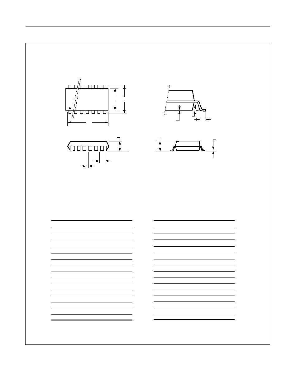
Thin Shrink Small Outline TSSOP
Package Code: Z (8 pin, 14 pin)
Rev B 02/01/02
TSSOP (Z)
Ref. Std.
JEDEC MO-153
No. Leads
8
Millimeters
Inches
Symbol Min
Max
Min
Max
A
--
1.20
--
0.047
A1
0.05
0.15
0.002 0.006
A2
0.80
1.05
0.032 0.041
B
0.19
0.30
0.007 0.012
C
0.09
0.20
0.004 0.008
D
2.90
3.10
0.114 0.122
E1
4.30
4.50
0.169 0.177
E
6.40 BSC
0.252 BSC
e
0.65 BSC
0.026 BSC
L
0.45
0.75
0.018 0.030
--
8∞
--
8∞
TSSOP (Z)
Ref. Std.
JEDEC MO-153
No. Leads
14
Millimeters
Inches
Symbol Min
Max
Min
Max
A
--
1.20
--
0.047
A1
0.05
0.15
0.002
0.006
A2
0.80
1.05
0.031
0.041
B
0.19
0.30
0.007
0.012
C
0.09
0.20
0.0035 0.008
D
4.90
5.10
0.193
0.201
E1
4.30
4.50
0.170
0.177
E
6.40 BSC
0.252 BSC
e
0.65 BSC
0.026 BSC
L
0.45
0.75
0.0177 0.0295
--
8∞
--
8∞
D
B
e
E1
A2
E
C
A
A1
L
1
N
N/2
SSI reserves the right to make changes to its products at any time without notice in order to improve design and supply the best possible product. We assume no responsibility for any errors which may
appear in this publication. © Copyright 2002, Integrated Silicon Solution, Inc.