Integrated Silicon Solution, Inc. -- 1-800-379-4774
1
Rev. B
04/28/05
IS41C16256A
IS41LV16256A
ISSI
Æ
Copyright © 2005 Integrated Silicon Solution, Inc. All rights reserved. ISSI reserves the right to make changes to this specification and its products at any time
without notice. ISSI assumes no liability arising out of the application or use of any information, products or services described herein. Customers are advised to
obtain the latest version of this device specification before relying on any published information and before placing orders for products.
FEATURES
∑ TTL compatible inputs and outputs
∑ Refresh Interval: 512 cycles/8 ms
∑ Refresh Mode :
RAS
-Only,
CAS
-before-
RAS
(CBR),
and Hidden
∑ JEDEC standard pinout
∑ Single power supply
5V ± 10% (IS41C16256A)
3.3V ± 10% (IS41LV16256A)
∑ Byte Write and Byte Read operation via two
CAS
∑ Lead-free available
DESCRIPTION
The
ISSI
IS41C16256A and IS41LV16256A are 262,144 x 16-
bit high-performance CMOS Dynamic Random Access
Memory. Both products offer accelerated cycle access EDO
Page Mode. EDO Page Mode allows 512 random accesses
within a single row with access cycle time as short as 10ns per
16-bit word. The Byte Write control, of upper and lower byte,
makes the IS41C16256A and IS41LV16256A ideal for use in
16 and 32-bit wide data bus systems.
These features make the IS41C16256A and IS41LV1626 ide-
ally suited for high band-width graphics, digital signal pro-
cessing, high-performance computing systems, and peripheral
applications.
The IS41C16256A and IS41LV16256A are packaged in 40-
pin 400-mil SOJ and TSOP (Type II).
256K x 16
(4-MBIT) DYNAMIC RAM
APRIL 2005
WITH EDO PAGE MODE
KEY TIMING PARAMETERS
Parameter
-35
-60
Unit
Max.
RAS
Access Time (t
RAC
)
35
60
ns
Max.
CAS
Access Time (t
CAC
)
11
15
ns
Max. Column Address Access Time (t
AA
)
18
30
ns
Min. EDO Page Mode Cycle Time (t
PC
)
14
25
ns
Min. Read/Write Cycle Time (t
RC
)
60
110
ns
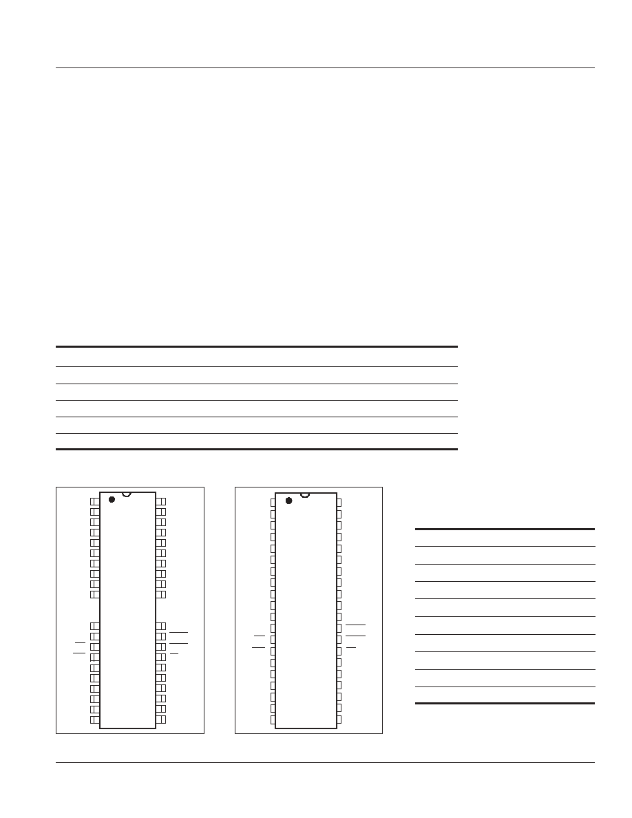
PIN CONFIGURATIONS
40-Pin TSOP (Type II)
40-Pin SOJ
PIN DESCRIPTIONS
A0-A8
Address Inputs
I/O0-15
Data Inputs/Outputs
WE
Write Enable
OE
Output Enable
RAS
Row Address Strobe
UCAS
Upper Column Address Strobe
LCAS
Lower Column Address Strobe
Vcc
Power
GND
Ground
NC
No Connection
1
2
3
4
5
6
7
8
9
10
11
12
13
14
15
16
17
18
19
20
40
39
38
37
36
35
34
33
32
31
30
29
28
27
26
25
24
23
22
21
VCC
I/O0
I/O1
I/O2
I/O3
VCC
I/O4
I/O5
I/O6
I/O7
NC
NC
WE
RAS
NC
A0
A1
A2
A3
VCC
GND
I/O15
I/O14
I/O13
I/O12
GND
I/O11
I/O10
I/O9
I/O8
NC
LCAS
UCAS
OE
A8
A7
A6
A5
A4
GND
1
2
3
4
5
6
7
8
9
10
11
12
13
14
15
16
17
18
19
20
40
39
38
37
36
35
34
33
32
31
30
29
28
27
26
25
24
23
22
21
VCC
I/O0
I/O1
I/O2
I/O3
VCC
I/O4
I/O5
I/O6
I/O7
NC
NC
WE
RAS
NC
A0
A1
A2
A3
VCC
GND
I/O15
I/O14
I/O13
I/O12
GND
I/O11
I/O10
I/O9
I/O8
NC
LCAS
UCAS
OE
A8
A7
A6
A5
A4
GND

4
Integrated Silicon Solution, Inc. -- 1-800-379-4774
Rev. B
04/28/05
IS41C16256A
IS41LV16256A
ISSI
Æ
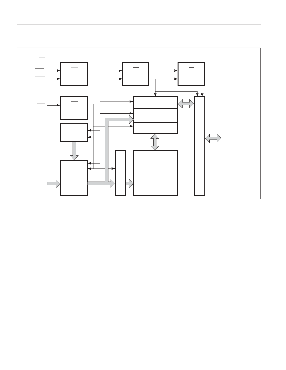
Functional Description
The IS41C16256A and IS41LV16256A is a CMOS DRAM
optimized for high-speed bandwidth, low power applica-
tions. During READ or WRITE cycles, each bit is uniquely
addressed through the 18 address bits. These are en-
tered nine bits (A0-A8) at a time. The row address is
latched by the Row Address Strobe (
RAS
). The column
address is latched by the Column Address Strobe (
CAS
).
RAS
is used to latch the first nine bits and
CAS
is used the
latter nine bits.
The IS41C16256A and IS41LV16256A has two
CAS
con-
trols,
LCAS
and
UCAS
. The
LCAS
and
UCAS
inputs
internally generates a
CAS
signal functioning in an iden-
tical manner to the single
CAS
input on the other 256K x
16 DRAMs. The key difference is that each
CAS
controls
its corresponding I/O tristate logic (in conjunction with
OE
and
WE
and
RAS
).
LCAS
controls I/O0 through I/O7 and
UCAS
controls I/O8 through I/O15.
The IS41C16256A and IS41LV16256A
CAS
function is
determined by the first
CAS
(
LCAS
or
UCAS
) transitioning
LOW and the last transitioning back HIGH. The two
CAS
controls give the IS41C16256A both BYTE READ and
BYTE WRITE cycle capabilities.
Memory Cycle
A memory cycle is initiated by bring
RAS
LOW and it is
terminated by returning both
RAS
and
CAS
HIGH. To
ensures proper device operation and data integrity any
memory cycle, once initiated, must not be ended or
aborted before the minimum t
RAS
time has expired. A new
cycle must not be initiated until the minimum precharge
time t
RP
, t
CP
has elapsed.
Read Cycle
A read cycle is initiated by the falling edge of
CAS
or
OE
,
whichever occurs last, while holding
WE
HIGH. The
column address must be held for a minimum time speci-
fied by t
AR
. Data Out becomes valid only when t
RAC
, t
AA
,
t
CAC
and t
OEA
are all satisfied. As a result, the access time
is dependent on the timing relationships between these
parameters.
Write Cycle
A write cycle is initiated by the falling edge of
CAS
and
WE
, whichever occurs last. The input data must be valid
at or before the falling edge of
CAS
or
WE
, whichever
occurs last.
Refresh Cycle
To retain data, 512 refresh cycles are required in each
8 ms period. There are two ways to refresh the memory.
1. By clocking each of the 512 row addresses (A0 through
A8) with
RAS
at least once every 8 ms. Any read, write,
read-modify-write or
RAS
-only cycle refreshes the ad-
dressed row.
2. Using a
CAS
-before-
RAS
refresh cycle.
CAS
-before-
RAS
refresh is activated by the falling edge of
RAS
,
while holding
CAS
LOW. In
CAS
-before-
RAS
refresh
cycle, an internal 9-bit counter provides the row ad-
dresses and the external address inputs are ignored.
CAS
-before-
RAS
is a refresh-only mode and no data
access or device selection is allowed. Thus, the output
remains in the High-Z state during the cycle.
Extended Data Out Page Mode
EDO page mode operation permits all 512 columns within
a selected row to be randomly accessed at a high data
rate.
In EDO page mode read cycle, the data-out is held to the
next
CAS
cycle's falling edge, instead of the rising edge.
For this reason, the valid data output time in EDO page
mode is extended compared with the fast page mode. In
the fast page mode, the valid data output time becomes
shorter as the
CAS
cycle time becomes shorter. There-
fore, in EDO page mode, the timing margin in read cycle
is larger than that of the fast page mode even if the
CAS
cycle time becomes shorter.
In EDO page mode, due to the extended data function, the
CAS
cycle time can be shorter than in the fast page mode
if the timing margin is the same.
The EDO page mode allows both read and write opera-
tions during one
RAS
cycle, but the performance is
equivalent to that of the fast page mode in that case.
Power-On
After application of the V
CC
supply, an initial pause of
200 µs is required followed by a minimum of eight initial-
ization cycles (any combination of cycles containing a
RAS
signal).
During power-on, it is recommended that
RAS
track with
V
CC
or be held at a valid V
IH
to avoid current surges.