IS41C16257A
IS41LV16257A
ISSI
Æ
Integrated Silicon Solution, Inc. -- 1-800-379-4774
1
Rev. B
04/22/05
Copyright © 2005 Integrated Silicon Solution, Inc. All rights reserved. ISSI reserves the right to make changes to this specification and its products at any time
without notice. ISSI assumes no liability arising out of the application or use of any information, products or services described herein. Customers are advised to
obtain the latest version of this device specification before relying on any published information and before placing orders for products.
FEATURES
∑ Fast access and cycle time
∑ TTL compatible inputs and outputs
∑ Refresh Interval: 512 cycles/8 ms
∑ Refresh Mode:
RAS
-Only,
CAS
-before-
RAS
(CBR),
and Hidden
∑ JEDEC standard pinout
∑ Single power supply:
-- 5V ± 10% (IS41C16257A)
-- 3.3V ± 10% (IS41LV16257A)
∑ Byte Write and Byte Read operation via two
CAS
∑ Lead-free available
DESCRIPTION
The
ISSI
IS41C16257A and the IS41LV16257A are
262,144 x 16-bit high-performance CMOS Dynamic
Random Access Memories. Fast Page Mode allows
512 random accesses within a single row with access
cycle time as short as 12 ns per 16-bit word. The Byte
Write control, of upper and lower byte, makes these
devices ideal for use in 16- and 32-bit wide data bus
systems.
These features make the IS41C16257A and the
IS41LV16257A ideally suited for high band-width
graphics, digital signal processing, high-performance
computing systems, and peripheral applications.
The IS41C16257A and the IS41LV16257A are
packaged in a 40-pin, 400-mil SOJ and TSOP (Type II).
APRIL 2005
KEY TIMING PARAMETERS
Parameter
-35
-60
Unit
Max.
RAS
Access Time (t
RAC
)
35
60
ns
Max.
CAS
Access Time (t
CAC
)
11
15
ns
Max. Column Address Access Time (t
AA
)
18
30
ns
Min. Fast Page Mode Cycle Time (t
PC
)
14
25
ns
Min. Read/Write Cycle Time (t
RC
)
60
110
ns
256K x 16 (4-MBIT) DYNAMIC RAM
WITH FAST PAGE MODE
IS41C16257A
IS41LV16257A
ISSI
Æ
Integrated Silicon Solution, Inc. -- 1-800-379-4774
3
Rev. B
04/22/05
TRUTH TABLE
Function
RAS
RAS
RAS
RAS
RAS
LCAS
LCAS
LCAS
LCAS
LCAS UCAS
UCAS
UCAS
UCAS
UCAS
WE
WE
WE
WE
WE
OE
OE
OE
OE
OE
Address t
R
/t
C
I/O
Standby
H
H
H
X
X
X
High-Z
Read: Word
L
L
L
H
L
ROW/COL
D
OUT
Read: Lower Byte
L
L
H
H
L
ROW/COL
Lower Byte, D
OUT
Upper Byte, High-Z
Read: Upper Byte
L
H
L
H
L
ROW/COL
Lower Byte, High-Z
Upper Byte, D
OUT
Write: Word (Early Write)
L
L
L
L
X
ROW/COL
D
IN
Write: Lower Byte (Early Write)
L
L
H
L
X
ROW/COL
Lower Byte, D
IN
Upper Byte, High-Z
Write: Upper Byte (Early Write)
L
H
L
L
X
ROW/COL
Lower Byte, High-Z
Upper Byte, D
IN
Read-Write
(1,2)
L
L
L
H
L
L
H
ROW/COL
D
OUT
, D
IN
Hidden Refresh
2)
Read L
H
L
L
L
H
L
ROW/COL
D
OUT
Write L
H
L
L
L
L
X
ROW/COL
D
OUT
RAS
-Only Refresh
L
H
H
X
X
ROW/NA
High-Z
CBR Refresh
(3)
H
L
L
L
X
X
X
High-Z
Notes:
1. These WRITE cycles may also be BYTE WRITE cycles (either
LCAS
or
UCAS
active).
2. These READ cycles may also be BYTE READ cycles (either
LCAS
or
UCAS
active).
3. At least one of the two CAS signals must be active (
LCAS
or
UCAS
).

IS41C16257A
IS41LV16257A
ISSI
Æ
4
Integrated Silicon Solution, Inc. -- 1-800-379-4774
Rev. B
04/22/05
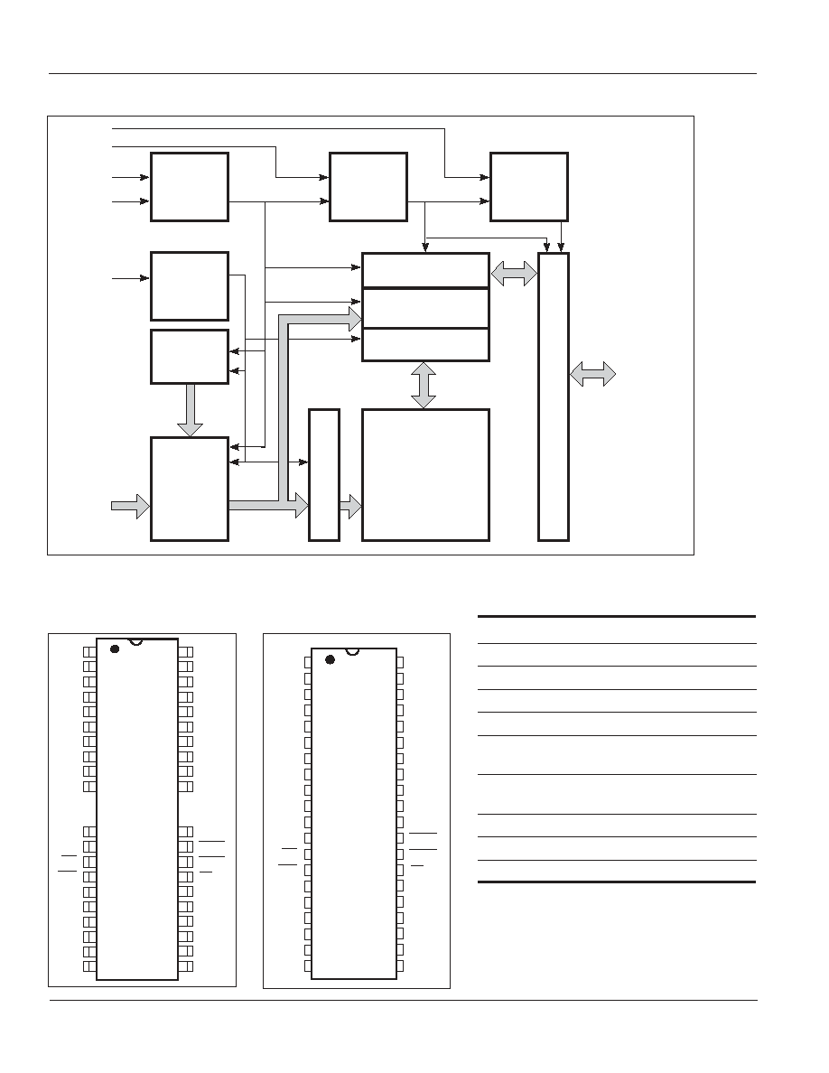
FUNCTIONAL DESCRIPTION
The IS41C16257A and the IS41LV16257A are CMOS DRAMs
optimized for high-speed bandwidth, low-power applications.
During READ or WRITE cycles, each bit is uniquely
addressed through the 18 address bits. These are entered
nine bits (A0-A8) at a time. The row address is latched by
the Row Address Strobe (
RAS
). The column address is
latched by the Column Address Strobe (
CAS
).
RAS
is used
to latch the first nine bits and
CAS
is used to latch the latter
nine bits.
The IS41C16257A and the IS41LV16257A has two
CAS
controls,
LCAS
and
UCAS
. The
LCAS
and
UCAS
inputs
internally generate a
CAS
signal functioning in an identical
manner to the single
CAS
input on the other 256K x 16
DRAMs. The key difference is that each
CAS
controls its
corresponding I/O tristate logic (in conjunction with
OE
and
WE
and
RAS
).
LCAS
controls I/O0 - I/O7 and
UCAS
controls I/O8 - I/O15.
The IS41C16257A and the IS41LV16257A
CAS
function is
determined by the first
CAS
(
LCAS
or
UCAS
) transitioning
LOW and the last transitioning back HIGH. The two
CAS
controls give the IS41C16257A both BYTE READ and BYTE
WRITE cycle capabilities.
Memory Cycle
A memory cycle is initiated by bringing
RAS
LOW and it is
terminated by returning both
RAS
and
CAS
HIGH. To
ensure proper device operation and data integrity any
memory cycle, once initiated, must not be ended or aborted
before the minimum t
RAS
time has expired. A new cycle
must not be initiated until the minimum precharge time t
RP
,
t
CP
has elapsed.
Read Cycle
A read cycle is initiated by the falling edge of
CAS
or
OE
,
whichever occurs last, while holding
WE
HIGH. The column
address must be held for a minimum time specified by t
AR
.
Data Out becomes valid only when t
RAC
, t
AA
, t
CAC
and t
OEA
are all satisfied. As a result, the access time is dependent
on the timing relationships between these parameters.
Write Cycle
A write cycle is initiated by the falling edge of
CAS
and
WE
,
whichever occurs last. The input data must be valid at or
before the falling edge of
CAS
or
WE
, whichever occurs last.
Refresh Cycle
To retain data, 512 refresh cycles are required in each
8 ms period. There are two ways to refresh the memory:
1. By clocking each of the 512 row addresses (A0 through
A8) with
RAS
at least once every 8 ms. Any read, write,
read-modify-write or
RAS
-only cycle refreshes the ad-
dressed row.
2. Using a
CAS
-before-
RAS
refresh cycle.
CAS
-before-
RAS
refresh is activated by the falling edge of
RAS
, while
holding
CAS
LOW. In
CAS
-before-
RAS
refresh cycle, an
internal 9-bit counter provides the row addresses and the
external address inputs are ignored.
CAS
-before-
RAS
is a refresh-only mode and no data access
or device selection is allowed. Thus, the output remains in
the High-Z state during the cycle.
Power-On
After application of the V
CC
supply, an initial pause of
200 µs is required followed by a minimum of eight initialization
cycles (any combination of cycles containing a
RAS
signal).
During power-on, it is recommended that
RAS
track with V
CC
or be held at a valid V
IH
to avoid current surges.
IS41C16257A
IS41LV16257A
ISSI
Æ
Integrated Silicon Solution, Inc. -- 1-800-379-4774
5
Rev. B
04/22/05
ABSOLUTE MAXIMUM RATINGS
(1)
Symbol
Parameters
Rating
Unit
V
T
Voltage on Any Pin Relative to GND
5V
≠1.0 to +7.0
V
3.3V
≠0.5 t0 +4.6
V
CC
Supply Voltage
5V
≠1.0 to +7.0
V
3.3V
≠0.5 t0 +4.6
I
OUT
Output Current
50
mA
P
D
Power Dissipation
1
W
T
A
Operation Temperature
Com.
0 to +70
∞C
T
STG
Storage Temperature
≠55 to +125
∞C
Note:
1. Stress greater than those listed under ABSOLUTE MAXIMUM RATINGS may cause
permanent damage to the device. This is a stress rating only and functional operation of the
device at these or any other conditions above those indicated in the operational sections of
this specification is not implied. Exposure to absolute maximum rating conditions for
extended periods may affect reliability.
RECOMMENDED OPERATING CONDITIONS
(Voltages are referenced to GND)
Symbol
Parameter
Voltage
Min.
Typ.
Max.
Unit
V
CC
Supply Voltage
5V
4.5
5.0
5.5
V
V
CC
Supply Voltage
3.3V
3.0
3.3
3.6
V
V
IH
Input High Voltage
5V
2.4
--
V
CC
+ 1.0
V
V
IH
Input High Voltage
3.3V
2.0
--
V
CC
+ 0.3
V
V
IL
Input Low Voltage
5V
≠1.0
--
0.8
V
V
IL
Input Low Voltage
3.3
≠0.3
--
0.8
V
T
A
Ambient Temperature
Com.
0
--
70
∞C
CAPACITANCE
(1,2)
Symbol
Parameter
Max.
Unit
C
IN
1
Input Capacitance: A0-A8
5
pF
C
IN
2
Input Capacitance:
RAS
,
UCAS
,
LCAS
,
WE
,
OE
7
pF
C
IO
Data Input/Output Capacitance: I/O0-I/O15
7
pF
Notes:
1. Tested initially and after any design or process changes that may affect these parameters.
2. Test conditions: T
A
= 25∞C, f = 1 MHz, V
CC
= 5.0V + 10% or Vcc=3.3V ± 10%.