
IS42VS16100D
ISSI
Æ
Integrated Silicon Solution, Inc. -- www.issi.com --
1-800-379-4774
1
Rev. 00D
06/30/05
Copyright © 2005 Integrated Silicon Solution, Inc. All rights reserved. ISSI reserves the right to make changes to this specification and its products at any time
without notice. ISSI assumes no liability arising out of the application or use of any information, products or services described herein. Customers are advised to
obtain the latest version of this device specification before relying on any published information and before placing orders for products.
ADVANCED INFORMATION
JULY 2005
FEATURES
∑ Clock frequency: 135, 100, 83 MHz
∑
Power Supply: 1.8V
∑
Fully synchronous; all signals referenced to a
positive clock edge
∑
Two banks can be operated simultaneously and
independently
∑
Dual internal bank controlled by A11 (bank
select)
∑
Programmable burst length (1, 2, 4, 8, full page)
∑
Programmable burst sequence: Sequential/
Interleave
∑
Programmable full and half drive strength
∑
Programmable
CAS
latency (2, 3 clocks)
∑
2048 refresh cycles every 32 ms
∑
Random column address every clock cycle
∑
Burst read/write and burst read/single write
operations capability
∑
Byte controlled by LDQM and UDQM
∑
Auto Refresh and Self Refresh modes
∑
Partial Array Self-Refresh
∑
Power Down and Deep Power Down
∑
Lead-free package options
DESCRIPTION
ISSI
's 16Mb Synchronous DRAM IS42VS16100D is
organized as a 524,288-word x 16-bit x 2-bank for
improved performance. The synchronous DRAMs
achieve high-speed data transfer using pipeline
architecture. All inputs and outputs signals refer to the
rising edge of the clock input.
512K Words x 16 Bits x 2 Banks (16-MBIT)
SYNCHRONOUS DYNAMIC RAM
KEY TIMING PARAMETERS
Parameter
-7.5
-10
Unit
Clock Cycle Time
CAS
Latency = 3
7.4
10
ns
CAS
Latency = 2
10
12
ns
Clock Frequency
CAS
Latency = 3
133
100
MHz
CAS
Latency = 2
100
83
MHz
Access Time from Clock
CAS
Latency = 3
6
7
ns
CAS
Latency = 2
8
8
ns
IS42VS16100D
ISSI
Æ
2
Integrated Silicon Solution, Inc. -- www.issi.com --
1-800-379-4774
Rev. 00D
06/30/05
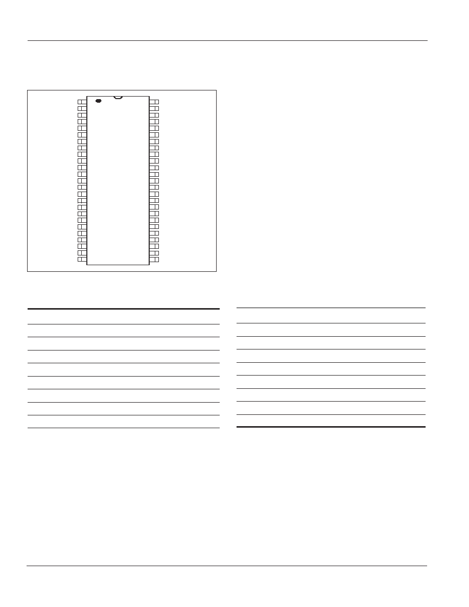
PIN CONFIGURATIONS
50-Pin TSOP (Type II)
PIN DESCRIPTIONS
A0-A11
Address Input
A0-A10
Row Address Input
A11
Bank Select Address
A0-A7
Column Address Input
DQ0 to DQ15
Data DQ
CLK
System Clock Input
CKE
Clock Enable
CS
Chip Select
RAS
Row Address Strobe Command
CAS
Column Address Strobe Command
WE
Write Enable
LDQM
Lower Bye, Input/Output Mask
UDQM
Upper Bye, Input/Output Mask
VDD
Power
GND
Ground
VDDQ
Power Supply for DQ Pin
GNDQ
Ground for DQ Pin
NC
No Connection
1
2
3
4
5
6
7
8
9
10
11
12
13
14
15
16
17
18
19
20
21
22
23
24
25
50
49
48
47
46
45
44
43
42
41
40
39
38
37
36
35
34
33
32
31
30
29
28
27
26
VDD
DQ0
DQ1
GNDQ
DQ2
DQ3
VDDQ
DQ4
DQ5
GNDQ
DQ6
DQ7
VDDQ
LDQM
WE
CAS
RAS
CS
A11
A10
A0
A1
A2
A3
VDD
GND
DQ15
IDQ14
GNDQ
DQ13
DQ12
VDDQ
DQ11
DQ10
GNDQ
DQ9
DQ8
VDDQ
NC
UDQM
CLK
CKE
NC
A9
A8
A7
A6
A5
A4
GND

IS42VS16100D
ISSI
Æ
Integrated Silicon Solution, Inc. -- www.issi.com --
1-800-379-4774
3
Rev. 00D
06/30/05
PIN FUNCTIONS
Pin No.
Symbol
Type
Function (In Detail)
20 to 24
A0-A10
Input Pin
A0 to A10 are address inputs. A0-A10 are used as row address inputs during active
27 to 32
command input and A0-A7 as column address inputs during read or write command
input. A10 is also used to determine the precharge mode during other commands. If
A10 is LOW during precharge command, the bank selected by A11 is precharged,
but if A10 is HIGH, both banks will be precharged.
When A10 is HIGH in read or write command cycle, the precharge starts
automatically after the burst access.
These signals become part of the OP CODE during mode register set command
input.
19
A11
Input Pin
A11 is the bank selection signal. When A11 is LOW, bank 0 is selected and when
high, bank 1 is selected. This signal becomes part of the OP CODE during mode
register set command input.
16
CAS
Input Pin
CAS
, in conjunction with the
RAS
and
WE
, forms the device command. See the
"Command Truth Table" item for details on device commands.
34
CKE
Input Pin
The CKE input determines whether the CLK input is enabled within the device. When
is CKE HIGH, the next rising edge of the CLK signal will be valid, and when LOW,
invalid. When CKE is LOW, the device will be in either the power-down mode, the
clock suspend mode, or the self refresh mode. The CKE is an asynchronous input.
35
CLK
Input Pin
CLK is the master clock input for this device. Except for CKE, all inputs to this device
are acquired in synchronization with the rising edge of this pin.
18
CS
Input Pin
The
CS
input determines whether command input is enabled within the device.
Command input is enabled when
CS
is LOW, and disabled with
CS
is HIGH. The
device remains in the previous state when
CS
is HIGH.
2, 3, 5, 6, 8, 9, 11
DQ0 to
DQ Pin
DQ0 to DQ15 are DQ pins. DQ through these pins can be controlled in byte units
12, 39, 40, 42, 43,
DQ15
using the LDQM and UDQM pins.
45, 46, 48, 49
14, 36
LDQM,
Input Pin
LDQM and UDQM control the lower and upper bytes of the DQ buffers. In read
UDQM
mode, LDQM and UDQM control the output buffer. When LDQM or UDQM is LOW,
the corresponding buffer byte is enabled, and when HIGH, disabled. The outputs go
to the HIGH impedance state when LDQM/UDQM is HIGH. This function
corresponds to
OE
in conventional DRAMs. In write mode, LDQM and UDQM control
the input buffer. When LDQM or UDQM is LOW, the corresponding buffer byte is
enabled, and data can be written to the device. When LDQM or UDQM is HIGH, input
data is masked and cannot be written to the device.
17
RAS
Input Pin
RAS
, in conjunction with
CAS
and
WE
, forms the device command. See the
"Command Truth Table" item for details on device commands.
15
WE
Input Pin
WE
, in conjunction with
RAS
and
CAS
, forms the device command. See the
"Command Truth Table" item for details on device commands.
7, 13, 38, 44
VDDQ
Power Supply Pin
VDDQ is the output buffer power supply.
1, 25
VDD
Power Supply Pin
VDD is the device internal power supply.
4, 10, 41, 47
GNDQ
Power Supply Pin
GNDQ is the output buffer ground.
26, 50
GND
Power Supply Pin
GND is the device internal ground.
IS42VS16100D
ISSI
Æ
4
Integrated Silicon Solution, Inc. -- www.issi.com --
1-800-379-4774
Rev. 00D
06/30/05
FUNCTIONAL BLOCK DIAGRAM
CLK
CKE
CS
RAS
CAS
WE
A11
A9
A8
A7
A6
A5
A4
A3
A2
A1
A0
A10
COMMAND
DECODER
&
CLOCK
GENERATOR
MODE
REGISTER
REFRESH
CONTROLLER
REFRESH
COUNTER
SELF
REFRESH
CONTROLLER
ROW
ADDRESS
LATCH
MUL
TIPLEXER
ROW
ADDRESS
BUFFER
ROW
ADDRESS
BUFFER
COLUMN
ADDRESS LA
TCH
B
U
RST COUNTER
COLUMN
ADDRESS B
UFFER
R
O
W DECODER
R
O
W DECODER
MEMORY CELL
ARRAY
BANK 0
COLUMN DECODER
MEMORY CELL
ARRAY
BANK 1
DATA IN
BUFFER
DATA OUT
BUFFER
SENSE AMP I/O GATE
SENSE AMP I/O GATE
2048
2048
LDQM
UDQM
DQ 0-15
VDD/VDDQ
GND/GNDQ
11
11
11
11
8
11
11
8
16
16
16
16
256
256

IS42VS16100D
ISSI
Æ
Integrated Silicon Solution, Inc. -- www.issi.com --
1-800-379-4774
5
Rev. 00D
06/30/05
ABSOLUTE MAXIMUM RATINGS
(1)
Symbol
Parameters
Rating
Unit
V
DD
MAX
Maximum Supply Voltage
≠0.5 to +2.6
V
V
DD
Q
MAX
Maximum Supply Voltage for Output Buffer
≠0.5 to +2.6
V
V
IN
Input Voltage
≠0.5 to +2.6
V
P
D
MAX
Allowable Power Dissipation
1
W
I
CS
Output Shorted Current
50
mA
T
OPR
Operating Temperature
Com
0 to +70
∞C
Ext.
-25 to +85
∞C
T
STG
Storage Temperature
≠55 to +150
∞C
DC RECOMMENDED OPERATING CONDITIONS
(2)
Commercial
(
T
A
= 0∞C to +70∞C), Extended
(
T
A
= -25∞C to +85∞C)
Symbol
Parameter
Min.
Typ.
Max.
Unit
V
DD
, V
DD
Q
Supply Voltage
1.7
1.8
1.9
V
V
IH
Input High Voltage
(3)
0.8 x V
DDQ
--
V
DDQ
+ 0.3
V
V
IL
Input Low Voltage
(4)
-0.3
--
+0.3
V
CAPACITANCE CHARACTERISTICS
(1,2)
(V
DD
= 1.8V, T
A
= +25∞C, f = 1 MHz)
Symbol
Parameter
Min.
Max.
Unit
C
IN
1
Input Capacitance: CLK
2.5
4.0
pF
C
IN
2
Input Capacitance: (A0-A11, CKE,
CS
,
RAS
,
CAS
,
WE
, LDQM, UDQM) 2.5
5.0
pF
CI/O
Data Input/Output Capacitance: DQ0-DQ15
4.0
6.5
pF
Notes:
1. Stress greater than those listed under ABSOLUTE MAXIMUM RATINGS may cause permanent damage to the device. This
is a stress rating only and functional operation of the device at these or any other conditions above those indicated in the
operational sections of this specification is not implied. Exposure to absolute maximum rating conditions for extended
periods may affect reliability.
2. All voltages are referenced to Vss.
3. V
IH
(max) = 2.2V with a pulse width
3 ns.
4. V
IL
(min) = -1.0V with a pulse width
3 ns.

IS42VS16100D
ISSI
Æ
6
Integrated Silicon Solution, Inc. -- www.issi.com --
1-800-379-4774
Rev. 00D
06/30/05
DC ELECTRICAL CHARACTERISTICS
(Recommended Operation Conditions unless otherwise noted.)
Continued on next page.
Symbol
Parameter
Test Condition
Min.
Max.
Unit
I
IL
Input Leakage Current
0V
V
IN
V
DD
, with pins other than
≠1.0
1.0
µA
the tested pin at 0V
I
OL
Output Leakage Current
Output is disabled, 0V
V
OUT
V
DD
≠1.5
1.5
µA
V
OH
Output High Voltage Level
(1)
I
OH
= ≠0.1 mA
0.9 x V
DDQ
--
V
V
OL
Output Low Voltage Level
(1)
I
OL
= 0.1 mA
--
0.2
V

IS42VS16100D
ISSI
Æ
Integrated Silicon Solution, Inc. -- www.issi.com --
1-800-379-4774
7
Rev. 00D
06/30/05
DC ELECTRICAL CHARACTERISTICS
(Recommended Operation Conditions unless otherwise noted.)
Symbol Parameter
Test Condition
Speed
Min.
Max.
Unit
I
CC1
Operating Current
(1,2)
One Bank Operation,
CAS
Latency = 3
-7.5
--
45
mA
Burst Length=1
-10
--
35
mA
t
RC
t
RC
(min.)
CAS
Latency = 2
-7.5
--
50
mA
I
OUT
= 0mA
-10
--
40
I
CC2P
Precharge Standby Current CKE
V
IL
(
MAX
)
t
CK
= 10 ns
--
--
0.3
mA
(In Power-Down Mode)
I
CC2PS
Precharge Standby Current CKE
V
IL
(
MAX
)
t
CK
=
--
--
0.3
mA
(In Power-Down Mode)
CLK
V
IL
(
MAX
)
I
CC2N
Active Standby Current
(3)
CKE
V
IH
(
MIN
)
t
CK
= 10 ns
--
--
6
mA
(In Non Power-Down Mode)
CS
V
IH
(
MIN
),
I
CC2NS
Active Standby Current
CKE
V
IH
(
MIN
)
t
CK
=
--
--
2
mA
(In Non Power-Down Mode) Inputs are stable
I
CC3P
Active Standby Current
CKE
V
IL
(
MAX
)
t
CK
= 10 ns
--
--
6
mA
(In Non Power-Down Mode)
I
CC3PS
Active Standby Current
CKE
V
IL
(
MAX
)
t
CK
=
--
--
5
mA
(In Non Power-Down Mode) CLK
V
IL
(
MAX
)
I
CC3N
Active Standby Current
(3)
CKE
V
IH
(
MIN
)
t
CK
= 10 ns
--
--
12
mA
(In Non Power-Down Mode)
CS
V
IH
(
MIN
)
I
CC3NS
Active Standby Current
CKE
V
IH
(
MIN
)
t
CK
=
--
--
10
mA
(In Non Power-Down Mode) CLK
V
IL
(
MAX
)
Inputs are stable
I
CC4
Operating Current
t
CK
= t
CK
(
MIN
)
CAS
latency = 2, 3
-7.5
--
60
mA
(In Burst Mode)
(1,3)
I
OUT
= 0mA
-10
--
50
mA
Page Burst
Both Banks activated
I
CC5
Auto-Refresh Current
t
RC
= t
RC
(
MIN
)
CAS
latency = 2, 3
-7.5
--
40
mA
-10
--
40
mA
I
CC6
Self-Refresh Current
CKE
0.2V
PASR = Full, T
A
+40
o
C
--
--
110
µ
A
PASR = 1 Bank, T
A
+40
o
C
--
--
85
µ
A
PASR = 1/2 Bank, T
A
+40
o
C
--
--
65
µ
A
PASR = 1/4 Bank, T
A
+40
o
C
--
--
60
µ
A
PASR = Full, T
A
+85
o
C
--
--
260
µ
A
PASR = 1 Bank, T
A
+85
o
C
--
--
180
µ
A
PASR = 1/2 Bank, T
A
+85
o
C
--
--
130
µ
A
PASR = 1/4 Bank, T
A
+85
o
C
--
--
95
µ
A
I
CC7
Deep Power Down Current CKE
0.2V
--
--
10
µ
A
Notes:
1. These are the values at the minimum cycle time. Since the currents are transient, these values decrease as the cycle time
increases. Also note that a bypass capacitor of at least 0.01 µF should be inserted between V
DD
and Vss for each memory
chip to suppress power supply voltage noise (voltage drops) due to these transient currents.
2. Icc
1
and Icc
4
depend on the output load. The maximum values for Icc
1
and Icc
4
are obtained with the output open state.
3. Inputs changed once every two clocks.

IS42VS16100D
ISSI
Æ
8
Integrated Silicon Solution, Inc. -- www.issi.com --
1-800-379-4774
Rev. 00D
06/30/05
AC CHARACTERISTICS
(1,2,3)
-7.5
-10
Symbol Parameter
Min.
Max.
Min.
Max.
Units
t
CK
3
Clock Cycle Time
CAS
Latency = 3
7.4
--
10
--
ns
t
CK
2
CAS
Latency = 2
10
--
12
--
ns
t
AC
3
Access Time From CLK
(4)
CAS
Latency = 3
--
6
--
7
ns
t
AC
2
CAS
Latency = 2
--
8
--
8
ns
t
CHI
CLK HIGH Level Width
2.5
--
3
--
ns
t
CL
CLK LOW Level Width
2.5
--
3
--
ns
t
OH
3
Output Data Hold Time
CAS
Latency = 3
2
--
2
--
ns
t
OH
2
CAS
Latency = 2
2
--
2
--
ns
t
LZ
Output LOW Impedance Time
0
--
0
--
ns
t
HZ
3
Output HIGH Impedance Time
(5)
CAS
Latency = 3
--
6
--
7
ns
t
HZ
2
CAS
Latency = 2
--
8
--
8
ns
t
DS
Input Data Setup Time
2
--
2
--
ns
t
DH
Input Data Hold Time
1
--
1
--
ns
t
AS
Address Setup Time
2
--
2
--
ns
t
AH
Address Hold Time
1
--
1
--
ns
t
CKS
CKE Setup Time
1.5
--
2.5
--
ns
t
CKH
CKE Hold Time
1
--
1
--
ns
t
CKA
CKE to CLK Recovery Delay Time
1CLK+3 --
1CLK+3
--
ns
t
CS
Command Setup Time (
CS
,
RAS
,
CAS
,
WE
, DQM)
1.5
--
2
--
ns
t
CH
Command Hold Time (
CS
,
RAS
,
CAS
,
WE
, DQM)
1
--
1
--
ns
t
RC
Command Period (REF to REF / ACT to ACT)
72
--
94
--
ns
t
RAS
Command Period (ACT to PRE)
45 100,000
50
100,000
ns
t
RP
Command Period (PRE to ACT)
19
--
24
--
ns
t
RCD
Active Command To Read / Write Command Delay Time
19
--
24
--
ns
t
RRD
Command Period (ACT [0] to ACT[1])
14
--
18
--
ns
t
DPL
3
Input Data To Precharge
CAS
Latency = 3
2CLK
--
2CLK
--
ns
Command Delay time
t
DPL
2
CAS
Latency = 2
2CLK
--
2CLK
--
ns
t
DAL
3
Input Data To Active / Refresh
CAS
Latency = 3
2CLK+t
RP
--
2CLK+t
RP
--
ns
Command Delay time (During Auto-Precharge)
t
DAL
2
CAS
Latency = 2
2CLK+t
RP
--
2CLK+t
RP
--
ns
t
T
Transition Time
0.5
5
0.5
5
ns
t
REF
Refresh Cycle Time (2048)
--
32
--
32
ms
Notes:
1. The power-on sequence must be executed before starting memory operation.
2. Measured with t
T
= 0.5 ns.
3. The reference level is 0.9V when measuring input signal timing. Rise and fall times are measured between V
IH
(min.) and V
IL
(max.).
4. Access time is measured at 0.9V with the load shown in the figure below.
5. The time t
HZ
(max.) is defined as the time required for the output voltage to become high impedance.
IS42VS16100D
ISSI
Æ
Integrated Silicon Solution, Inc. -- www.issi.com --
1-800-379-4774
9
Rev. 00D
06/30/05
OPERATING FREQUENCY / LATENCY RELATIONSHIPS
SYMBOL PARAMETER
-7.5
-7.5/-10
-10
UNITS
--
Clock Cycle Time
7.4
10
12
ns
--
Operating Frequency
135
100
83
MHz
t
CAC
CAS
Latency
3
2/3
2
cycle
t
RCD
Active Command To Read/Write Command Delay Time
3
3
2
cycle
t
RAC
RAS
Latency (t
RCD
+ t
CAC
)
6
6
4
cycle
t
RC
Command Period (REF to REF / ACT to ACT)
10
10
8
cycle
t
RAS
Command Period (ACT to PRE)
6
5
5
cycle
t
RP
Command Period (PRE to ACT)
3
3
2
cycle
t
RRD
Command Period (ACT[0] to ACT [1])
2
2
2
cycle
t
CCD
Column Command Delay Time
1
1
1
cycle
(READ, READA, WRIT, WRITA)
t
DPL
Input Data To Precharge Command Delay Time
2
2
2
cycle
t
DAL
Input Data To Active/Refresh Command Delay Time
5
5
4
cycle
(During Auto-Precharge)
t
RBD
Burst Stop Command To Output in HIGH-Z Delay Time
CAS
Latency = 3
3
3
--
cycle
(Read)
CAS
Latency = 2
--
2
2
t
WBD
Burst Stop Command To Input in Invalid Delay Time
0
0
0
cycle
(Write)
t
RQL
Precharge Command To Output in HIGH-Z Delay Time
CAS
Latency = 3
3
3
--
cycle
(Read)
CAS
Latency = 2
--
2
2
t
WDL
Precharge Command To Input in Invalid Delay Time
0
0
0
cycle
(Write)
t
PQL
Last Output To Auto-Precharge Start Time (Read)
CAS
Latency = 3
-2
≠2
--
cycle
CAS
Latency = 2
--
-1
-1
t
QMD
DQM To Output Delay Time (Read)
2
2
2
cycle
t
DMD
DQM To Input Delay Time (Write)
0
0
0
cycle
t
MRD
Mode Register Set To Command Delay Time
2
2
2
cycle
AC TEST CONDITIONS
(Input/Output Reference Level: 0.9V)
I/O
50
0.5 x VDDQ V
30 pF
Output Load
Input
t
OH
t
AC
0.9V
0.9V
t
CH
t
CS
t
CK
t
CHI
t
CL
1.8V
0.9V
0.0V
1.8V
0.9V
0.0V
CLK
INPUT
OUTPUT
IS42VS16100D
ISSI
Æ
10
Integrated Silicon Solution, Inc. -- www.issi.com --
1-800-379-4774
Rev. 00D
06/30/05
COMMANDS
CLK
CKE
HIGH
ROW
ROW
BANK 1
BANK 0
CS
RAS
CAS
WE
A0-A9
A10
A11
CLK
CKE
HIGH
COLUMN
BANK 1
AUTO PRECHARGE
NO PRECHARGE
BANK 0
CS
RAS
CAS
WE
A0-A9
A10
A11
(1)
CLK
CKE
HIGH
COLUMN
AUTO PRECHARGE
BANK 1
BANK 0
CS
RAS
CAS
WE
A0-A9
A10
A11
CLK
CKE
HIGH
BANK 1
BANK 0 AND BANK 1
BANK 0 OR BANK 1
NO PRECHARGE
BANK 0
CS
RAS
CAS
WE
A0-A9
A10
A11
(1)
Notes:
1. A8-A9 = Don't Care.
Don't Care
Active Command Read Command
Write Command
Precharge Command
IS42VS16100D
ISSI
Æ
Integrated Silicon Solution, Inc. -- www.issi.com --
1-800-379-4774
11
Rev. 00D
06/30/05
COMMANDS
(cont.)
CLK
CKE
HIGH
CS
RAS
CAS
WE
A0-A9
A10
A11
CLK
CKE
HIGH
CS
RAS
CAS
WE
A0-A9
A10
A11
CLK
CKE
HIGH
CS
RAS
CAS
WE
A0-A9
A10
A11
CLK
CKE
HIGH
CS
RAS
CAS
WE
A0-A9
A10
A11
OP-CODE
OP-CODE
OP-CODE
Don't Care
No-Operation Command Device Deselect Command
Mode Register Set Command
Auto-Refresh Command
IS42VS16100D
ISSI
Æ
12
Integrated Silicon Solution, Inc. -- www.issi.com --
1-800-379-4774
Rev. 00D
06/30/05
COMMANDS
(cont.)
CLK
CKE
CS
RAS
CAS
WE
A0-A9
A10
A11
CLK
CKE
CS
RAS
CAS
WE
A0-A9
A10
A11
BANK(S) ACTIVE
HIGH
NOP
NOP
NOP
NOP
CLK
CKE
CS
RAS
CAS
WE
A0-A9
A10
A11
CLK
CKE
CS
RAS
CAS
WE
A0-A9
A10
A11
ALL BANKS IDLE
Power Down
Deep Power Down
Power Down or Deep Power Down
Command
Clock Suspend Command
Burst Stop Command
Self-Refresh Command

IS42VS16100D
ISSI
Æ
Integrated Silicon Solution, Inc. -- www.issi.com --
1-800-379-4774
13
Rev. 00D
06/30/05
Mode Register Set Command
(
CS
,
RAS
,
CAS
,
WE
= LOW)
The IS42VS16100D product incorporates a register that
defines the device operating mode. This command
functions as a data input pin that loads this register from
the pins A0 to A11. When power is first applied, the
stipulated power-on sequence should be executed and
then the IS42VS16100D should be initialized by executing
a mode register set command.
Note that the mode register set command can be executed
only when both banks are in the idle state (i.e. deactivated).
Another command cannot be executed after a mode
register set command until after the passage of the period
t
MCD
, which is the period required for mode register set
command execution.
Active Command
(
CS
,
RAS
= LOW,
CAS
,
WE
= HIGH)
The IS42VS16100D includes two banks of 4096 rows
each. This command selects one of the two banks
according to the A11 pin and activates the row selected by
the pins A0 to A10.
This command corresponds to the fall of the
RAS
signal
from HIGH to LOW in conventional DRAMs.
Precharge Command
(
CS
,
RAS
,
WE
= LOW,
CAS
= HIGH)
This command starts precharging the bank selected by
pins A10 and A11. When A10 is HIGH, both banks are
precharged at the same time. When A10 is LOW, the bank
selected by A11 is precharged. After executing this
command, the next command for the selected bank(s) is
executed after passage of the period t
RP
, which is the
period required for bank precharging.
This command corresponds to the
RAS
signal from LOW
to HIGH in conventional DRAMs
Read Command
(
CS
,
CAS
= LOW,
RAS
,
WE
= HIGH)
This command selects the bank specified by the A11 pin
and starts a burst read operation at the start address
specified by pins A0 to A7. Data is output following
CAS
latency.
The selected bank must be activated before executing
this command.
When the A10 pin is HIGH, this command functions as a
read with auto-precharge command. After the burst read
completes, the bank selected by pin A11 is precharged.
When the A10 pin is LOW, the bank selected by the A11 pin
remains in the activated state after the burst read completes.
Write Command
(
CS
,
CAS
,
WE
= LOW,
RAS
= HIGH)
When burst write mode has been selected with the mode
register set command, this command selects the bank
specified by the A11 pin and starts a burst write operation
at the start address specified by pins A0 to A7. This first
data must be input to the DQ pins in the cycle in which this
command.
The selected bank must be activated before executing this
command.
When A10 pin is HIGH, this command functions as a write
with auto-precharge command. After the burst write
completes, the bank selected by pin A11 is precharged.
When the A10 pin is low, the bank selected by the A11 pin
remains in the activated state after the burst write completes.
After the input of the last burst write data, the application
must wait for the write recovery period (t
DPL
, t
DAL
) to elapse
according to
CAS
latency.
Auto-Refresh Command
(
CS
,
RAS
,
CAS
= LOW,
WE
, CKE = HIGH)
This command executes the auto-refresh operation. The
row address and bank to be refreshed are automatically
generated during this operation.
Both banks must be placed in the idle state before executing
this command.
The stipulated period (t
RC
) is required for a single refresh
operation, and no other commands can be executed during
this period.
The device goes to the idle state after the internal refresh
operation completes.
This command must be executed at least 2048 times every
32 ms.
This command corresponds to CBR auto-refresh in
conventional DRAMs.

IS42VS16100D
ISSI
Æ
14
Integrated Silicon Solution, Inc. -- www.issi.com --
1-800-379-4774
Rev. 00D
06/30/05
Self-Refresh Command
(
CS
,
RAS
,
CAS
, CKE = LOW,
WE
= HIGH)
This command executes the self-refresh operation. The
row address to be refreshed, the bank, and the refresh
interval are generated automatically internally during this
operation. The self-refresh operation is started by dropping
the CKE pin from HIGH to LOW. The self-refresh operation
continues as long as the CKE pin remains LOW and there
is no need for external control of any other pins. The
self-refresh operation is terminated by raising the CKE pin
from LOW to HIGH. The next command cannot be executed
until the device internal recovery period (t
RC
) has elapsed.
After the self-refresh, since it is impossible to determine
the address of the last row to be refreshed, an auto-refresh
should immediately be performed for all addresses (2048
cycles).
Both banks must be placed in the idle state before
executing this command.
Burst Stop Command
(
CS
,
WE
, = LOW,
RAS
,
CAS
= HIGH)
The command forcibly terminates burst read and write
operations. When this command is executed during a
burst read operation, data output stops after the
CAS
latency period has elapsed.
No Operation
(
CS
, = LOW,
RAS
,
CAS
,
WE
= HIGH)
This command has no effect on the device.
Device Deselect Command
(
CS
= HIGH)
This command does not select the device for an object of
operation. In other words, it performs no operation with
respect to the device.
Deep Power-Down Command
(CKE = LOW)
Both banks must be idle (inactive) state prior to entering
Deep Power Down. Power consumption is reduced to the
absolute minimum. However, all data is lost in this mode.
To exit Deep Power Down, CKE must go high, and the
Power On and Initialization procedure must be followed.
Power-Down Command
(CKE = LOW,
CS
= HIGH)
When both banks are in the idle (inactive) state, or when
at least one of the banks is not in the idle (inactive) state,
this command can be used to suppress device power
dissipation by reducing device internal operations to the
minimal level in order to retain data content. Power-down
mode is started by dropping the CKE pin from HIGH to
LOW, while satisfying the other command input conditions
(see CKE Truth Table). Power-down mode continues as
long as the CKE pin is held low. All pins other than the CKE
pin are invalid and none of the other commands can be
executed in this mode. The power-down operation is
terminated by raising the CKE pin from LOW to HIGH. The
next command cannot be executed until the recovery
period (t
CKA
) has elapsed.
Since this command differs from the self-refresh command
described above in that the refresh operation is not
performed automatically internally, the refresh operation
must be performed within the refresh period (t
REF
). Thus
the maximum time that power-down mode can be held is
just under the refresh cycle time.
Clock Suspend
(CKE = LOW)
This command can be used to stop the device internal
clock temporarily during a read or write cycle. Clock
suspend mode is started by dropping the CKE pin from
HIGH to LOW. Clock suspend mode continues as long as
the CKE pin is held LOW. All input pins other than the CKE
pin are invalid and none of the other commands can be
executed in this mode. Also note that the device internal
state is maintained. Clock suspend mode is terminated by
raising the CKE pin from LOW to HIGH, at which point
device operation restarts. The next command cannot be
executed until the recovery period (t
CKA
) has elapsed.
Since this command differs from the self-refresh command
described above in that the refresh operation is not
performed automatically internally, the refresh operation
must be performed within the refresh period (t
REF
). Thus
the maximum time that clock suspend mode can be held
is just under the refresh cycle time.

IS42VS16100D
ISSI
Æ
Integrated Silicon Solution, Inc. -- www.issi.com --
1-800-379-4774
15
Rev. 00D
06/30/05
COMMAND TRUTH TABLE
(1,2)
CKE
Symbol
Command
n-1 n
CS
CS
CS
CS
CS
RAS
RAS
RAS
RAS
RAS CAS
CAS
CAS
CAS
CAS WE
WE
WE
WE
WE
DQM A11
A10
A9-A0
I/On
(E)MRS
(Extended) Mode Register Set
(3,4)
H
X
L
L
L
L
X
OP CODE
X
REF
Auto-Refresh
(5)
H
H
L
L
L
H
X
X
X
X
HIGH-Z
SREF
Self-Refresh
(5,6)
H
L
L
L
L
H
X
X
X
X
HIGH-Z
PRE
Precharge Selected Bank
H
X
L
L
H
L
X
BS
L
X
X
PALL
Precharge Both Banks
H
X
L
L
H
L
X
X
H
X
X
ACT
Bank Activate
(7)
H
X
L
L
H
H
X
BS
Row
Row
X
WRIT
Write
H
X
L
H
L
L
X
BS
L
Column
(18)
X
WRITA
Write With Auto-Precharge
(8)
H
X
L
H
L
L
X
BS
H
Column
(18)
X
READ
Read
(8)
H
X
L
H
L
H
X
BS
L
Column
(18)
X
READA
Read With Auto-Precharge
(8)
H
X
L
H
L
H
X
BS
H
Column
(18)
X
BST
Burst Stop
(9)
H
X
L
H
H
L
X
X
X
X
X
NOP
No Operation
H
X
L
H
H
H
X
X
X
X
X
DESL
Device Deselect
H
X
H
X
X
X
X
X
X
X
X
SBY
Clock Suspend / Standby Mode
L
X
X
X
X
X
X
X
X
X
X
ENB
Data Write / Output Enable
H
X
X
X
X
X
L
X
X
X
Active
MASK
Data Mask / Output Disable
H
X
X
X
X
X
H
X
X
X
HIGH-Z
DQM TRUTH TABLE
(1,2)
CKE
DQM
Symbol
Command
n-1
n
UPPER
LOWER
ENB
Data Write / Output Enable
H
X
L
L
MASK
Data Mask / Output Disable
H
X
H
H
ENBU
Upper Byte Data Write / Output Enable
H
X
L
X
ENBL
Lower Byte Data Write / Output Enable
H
X
X
L
MASKU
Upper Byte Data Mask / Output Disable
H
X
H
X
MASKL
Lower Byte Data Mask / Output Disable
H
X
X
H
CKE TRUTH TABLE
(1,2)
CKE
Symbol Command
Current State
n-1
n
CS
CS
CS
CS
CS RAS
RAS
RAS
RAS
RAS CAS
CAS
CAS
CAS
CAS WE
WE
WE
WE
WE
A11 A10 A9-A0
SPND
Start Clock Suspend Mode
Active
H
L
X
X
X
X
X
X
X
--
Clock Suspend
Other States
L
L
X
X
X
X
X
X
X
--
Terminate Clock Suspend Mode
Clock Suspend
L
H
X
X
X
X
X
X
X
REF
Auto-Refresh
Idle
H
H
L
L
L
H
X
X
X
SELF
Start Self-Refresh Mode
Idle
H
L
L
L
L
H
X
X
X
SELFX
Terminate Self-Refresh Mode
Self-Refresh
L
H
L
H
H
H
X
X
X
L
H
H
X
X
X
X
X
X
PDWN
Start Power-Down Mode
Idle
H
L
L
H
H
H
X
X
X
H
L
H
X
X
X
X
X
X
--
Terminate Power-Down Mode
Power-Down
L
H
H
X
X
X
X
X
X
L
H
L
H
H
H
X
X
X
DPD
Start Deep Power-Down Mode
Idle
H
L
L
H
H
L
X
X
X
--
Terminate Deep Power-Down Mode
Power-Down
L
H
X
X
X
X
X
X
X

IS42VS16100D
ISSI
Æ
16
Integrated Silicon Solution, Inc. -- www.issi.com --
1-800-379-4774
Rev. 00D
06/30/05
OPERATION COMMAND TABLE
(1,2)
Current State Command
Operation
CS
CS
CS
CS
CS RAS
RAS
RAS
RAS
RAS CAS
CAS
CAS
CAS
CAS WE
WE
WE
WE
WE
A11 A10 A9-A0
Idle
DESL
No Operation or Power-Down
(12)
H
X
X
X
X
X
X
NOP
No Operation or Power-Down
(12)
L
H
H
H
X
X
X
BST
Illegal
L
H
H
L
X
X
X
READ / READA
Illegal
L
H
L
H
V
V
V
(18)
WRIT/WRITA
Illegal
L
H
L
L
V
V
V
(18)
ACT
Row Active
L
L
H
H
V
V
V
(18)
PRE/PALL
No Operation
L
L
H
L
V
V
X
REF/SELF
Auto-Refresh or Self-Refresh
(13)
L
L
L
H
X
X
X
MRS
Mode Register Set
L
L
L
L
OP CODE
Row Active
DESL
No Operation
H
X
X
X
X
X
X
NOP
No Operation
L
H
H
H
X
X
X
BST
Illegal
L
H
H
L
X
X
X
READ/READA
Read Start
(17)
L
H
L
H
V
V
V
(18)
WRIT/WRITA
Write Start
(17)
L
H
L
L
V
V
V
(18)
ACT
Illegal on same bank
(10,14)
L
L
H
H
V
V
V
(18)
PRE/PALL
Precharge
(15)
L
L
H
L
V
V
X
REF/SELF
Illegal
L
L
L
H
X
X
X
MRS
Illegal
L
L
L
L
OP CODE
Read
DESL
Burst Read Continues, Row Active When Done
H
X
X
X
X
X
X
NOP
Burst Read Continues, Row Active When Done
L
H
H
H
X
X
X
BST
Burst Interrupted, Row Active After Interrupt
L
H
H
L
X
X
X
READ/READA
Burst Interrupted, Read Restart After Interrupt
(16)
L
H
L
H
V
V
V
(18)
WRIT/WRITA
Burst Interrupted Write Start After Interrupt
(11,16)
L
H
L
L
V
V
V
(18)
ACT
Illegal on same bank
(10,14)
L
L
H
H
V
V
V
(18)
PRE/PALL
Burst Read Interrupted, Precharge After Interrupt
L
L
H
L
V
V
X
REF/SELF
Illegal
L
L
L
H
X
X
X
MRS
Illegal
L
L
L
L
OP CODE
Write
DESL
Burst Write Continues, Write Recovery When Done
H
X
X
X
X
X
X
NOP
Burst Write Continues, Write Recovery When Done
L
H
H
H
X
X
X
BST
Burst Write Interrupted, Row Active After Interrupt
L
H
H
L
X
X
X
READ/READA
Burst Write Interrupted, Read Start After Interrupt
(11,16)
L
H
L
H
V
V
V
(18)
WRIT/WRITA
Burst Write Interrupted, Write Restart After Interrupt
(16)
L
H
L
L
V
V
V
(18)
ACT
Illegal on same bank
(10)
L
L
H
H
V
V
V
(18)
PRE/PALL
Burst Write Interrupted, Precharge After Interrupt
L
L
H
L
V
V
X
REF/SELF
Illegal
L
L
L
H
X
X
X
MRS
Illegal
L
L
L
L
OP CODE
Read With
DESL
Burst Read Continues, Precharge When Done
H
X
X
X
X
X
X
Auto-
NOP
Burst Read Continues, Precharge When Done
L
H
H
H
X
X
X
Precharge
BST
Illegal
L
H
H
L
X
X
X
READ/READA
Illegal
L
H
L
H
V
V
V
(18)
WRIT/WRITA
Illegal
L
H
L
L
V
V
V
(18)
ACT
Illegal on same bank
(10,14)
L
L
H
H
V
V
V
(18)
PRE/PALL
Illegal
(10)
L
L
H
L
V
V
X
REF/SELF
Illegal
L
L
L
H
X
X
X
MRS
Illegal
L
L
L
L
OP CODE

IS42VS16100D
ISSI
Æ
Integrated Silicon Solution, Inc. -- www.issi.com --
1-800-379-4774
17
Rev. 00D
06/30/05
OPERATION COMMAND TABLE
(1,2)
Current State Command
Operation
CS
CS
CS
CS
CS RAS
RAS
RAS
RAS
RAS CAS
CAS
CAS
CAS
CAS WE
WE
WE
WE
WE
A11 A10 A9-A0
Write With
DESL
Burst Write Continues, Write Recovery And Precharge
H
X
X
X
X
X
X
Auto-Precharge
NOP
Burst Write Continues, Write Recovery And Precharge
L
H
H
H
X
X
X
BST
Illegal
L
H
H
L
X
X
X
READ/READA
Illegal
(10)
L
H
L
H
V
V
V(18)
WRIT/WRITA
Illegal
(10)
L
H
L
L
V
V
V(18)
ACT
Illegal on the same bank
(10)
L
L
H
H
V
V
V(18)
PRE/PALL
Illegal
(10)
L
L
H
L
V
V
X
REF/SELF
Illegal
L
L
L
H
X
X
X
MRS
Illegal
L
L
L
L
OPCODE
Row Precharge
DESL
No Operation, Idle State After t
RP
Has Elapsed
H
X
X
X
X
X
X
NOP
No Operation, Idle State After t
RP
Has Elapsed
L
H
H
H
X
X
X
BST
Illegal
L
H
H
L
X
X
X
READ/READA
Illegal
(10)
L
H
L
H
V
V
V(18)
WRIT/WRITA
Illegal
(10)
L
H
L
L
V
V
V(18)
ACT
Illegal
(10)
L
L
H
H
V
V
V(18)
PRE/PALL
No Operation on same bank;
L
L
H
L
V
V
X
Idle State After t
RP
Has Elapsed
(10)
REF/SELF
Illegal
L
L
L
H
X
X
X
MRS
Illegal
L
L
L
L
OP CODE
Immediately
DESL
No Operation, Row Active After t
RCD
Has Elapsed
H
X
X
X
X
X
X
Following
NOP
No Operation, Row Active After t
RCD
Has Elapsed
L
H
H
H
X
X
X
Row Active
BST
Illegal
L
H
H
L
X
X
X
READ/READA
Illegal
(10)
L
H
L
H
V
V
V(18)
WRIT/WRITA
Illegal
(10)
L
H
L
L
V
V V(18)
ACT
Illegal on same bank
(10,14)
L
L
H
H
V
V V(18)
PRE/PALL
Illegal
(10,15)
L
L
H
L
V
V
X
REF/SELF
Illegal
L
L
L
H
X
X
X
MRS
Illegal
L
L
L
L
OP CODE

IS42VS16100D
ISSI
Æ
18
Integrated Silicon Solution, Inc. -- www.issi.com --
1-800-379-4774
Rev. 00D
06/30/05
OPERATION COMMAND TABLE
(1,2)
Current State Command
Operation
CS
CS
CS
CS
CS RAS
RAS
RAS
RAS
RAS CAS
CAS
CAS
CAS
CAS WE
WE
WE
WE
WE
A11 A10 A9-A0
Auto-Refresh
DESL
No Operation, Idle State After t
RP
Has Elapsed
H
X
X
X
X
X
X
NOP
No Operation, Idle State After t
RP
Has Elapsed
L
H
H
H
X
X
X
BST
Illegal
L
H
H
L
X
X
X
READ/READA
Illegal
L
H
L
H
V
V
V
(18)
WRIT/WRITA
Illegal
L
H
L
L
V
V
V
(18)
ACT
Illegal
L
L
H
H
V
V
V
(18)
PRE/PALL
Illegal
L
L
H
L
V
V
X
REF/SELF
Illegal
L
L
L
H
X
X
X
MRS
Illegal
L
L
L
L
OP CODE
Mode Register DESL
No Operation, Idle State After t
MCD
Has Elapsed
H
X
X
X
X
X
X
Set
NOP
No Operation, Idle State After t
MCD
Has Elapsed
L
H
H
H
X
X
X
BST
Illegal
L
H
H
L
X
X
X
READ/READA
Illegal
L
H
L
H
V
V
V
(18)
WRIT/WRITA
Illegal
L
H
L
L
V
V
V
(18)
ACT
Bank and Row Active
(19)
L
L
H
H
V
V
V
(18)
PRE/PALL
No Operation
L
L
H
L
V
V
X
REF/SELF
Refresh
(19)
L
L
L
H
X
X
X
MRS
Mode Register Set
(19)
L
L
L
L
OP CODE
Notes:
1. H: HIGH level input, L: LOW level input, X: HIGH or LOW level input, V: Valid data input, BS: Bank Select (High or Low).
2. All input signals are latched on the rising edge of the CLK signal.
3. Both banks must be placed in the inactive (idle) state in advance.
4. The state of the A0 to A11 pins is loaded into the mode register as an OP code.
5. The row address is generated automatically internally at this time. The DQ pin and the address pin data is ignored.
6. During a self-refresh operation, all pin data (states) other than CKE is ignored.
7. The selected bank must be placed in the inactive (idle) state in advance.
8. The selected bank must be placed in the active state in advance.
9. This command is valid only when the burst length set to full page.
10. This is possible depending on the state of the bank selected by the A11 pin.
11. Time to switch internal buses is required.
12. The IS42VS16100D can be switched to power-down mode by dropping the CKE pin LOW when both banks in the idle
state. Input pins other than CKE are ignored at this time.
13. The IS42VS16100D can be switched to self-refresh mode by dropping the CKE pin LOW when both banks in the idle state.
Input pins other than CKE are ignored at this time.
14. Possible if t
RRD
is satisfied.
15. Illegal if t
RAS
is not satisfied.
16. The conditions for burst interruption must be observed. Also note that the IS42VS16100D will enter the precharged state
immediately after the burst operation completes if auto-precharge is selected.
17. Command input becomes possible after the period t
RCD
has elapsed. Also note that the IS42VS16100D will enter the
precharged state immediately after the burst operation completes if auto-precharge is selected.
18. A8,A9 = don't care.
19. Illegal if t
MRD
is not satisfied.

IS42VS16100D
ISSI
Æ
Integrated Silicon Solution, Inc. -- www.issi.com --
1-800-379-4774
19
Rev. 00D
06/30/05
CKE RELATED COMMAND TRUTH TABLE
(1)
CKE
Current State
Operation
n-1
n
CS
CS
CS
CS
CS RAS
RAS
RAS
RAS
RAS CAS
CAS
CAS
CAS
CAS WE
WE
WE
WE
WE
A11 A10 A9-A0
Self-Refresh
Undefined
H
X
X
X
X
X
X
X
X
Self-Refresh Recovery
(2)
L
H
H
X
X
X
X
X
X
Self-Refresh Recovery
(2)
L
H
L
H
H
X
X
X
X
Illegal
(2)
L
H
L
H
L
X
X
X
X
Illegal
(2)
L
H
L
L
X
X
X
X
X
Self-Refresh
L
L
X
X
X
X
X
X
X
Self-Refresh Recovery
Idle State After t
RC
Has Elapsed
H
H
H
X
X
X
X
X
X
Idle State After t
RC
Has Elapsed
H
H
L
H
H
X
X
X
X
Illegal
H
H
L
H
L
X
X
X
X
Illegal
H
H
L
L
X
X
X
X
X
Power-Down on the Next Cycle
H
L
H
X
X
X
X
X
X
Power-Down on the Next Cycle
H
L
L
H
H
X
X
X
X
Illegal
H
L
L
H
L
X
X
X
X
Illegal
H
L
L
L
X
X
X
X
X
Power-Down
Undefined
H
X
X
X
X
X
X
X
X
Power-Down Mode Termination, Deselect Afterward
(2)
L
H
H
X
X
X
X
X
X
Power-Down Mode Termination, NOP Afterward
(2)
L
H
L
H
H
H
X
X
X
Maintain Power-Down Mode
L
L
X
X
X
X
X
X
X
Both Banks Idle
No Operation
H
H
H
X
X
X
X
X
X
See the Operation Command Table
H
H
L
H
X
X
X
X
X
Bank Active Or Precharge
H
H
L
L
H
X
X
X
X
Auto-Refresh
H
H
L
L
L
H
X
X
X
Mode Register Set
H
H
L
L
L
L
OP CODE
Enter Power Down Next Cycle
H
L
H
X
X
X
X
X
X
See the Operation Command Table
H
L
L
H
X
X
X
X
X
See the Operation Command Table
H
L
L
L
H
X
X
X
X
Self-Refresh
(3)
H
L
L
L
L
H
X
X
X
See the Operation Command Table
H
L
L
L
L
L
OP CODE
Other States
See the Operation Command Table
H
H
X
X
X
X
X
X
X
Clock Suspend on the Next Cycle
(4)
H
L
X
X
X
X
X
X
X
Clock Suspend Termination on the Next Cycle
L
H
X
X
X
X
X
X
X
Maintain Clock Suspend
L
L
X
X
X
X
X
X
X
Notes:
1. H: HIGH level input, L: LOW level input, X: HIGH or LOW level input
2. The CLK pin and the other input are reactivated asynchronously by the transition of the CKE level from LOW to HIGH. The
minimum setup time (t
CKA
) required before all commands other than mode termination must be satisfied.
3. Both banks must be set to the inactive (idle) state in advance to switch to power-down mode or self-refresh mode. Entering
Clock Suspend requires that the current state be Row Active, Read, Read with Precharge, Write, or Write with Precharge.
4. The input must be command defined in the operation command table.

IS42VS16100D
ISSI
Æ
20
Integrated Silicon Solution, Inc. -- www.issi.com --
1-800-379-4774
Rev. 00D
06/30/05
TWO BANKS OPERATION COMMAND TRUTH TABLE
(1,2)
Previous State Next State
Operation
CS
CS
CS
CS
CS RAS
RAS
RAS
RAS
RAS CAS
CAS
CAS
CAS
CAS WE
WE
WE
WE
WE
A11 A10 A9-A0
BANK 0BANK 1
BANK 0BANK 1
DESL
H
X
X
X
X
X
X
Any
Any
Any
Any
NOP
L
H
H
H
X
X
X
Any
Any
Any
Any
BST
L
H
H
L
X
X
X
R/W/A
I/A
A
I/A
I
I/A
I
I/A
I/A
R/W/A
I/A
A
I/A
I
I/A
I
READ/READA
L
H
L
H
H
H CA
(3)
I/A
R/W/A
I/A
RP
H
H CA
(3)
R/W
A
A
RP
H
L
CA
(3)
I/A
R/W/A
I/A
R
H
L
CA
(3)
R/W
A
A
R
L
H CA
(3)
R/W/A
I/A
RP
I/A
L
H CA
(3)
A
R/W
RP
A
L
L
CA
(3)
R/W/A
I/A
R
I/A
L
L
CA
(3)
A
R/W
R
A
WRIT/WRITA
L
H
L
L
H
H CA
(3)
I/A
R/W/A
I/A
WP
H
H CA
(3)
R/W
A
A
WP
H
L
CA
(3)
I/A
R/W/A
I/A
W
H
L
CA
(3)
R/W
A
A
W
L
H CA
(3)
R/W/A
I/A
WP
I/A
L
H CA
(3)
A
R/W
WP
A
L
L
CA
(3)
R/W/A
I/A
W
I/A
L
L
CA
(3)
A
R/W
W
A
ACT
L
L
H
H
H
RA
RA
Any
I
Any
A
L
RA
RA
I
Any
A
Any
PRE/PALL
L
L
H
L
X
H
X
R/W/A/I
I/A
I
I
X
H
X
I/A
R/W/A/I
I
I
H
L
X
I/A
R/W/A/I
I/A
I
H
L
X
R/W/A/I
I/A
R/W/A/I
I
L
L
X
R/W/A/I
I/A
I
I/A
L
L
X
I/A
R/W/A/I
I
R/W/A/I
REF
L
L
L
H
X
X
X
I
I
I
I
MRS
L
L
L
L
OPCODE
I
I
I
I
Notes:
1. H: HIGH level input, L: LOW level input, X: HIGH or LOW level input, RA: Row Address, CA: Column Address
2. The device state symbols are interpreted as follows:
I
Idle (inactive state)
A
Row Active State
R
Read
W
Write
RP
Read With Auto-Precharge
WP
Write With Auto-Precharge
Any Any State
3. CA: A8,A9 = don't care.
IS42VS16100D
ISSI
Æ
Integrated Silicon Solution, Inc. -- www.issi.com --
1-800-379-4774
21
Rev. 00D
06/30/05
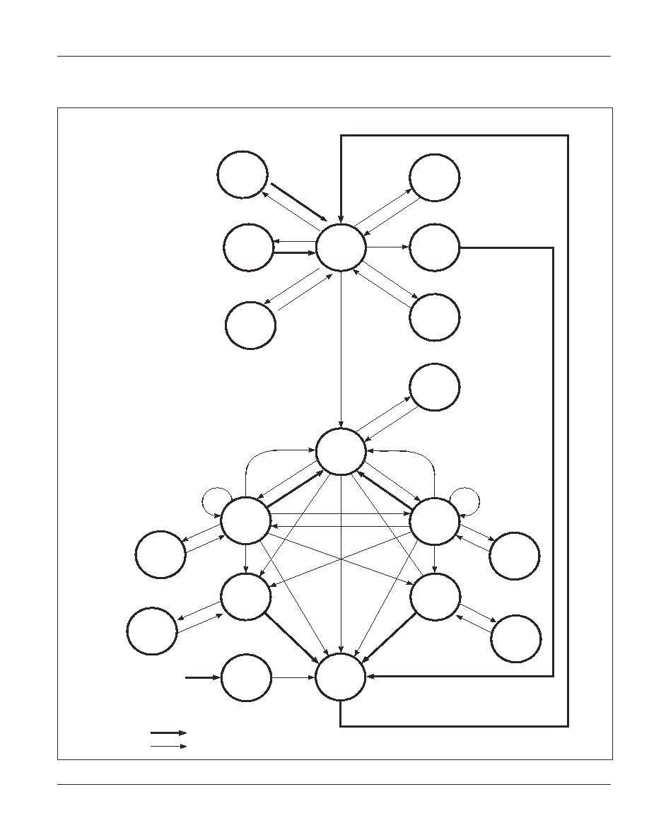
SIMPLIFIED STATE TRANSITION DIAGRAM
(One Bank Operation)
SELF
REFRESH
AUTO
REFRESH
IDLE
POWER
DOWN
ACTIVE
POWER
DOWN
IDLE
MODE
REGISTER
SET
DEEP
POWER
DOWN
READ
BANK
ACTIVE
WRITE
CLOCK
SUSPEND
CLOCK
SUSPEND
READ WITH
AUTO
PRECHARGE
PRE-
CHARGE
POWER ON
WRITE WITH
AUTO
PRECHARGE
CLOCK
SUSPEND
EXT. MODE
REGISTER
SET
Transition due to command input.
Automatic transition following the
completion of command execution.
MRS
SREF entry
SREF exit
REF
CKE_
CKE
ACT
CKE_
CKE
BST
BST
READ
CKE_
CKE
READA
CKE_
CKE
READ
READA
READ
WRITA
WRIT
WRIT
CKE_
CKE
WRITA
CKE_
CKE
WRIT
WRITA
PRE
PRE
READA
PRE
PRE
POWER APPLIED
CLOCK
SUSPEND
EMRS
DPD_
DPD exit

IS42VS16100D
ISSI
Æ
22
Integrated Silicon Solution, Inc. -- www.issi.com --
1-800-379-4774
Rev. 00D
06/30/05
Device Initialization At Power-On
(Power-On Sequence)
As is the case with conventional DRAMs, the IS42VS16100D
product must be initialized by executing a stipulated power-
on sequence after power is applied.
When power is applied, VDD and VDDQ must be driven
High while CLK, CKE,
CS
, DQM, and DQ inputs are
held Low. After stabilization and within 100µs, the CKE
and DQM are driven High, and CLK should begin cycling
according to AC timing specifications. After at least
200µs more has passed with stable NOP or Device
Deselect command cycles, the banks must be
precharged. After the delay t
RP
, the Auto-Refresh
command must be issued at least eight times, followed
by the mode register set command (MRS) to initialize
the mode register.
The mode register set command can be also set before
auto-refresh command.
Mode Register Settings
The mode register set command sets the mode register.
When this command is executed, pins A0 to A9, A10, and
A11 function as data input pins for setting the register, and
this data becomes the device internal OP code. This OP
code has four fields as listed in the table below.
Note that the mode register set command can be executed
only when both banks are in the idle (inactive) state. Wait
at least two cycles after executing a mode register set
command before executing the next command.
CAS
CAS
CAS
CAS
CAS
Latency
During a read operation, the between the execution of the
read command and data output is stipulated as the
CAS
latency. This period can be set using the mode register set
command. The optimal
CAS
latency is determined by the
clock frequency and device speed grade (-7.5/10). See the
"Operating Frequency / Latency Relationships" item for
details on the relationship between the clock frequency and
the
CAS
latency. See the table on the next page for details
on setting the mode register.
Input Pin
Field
A11, A10, A9, A8, A7
Mode Options
A6, A5, A4
CAS
Latency
A3
Burst Type
A2, A1, A0
Burst Length
Burst Length
When writing or reading, data can be input or output data
continuously. In these operations, an address is input only
once and that address is taken as the starting address
internally by the device. The device then automatically
generates the following address. The burst length field in
the mode register stipulates the number of data items input
or output in sequence. In the IS42VS16100D product, a
burst length of 1, 2, 4, 8, or full page can be specified. See
the table on the next page for details on setting the mode
register.
Burst Type
The burst data order during a read or write operation is
stipulated by the burst type, which can be set by the mode
register set command. The IS42VS16100D product supports
sequential mode and interleaved mode burst type settings.
See the table on the next page for details on setting the
mode register. See the "Burst Length and Column Address
Sequence" item for details on DQ data orders in these
modes.
Write Mode
Burst write or single write mode is selected by the OP code
(A11, A10, A9) of the mode register.
A burst write operation is enabled by setting the OP code
(A11, A10, A9) to (0,0,0). A burst write starts on the same
cycle as a write command set. The write start address is
specified by the column address and bank select address
at the write command set cycle.
A single write operation is enabled by setting OP code
(A11, A10, A9) to (0, 0, 1). In a single write operation, data
is only written to the column address and bank select
address specified by the write command set cycle without
regard to the bust length setting.

IS42VS16100D
ISSI
Æ
Integrated Silicon Solution, Inc. -- www.issi.com --
1-800-379-4774
23
Rev. 00D
06/30/05
MODE REGISTER
M2
M1
M0
Sequential
Interleaved
Burst Length
0
0
0
1
1
0
0
1
2
2
0
1
0
4
4
0
1
1
8
8
1
0
0
Reserved
Reserved
1
0
1
Reserved
Reserved
1
1
0
Reserved
Reserved
1
1
1
Full Page
Reserved
A11 A10 A9
A8
A7 A6
A5 A4
A3 A2
A1 A0
WRITE MODE
LT MODE
BT
BL
M3
Type
Burst Type
0
Sequential
1
Interleaved
M6
M5
M4
CAS
CAS
CAS
CAS
CAS
Latency
Latency Mode 0
0
0
Reserved
0
0
1
Reserved
0
1
0
2
0
1
1
3
1
0
0
Reserved
1
0
1
Reserved
1
1
0
Reserved
1
1
1
Reserved
M11
M10
M9
M8
M7
Write Mode
0
0
1
0
0
Burst Read & Single Write
0
0
0
0
0
Burst Read & Burst Write
Address Bus (Ax)
Mode Register (Mx)
Note: Other values for these bits are reserved.
IS42VS16100D
ISSI
Æ
24
Integrated Silicon Solution, Inc. -- www.issi.com --
1-800-379-4774
Rev. 00D
06/30/05
REGISTER DEFINITION
Extended Mode Register
The extended mode register is used to define the specific
SDRAM low-power features. This includes the Temperature
Compensated Self Refresh (TCSR) and Partial Array Self
Refresh (PASR) as shown in EXTENDED MODE REGIS-
TER DEFINITION.
The extended mode register is programmed via the EX-
TENDED LOAD MODE REGISTER command (M11 =1) and
will retain the stored information until it is programmed again
or the device loses power.
Extended Mode register bits M0-M2 controls PASR and M3-
M4 controls (TCSR). M6 - M10 must be programmed to 0.
The Extended Mode Register must be loaded when all
banks are idle and no bursts are in progress. The controller
must initialize the operation after waiting the specified time.
Violating either of these requirements will result in unspeci-
fied operation.
Driver Strength
The bit value of M5 determines the driver strength. If M5 =
0, full driver strength is configured; if M5 =1, half driver
strength is configured. This setting should be based on
application requirements. The default value of M5 is 0.
EXTENDED MODE REGISTER DEFINITION
PASR
M2 M1 M0
Self Refresh Coverage
0
0
0 2 banks
0
0
1 Reserved
0 1 0
1 bank (Bank 0)
0
1
1 Reserved
1
0
0 Reserved
1 0 1
1/2 bank (Bank 0)
1
1 1 0
1/4 bank (Bank 0)
2
1
1
1 Reserved
Address Bus (Ax)
Extended Mode
Register (Mx)
A11 A10
A9 A8 A7 A6 A5 A4 A3 A2 A1 A0
TCSR
M4 M3 Max. Case Temp.
1 0
15
C
0 1
45
C
0 0
70
C
1 1
85
C
M5 Driver Strength
0
Full Strength
1
Half Strength
0
M10-M5
1
M11
Notes:
1. Lower half of Bank 0, such that A10 = 0.
2. Lowest quarter of Bank 0, such that A10 = 0, A9 = 0.
Partial Array Self Refresh (PASR)
To minimize power consumption during Self Refresh mode,
the Extended Mode Register can be configured so that the
SDRAM memory array will be partially refreshed. Any data
outside the partial array refresh coverage area will be lost
during Self Refresh Mode. The values loaded into M2, M1,
and M0 can select Self Refresh coverage for both banks, a
single bank, half of a bank, or a quarter of a bank for the
most power savings. The values M2, M1, and M0 are all 0
by default.
Temperature Compensated Self Refresh
(TCSR)
As the temperature increases, the SDRAM memory cells
must be refreshed more frequently in Self Refresh Mode in
order to retain the data. Without TCSR, an SDRAM in Self
Refresh Mode would refresh itself assuming a worst case
of 85
o
C. However, this frequency would be unnecessarily
high for many occasions in which the ambient temperature
would be much lower. By setting the bit values of M3 and
M4, the refresh rate can be compensated for operating the
device at a temperature lower than the maximum. Minimiz-
ing the refresh rate saves power. The values of M3 and M4
are 0 by default.

IS42VS16100D
ISSI
Æ
Integrated Silicon Solution, Inc. -- www.issi.com --
1-800-379-4774
25
Rev. 00D
06/30/05
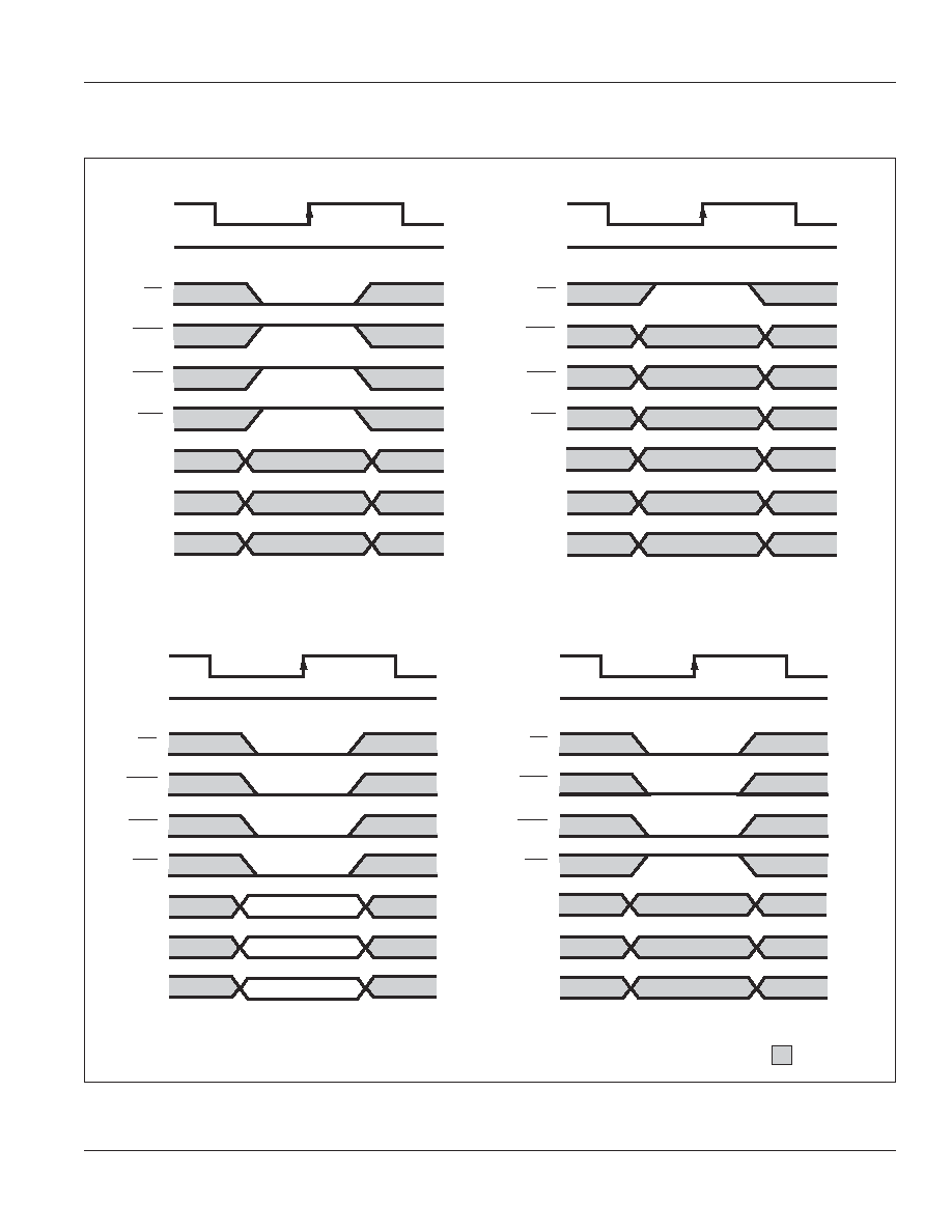
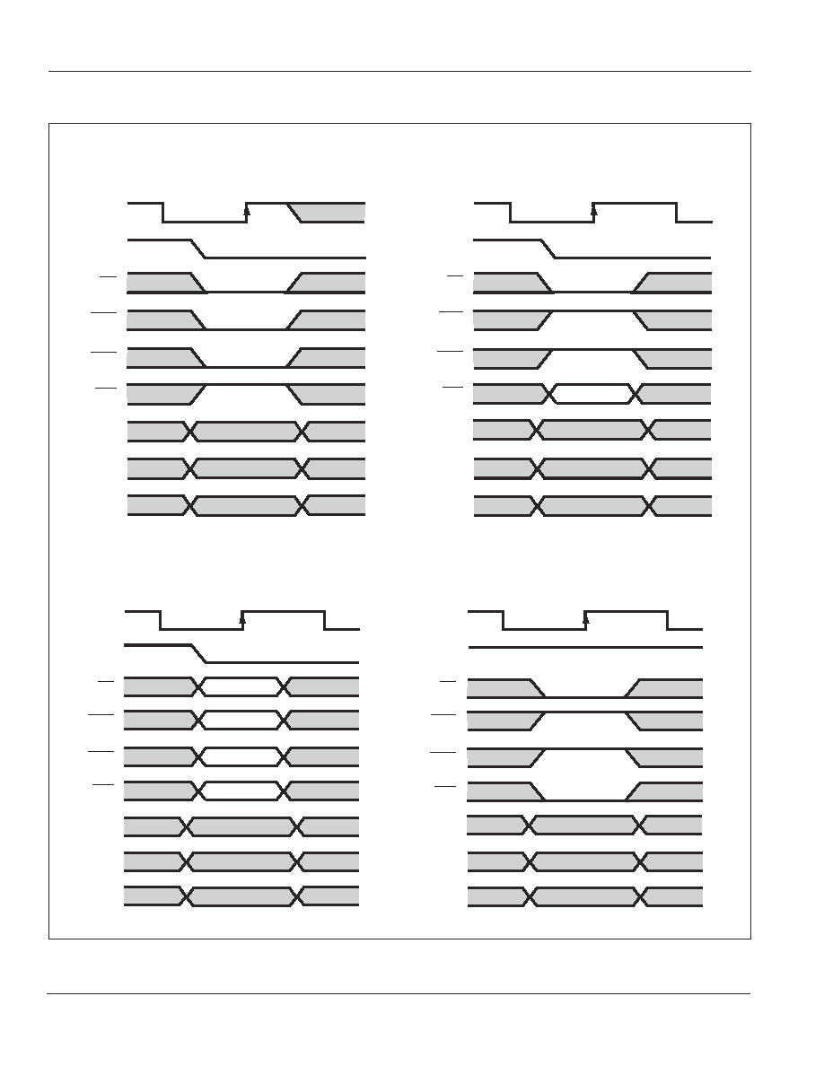
BURST LENGTH AND COLUMN ADDRESS SEQUENCE
Column Address
Address Sequence
Burst Length
A2
A1
A0
Sequential
Interleaved
2
X
X
0
0-1
0-1
X
X
1
1-0
1-0
4
X
0
0
0-1-2-3
0-1-2-3
X
0
1
1-2-3-0
1-0-3-2
X
1
0
2-3-0-1
2-3-0-1
X
1
1
3-0-1-2
3-2-1-0
8
0
0
0
0-1-2-3-4-5-6-7
0-1-2-3-4-5-6-7
0
0
1
1-2-3-4-5-6-7-0
1-0-3-2-5-4-7-6
0
1
0
2-3-4-5-6-7-0-1
2-3-0-1-6-7-4-5
0
1
1
3-4-5-6-7-0-1-2
3-2-1-0-7-6-5-4
1
0
0
4-5-6-7-0-1-2-3
4-5-6-7-0-1-2-3
1
0
1
5-6-7-0-1-2-3-4
5-4-7-6-1-0-3-2
1
1
0
6-7-0-1-2-3-4-5
6-7-4-5-2-3-0-1
1
1
1
7-0-1-2-3-4-5-6
7-6-5-4-3-2-1-0
Full Page
n
n
n
Cn, Cn+1, Cn+2
None
(256)
Cn+3, Cn+4.....
...Cn-1(Cn+255),
Cn(Cn+256).....
Notes:
1. The burst length in full page mode is 256.

IS42VS16100D
ISSI
Æ
26
Integrated Silicon Solution, Inc. -- www.issi.com --
1-800-379-4774
Rev. 00D
06/30/05
BANK SELECT AND PRECHARGE ADDRESS ALLOCATION
Row
X0
--
Row Address
X1
--
Row Address
X2
--
Row Address
X3
--
Row Address
X4
--
Row Address
X5
--
Row Address
X6
--
Row Address
X7
--
Row Address
X8
--
Row Address
X9
--
Row Address
X10
0
Precharge of the Selected Bank (Precharge Command)
Row Address
1
Precharge of Both Banks (Precharge Command)
(Active Command)
X11
0
Bank 0 Selected (Precharge and Active Command)
1
Bank 1 Selected (Precharge and Active Command)
Column
Y0
--
Column Address
Y1
--
Column Address
Y2
--
Column Address
Y3
--
Column Address
Y4
--
Column Address
Y5
--
Column Address
Y6
--
Column Address
Y7
--
Column Address
Y8
--
Don't Care
Y9
--
Don't Care
Y10
0
Auto-Precharge - Disabled
1
Auto-Precharge - Enables
Y11
0
Bank 0 Selected (Read and Write Commands)
1
Bank 1 Selected (Read and Write Commands)
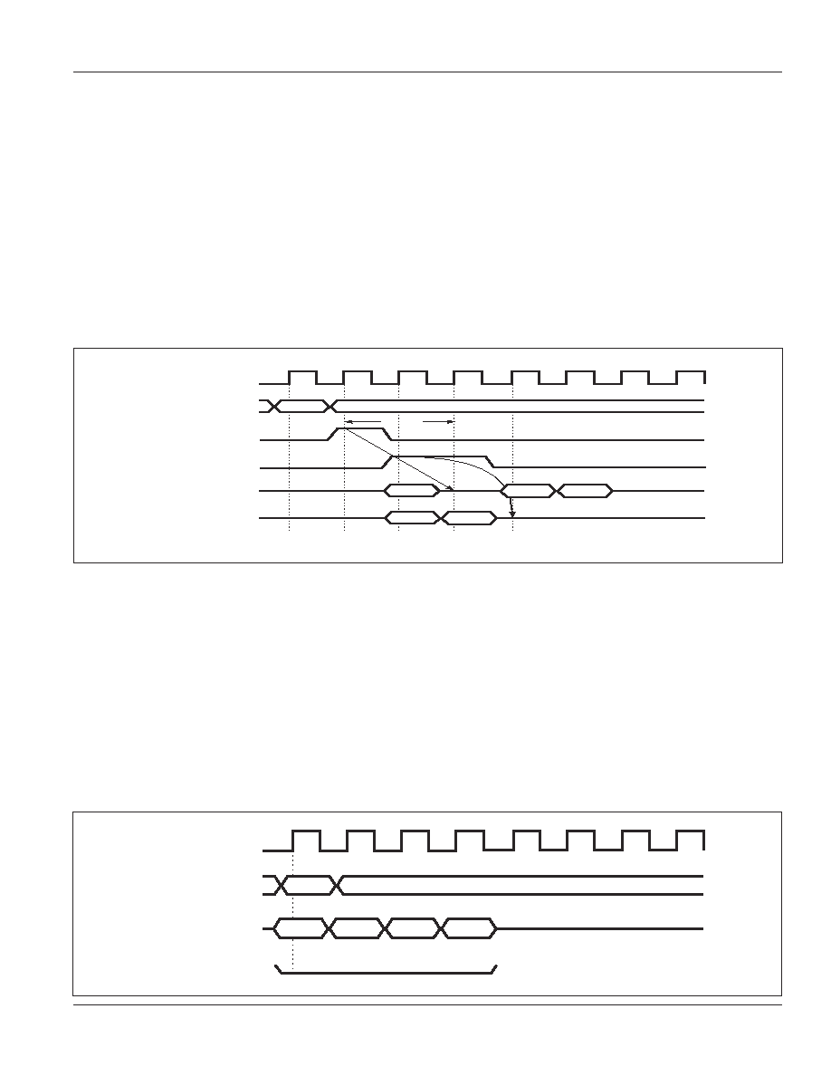
IS42VS16100D
ISSI
Æ
Integrated Silicon Solution, Inc. -- www.issi.com --
1-800-379-4774
27
Rev. 00D
06/30/05
Burst Read
The read cycle is started by executing the read command.
The address provided during read command execution is
used as the starting address. First, the data corresponding
to this address is output in synchronization with the clock
signal after the
CAS
latency period. Next, data corresponding
to an address generated automatically by the device is
output in synchronization with the clock signal.
The output buffers go to the LOW impedance state
CAS
latency minus one cycle after the read command, and go
to the HIGH impedance state automatically after the last
data is output. However, the case where the burst length
is a full page is an exception. In this case the output
buffers must be set to the high impedance state by
executing a burst stop command.
Note that upper byte and lower byte output data can be
masked independently under control of the signals applied
to the U/LDQM pins. The delay period (t
QMD
) is fixed at two,
regardless of the
CAS
latency setting, when this function
is used.
The selected bank must be set to the active state before
executing this command.
CAS
latency = 2, burst length = 4
Burst Write
The write cycle is started by executing the command. The
address provided during write command execution is used
as the starting address, and at the same time, data for this
address is input in synchronization with the clock signal.
Next, data is input in other in synchronization with the clock
signal. During this operation, data is written to address
generated automatically by the device. This cycle
terminates automatically after a number of clock cycles
determined by the stipulated burst length. However, the
case where the burst length is a full page is an exception.
In this case the write cycle must be terminated by executing
a burst stop command. The latency for DQ pin data input
is zero, regardless of the
CAS
latency setting. However, a
wait period (write recovery: t
DPL
) after the last data input is
required for the device to complete the write operation.
Note that the upper byte and lower byte input data can be
masked independently under control of the signals applied
to the U/LDQM pins. The delay period (t
DMD
) is fixed at zero,
regardless of the
CAS
latency setting, when this function
is used.
The selected bank must be set to the active state before
executing this command.
CAS
latency = 2,3, burst length = 4
READ A0
COMMAND
UDQM
LDQM
DQ8-DQ15
DQ0-DQ 7
CLK
D
OUT
A0
t
QMD=2
HI-Z
HI-Z
HI-Z
READ (CA=A, BANK 0)
DATA MASK (LOWER BYTE)
DATA MASK (UPPER BYTE)
D
OUT
A2
D
OUT
A3
D
OUT
A1
D
OUT
A0
BURST LENGTH
WRITE
COMMAND
DQ
CLK
D
IN
0
D
IN
1
D
IN
2
D
IN
3
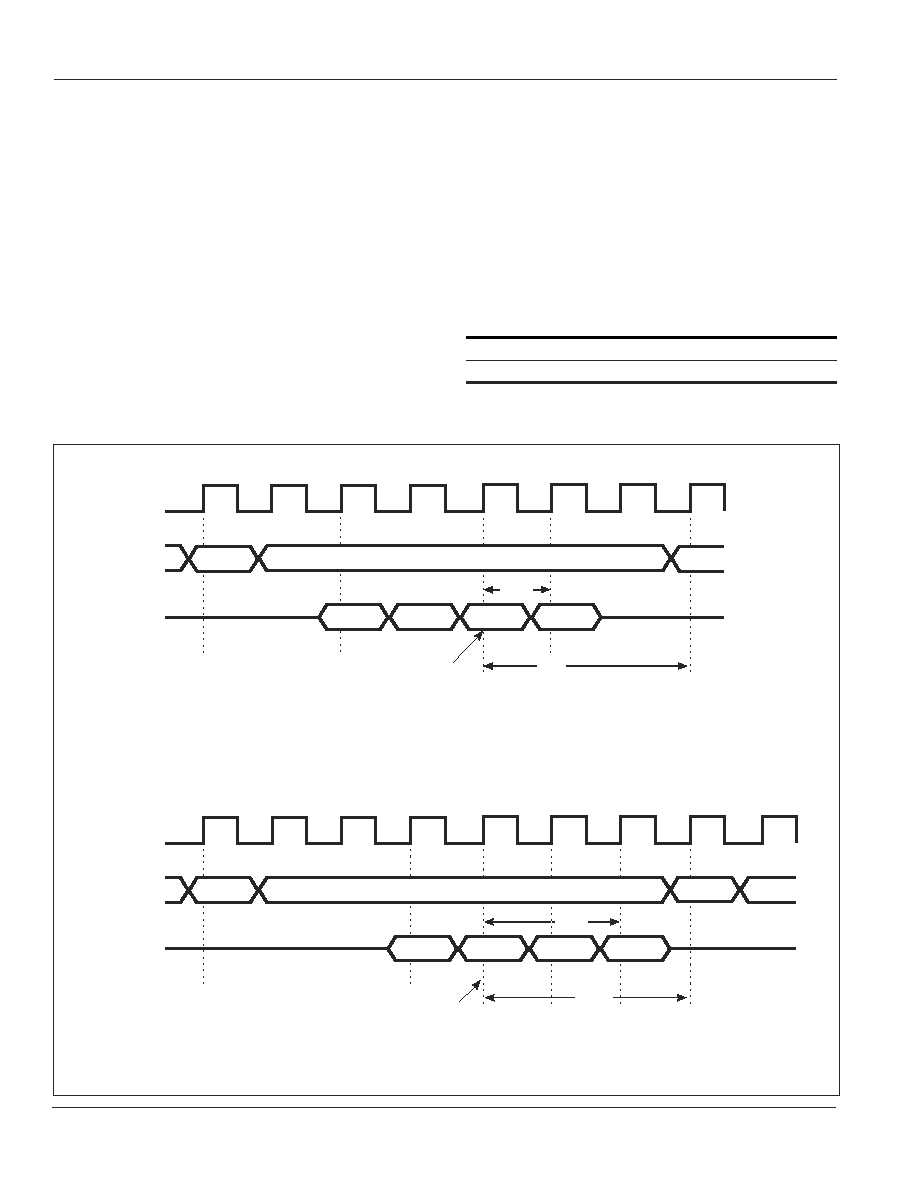
IS42VS16100D
ISSI
Æ
28
Integrated Silicon Solution, Inc. -- www.issi.com --
1-800-379-4774
Rev. 00D
06/30/05
Read With Auto-Precharge
The read with auto-precharge command first executes a
burst read operation and then puts the selected bank in the
precharged state automatically. After the precharge com-
pletes, the bank goes to the idle state. Thus this command
performs a read command and a precharge command in a
single operation.
During this operation, the delay period (t
PQL
) between the
last burst data output and the start of the precharge
operation differs depending on the
CAS
latency setting.
When the
CAS
latency setting is two, the precharge
operation starts on one clock cycle before the last burst
data is output (t
PQL
= ≠1). When the
CAS
latency setting is
three, the precharge operation starts on two clock cycles
before the last burst data is output (t
PQL
= ≠2). Therefore,
the selected bank can be made active after a delay of t
RP
from the start position of this precharge operation.
The selected bank must be set to the active state before
executing this command.
The auto-precharge function is invalid if the burst length is
set to full page.
CAS
CAS
CAS
CAS
CAS
Latency
3
2
t
PQL
≠2
≠1
COMMAND
DQ
CLK
t
RP
t
PQL
READA 0
PRECHARGE START
READ WITH AUTO-PRECHARGE
(BANK 0)
D
OUT
0
D
OUT
1
D
OUT
2
D
OUT
3
COMMAND
DQ
CLK
READA 0
ACT 0
t
RP
PRECHARGE START
READ WITH AUTO-PRECHARGE
(BANK 0)
t
PQL
D
OUT
0
D
OUT
1
D
OUT
2
D
OUT
3
ACT 0
CAS
latency = 2, burstlength = 4
CAS
latency = 3, burstlength = 4
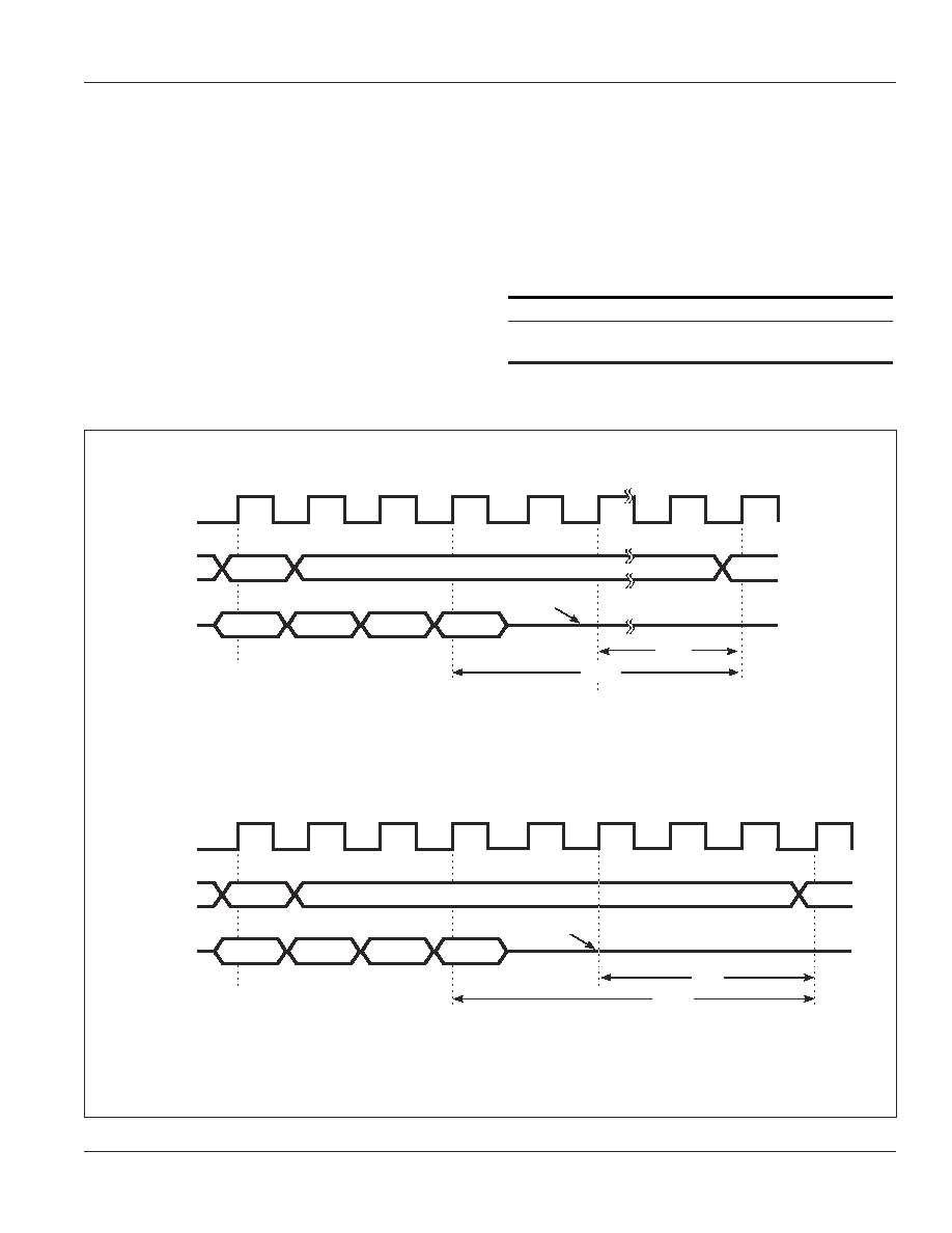
IS42VS16100D
ISSI
Æ
Integrated Silicon Solution, Inc. -- www.issi.com --
1-800-379-4774
29
Rev. 00D
06/30/05
Write With Auto-Precharge
The write with auto-precharge command first executes a
burst write operation and then puts the selected bank in the
precharged state automatically. After the precharge
completes the bank goes to the idle state. Thus this
command performs a write command and a precharge
command in a single operation.
During this operation, the delay period (t
DAL
) between the
last burst data input and the completion of the precharge
operation differs depending on the
CAS
latency setting.
The delay (t
DAL
) is t
RP
plus two CLK periods. That is, the
precharge operation starts two clock periods after the last
burst data input.
Therefore, the selected bank can be made active after a
delay of t
DAL
.
The selected bank must be set to the active state before
executing this command.
The auto-precharge function is invalid if the burst length is
set to full page.
CAS
CAS
CAS
CAS
CAS
Latency
3
2
t
DAL
2CLK
2CLK
+t
RP
+t
RP
t
RP
t
DAL
PRECHARGE START
DQ
WRITE A0
COMMAND
CLK
ACT 0
WRITE WITH AUTO-PRECHARGE
(BANK 0)
t
RP
PRECHARGE START
WRITE A0
COMMAND
DQ
CLK
D
IN
0
D
IN
1
D
IN
2
D
IN
3
ACT 0
WRITE WITH AUTO-PRECHARGE
(BANK 0)
D
IN
0
D
IN
1
D
IN
2
D
IN
3
t
DAL
CAS
latency = 2, burstlength = 4
CAS
latency = 3, burstlength = 4
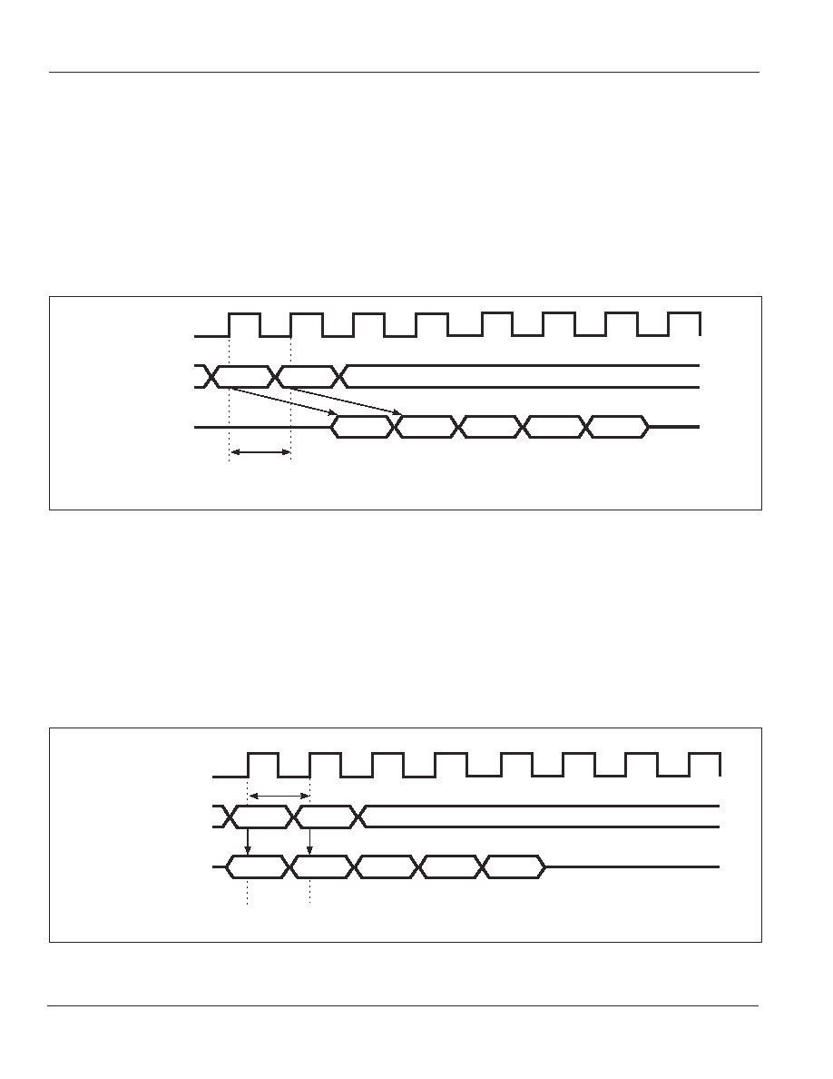
IS42VS16100D
ISSI
Æ
30
Integrated Silicon Solution, Inc. -- www.issi.com --
1-800-379-4774
Rev. 00D
06/30/05
Interval Between Read Command
A new command can be executed while a read cycle is in
progress, i.e., before that cycle completes. When the
second read command is executed, after the
CAS
latency
has elapsed, data corresponding to the new read command
is output in place of the data due to the previous read
command.
The interval between two read command (t
CCD
) must be at
least one clock cycle.
The selected bank must be set to the active state before
executing this command.
Interval Between Write Command
A new command can be executed while a write cycle is in
progress, i.e., before that cycle completes. At the point the
second write command is executed, data corresponding to
the new write command can be input in place of the data
for the previous write command.
The interval between two write commands (t
CCD
) must be
at least one clock cycle.
The selected bank must be set to the active state before
executing this command.
READ A0
READ B0
COMMAND
DQ
CLK
D
OUT
A0
D
OUT
B0
D
OUT
B1
D
OUT
B2
READ (CA=A, BANK 0) READ (CA=B, BANK 0)
t
CCD
D
OUT
B3
CAS
latency = 2, burstlength = 4
WRITE A0
WRITE B0
COMMAND
DQ
CLK
D
IN
A0
D
IN
B0
D
IN
B1
D
IN
B2
D
IN
B3
WRITE (CA=A, BANK 0) WRITE (CA=B, BANK 0)
t
CCD
CAS
latency = 2,3, burstlength = 4
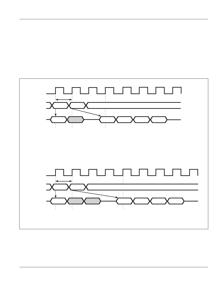
IS42VS16100D
ISSI
Æ
Integrated Silicon Solution, Inc. -- www.issi.com --
1-800-379-4774
31
Rev. 00D
06/30/05
Interval Between Write and Read Commands
A new read command can be executed while a write cycle
is in progress, i.e., before that cycle completes. Data
corresponding to the new read command is output after the
CAS
latency has elapsed from the point the new read
command was executed. The I/On pins must be placed in
the HIGH impedance state at least one cycle before data
is output during this operation.
The interval (t
CCD
) between command must be at least one
clock cycle.
The selected bank must be set to the active state before
executing this command.
DQ
WRITE A0
READ B0
COMMAND
CLK
D
IN
A0
D
OUT
B0
D
OUT
B2
D
OUT
B1
D
OUT
B3
t
CCD
HI-Z
WRITE (CA=A, BANK 0)
READ (CA=B, BANK 0)
DQ
WRITE A0
READ B0
COMMAND
CLK
D
IN
A0
D
OUT
B0
D
OUT
B2
D
OUT
B1
D
OUT
B3
t
CCD
HI-Z
WRITE (CA=A, BANK 0)
READ (CA=B, BANK 0)
CAS
latency = 2, burstlength = 4
CAS
latency = 3, burstlength = 4
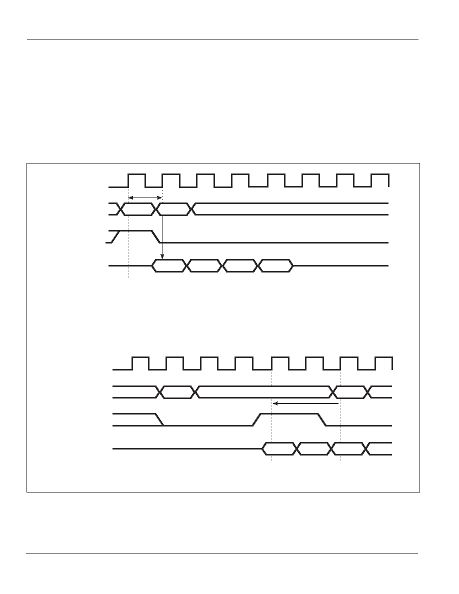
IS42VS16100D
ISSI
Æ
32
Integrated Silicon Solution, Inc. -- www.issi.com --
1-800-379-4774
Rev. 00D
06/30/05
Interval Between Read and Write Commands
A read command can be interrupted and a new write
command executed while the read cycle is in progress,
i.e., before that cycle completes. Data corresponding to
the new write command can be input at the point new
write command is executed. To prevent collision
between input and output data at the DQn pins during
this operation, the
output data must be masked using the U/LDQM pins. The
interval (t
CCD
) between these commands must be at least
one clock cycle.
The selected bank must be set to the active state before
executing this command.
WRITE B0
READ A0
COMMAND
U/LDQM
DQ
CLK
D
IN
B0
D
IN
B2
D
IN
B1
D
IN
B3
t
CCD
HI-Z
READ (CA=A, BANK 0)
WRITE (CA=B, BANK 0)
CAS
latency = 2, 3, burstlength = 4
CAS
latency = 3, burstlength = 4
WRITE B0
READ A0
COMMAND
U/LDQM
DQ
CLK
D
OUT
A0
HI-Z
READ (CA=A, BANK 0)
WRITE (CA=B, BANK 0)
2 clocks
D
OUT
A1
D
IN
B0
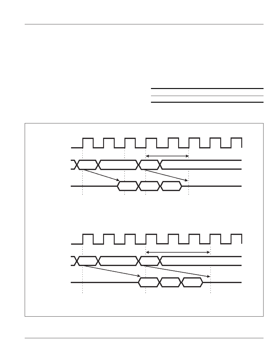
IS42VS16100D
ISSI
Æ
Integrated Silicon Solution, Inc. -- www.issi.com --
1-800-379-4774
33
Rev. 00D
06/30/05
Precharge
The precharge command sets the bank selected by pin A11
to the precharged state. This command can be executed at
a time t
RAS
following the execution of an active command to
the same bank. The selected bank goes to the idle state at
a time t
RP
following the execution of the precharge command,
and an active command can be executed again for that
bank.
If pin A10 is low when this command is executed, the bank
selected by pin A11 will be precharged, and if pin A10 is
HIGH, both banks will be precharged at the same time. This
input to pin A11 is ignored in the latter case.
Read Cycle Interruption
Using the Precharge Command
A read cycle can be interrupted by the execution of the
precharge command before that cycle completes. The
delay time (t
RQL
) from the execution of the precharge
command to the completion of the burst output is the
clock cycle of
CAS
latency.
CAS
CAS
CAS
CAS
CAS
Latency
3
2
t
RQL
3
2
t
RQL
t
RQL
PRE 0
READ A0
COMMAND
DQ
CLK
D
OUT
A0 D
OUT
A1 D
OUT
A2
HI-Z
READ (CA=A, BANK 0)
PRECHARGE (BANK 0)
PRE 0
READ A0
COMMAND
DQ
CLK
D
OUT
A0 D
OUT
A1 D
OUT
A2
HI-Z
READ (CA=A, BANK 0)
PRECHARGE (BANK 0)
CAS
latency = 2, burstlength = 4
CAS
latency = 3, burstlength = 4
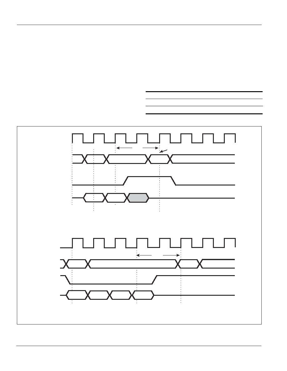
IS42VS16100D
ISSI
Æ
34
Integrated Silicon Solution, Inc. -- www.issi.com --
1-800-379-4774
Rev. 00D
06/30/05
Write Cycle Interruption Using the
Precharge Command
A write cycle can be interrupted by the execution of the
precharge command before that cycle completes. The
delay time (t
WDL
) from the precharge command to the point
where burst input is invalid, i.e., the point where input data
is no longer written to device internal memory is zero clock
cycles regardless of the
CAS
.
To inhibit invalid write, the DQM signal must be asserted
HIGH with the precharge command.
This precharge command and burst write command must
be of the same bank, otherwise it is not precharge interrupt
but only another bank precharge of dual bank operation.
Inversely, to write all the burst data to the device, the
precharge command must be executed after the write
data recovery period (t
DPL
) has elapsed. Therefore, the
precharge command must be executed two clock
cycles following the input of the last burst data item.
CAS
CAS
CAS
CAS
CAS
Latency
3
2
t
WDL
0
0
t
DPL
2
2
PRE 0
WRITE A0
COMMAND
DQM
DQ
CLK
D
IN
A0
D
IN
A1
D
IN
A2
t
WDL
=0
WRITE (CA=A, BANK 0)
PRECHARGE (BANK 0)
MASKED BY DQM
PRE 0
WRITE A0
COMMAND
DQ
CLK
D
IN
A0
D
IN
A1
D
IN
A2
D
IN
A3
t
DPL
WRITE (CA=A, BANK 0)
PRECHARGE (BANK 0)
t
DPL
DQM
CAS
latency = 2, burstlength = 4
CAS
latency = 3, burstlength = 4
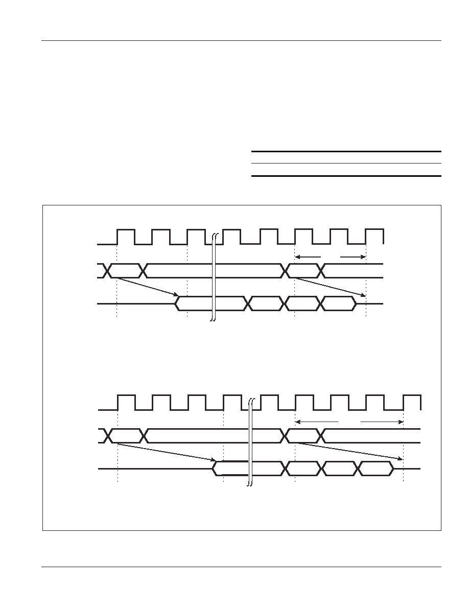
IS42VS16100D
ISSI
Æ
Integrated Silicon Solution, Inc. -- www.issi.com --
1-800-379-4774
35
Rev. 00D
06/30/05
Read Cycle (Full Page) Interruption Using
the Burst Stop Command
The IS42VS16100D can output data continuously from the
burst start address (a) to location a+255 during a read cycle
in which the burst length is set to full page. The
IS42VS16100D repeats the operation starting at the 256th
cycle with the data output returning to location (a) and
continuing with a+1, a+2, a+3, etc. A burst stop command
must be executed to terminate this cycle. A precharge
command must be executed within the ACT to PRE
command period (t
RAS
max.) following the burst stop
command.
After the period (t
RBD
) required for burst data output to
stop following the execution of the burst stop command
has elapsed, the outputs go to the HIGH impedance
state. This period (t
RBD
) is two clock cycle when the
CAS
latency is two and three clock cycle when the
CAS
latency is three.
CAS
CAS
CAS
CAS
CAS
Latency
3
2
t
RBD
3
2
BST
READ A0
COMMAND
DQ
CLK
t
RBD
READ (CA=A, BANK 0)
BURST STOP
HI-Z
D
OUT
A0
D
OUT
An
COMMAND
DQ
CLK
t
RBD
READ A0
READ (CA=A, BANK 0)
BURST STOP
BST
HI-Z
D
OUT
A0 D
OUT
An
D
OUT
An+1
D
OUT
An+2
D
OUT
An+3
D
OUT
An+1
D
OUT
An+2
D
OUT
An+3
CAS
latency = 3, burstlength = 4
CAS
latency = 2, burstlength = 4
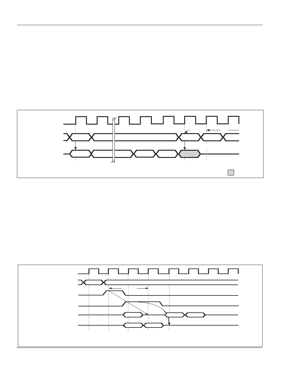
IS42VS16100D
ISSI
Æ
36
Integrated Silicon Solution, Inc. -- www.issi.com --
1-800-379-4774
Rev. 00D
06/30/05
Write Cycle (Full Page) Interruption Using
the Burst Stop Command
The IS42VS16100D can input data continuously from
the burst start address (a) to location a+255 during a
write cycle in which the burst length is set to full page.
The IS42VS16100D repeats the operation starting at the
256th cycle with data input returning to location (a) and
continuing with a+1, a+2, a+3, etc. A burst stop
command must be executed to terminate this cycle. A
precharge command
must be executed within the ACT to PRE command
period (t
RAS
max.) following the burst stop command.
After the period (t
WBD
) required for burst data input to
stop following the execution of the burst stop command
has elapsed, the write cycle terminates. This period
(t
WBD
) is zero clock cycles, regardless of the
CAS
latency.
Burst Data Interruption Using the U/LDQM
Pins (Read Cycle)
Burst data output can be temporarily interrupted (masked)
during a read cycle using the U/LDQM pins. Regardless of
the
CAS
latency, two clock cycles (t
QMD
) after one of the U/
LDQM pins goes HIGH, the corresponding outputs go to the
HIGH impedance state. Subsequently, the outputs are
maintained in the high impedance state as long as that U/
LDQM pin remains HIGH. When the U/LDQM pin goes
LOW, output is resumed at a time t
QMD
later. This output
control operates independently on a byte basis with the
UDQM pin controlling upper byte output (pins
DQ8-DQ15) and the LDQM pin controlling lower byte output
(pins DQ0 to DQ7).
Since the U/LDQM pins control the device output buffers
only, the read cycle continues internally and, in particular,
incrementing of the internal burst counter continues.
CAS
latency = 2, burstlength = 4
READ A0
COMMAND
UDQM
LDQM
DQ8-DQ15
DQ0-DQ 7
CLK
D
OUT
A0
t
QMD=2
HI-Z
HI-Z
HI-Z
READ (CA=A, BANK 0)
DATA MASK (LOWER BYTE)
DATA MASK (UPPER BYTE)
D
OUT
A2
D
OUT
A3
D
OUT
A1
D
OUT
A0
WRITE A0
COMMAND
DQ
CLK
D
IN
A0
D
IN
A1
D
IN
An
D
IN
An+1
D
IN
An+2
t
WBD=0
t
RP
READ (CA=A, BANK 0)
BURST STOP
BST
PRE 0
INVALID DATA
PRECHARGE (BANK 0)
Don't Care
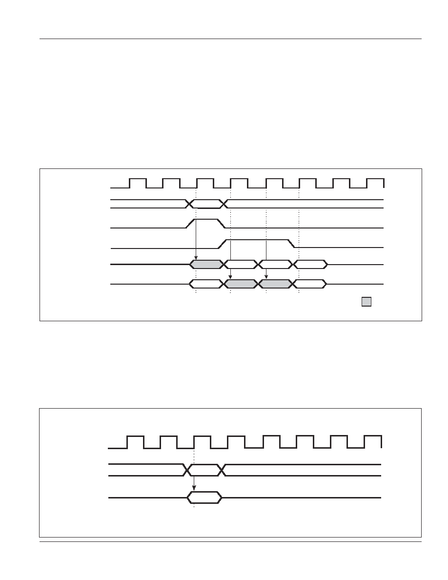
IS42VS16100D
ISSI
Æ
Integrated Silicon Solution, Inc. -- www.issi.com --
1-800-379-4774
37
Rev. 00D
06/30/05
Burst Data Interruption U/LDQM Pins (Write
Cycle)
Burst data input can be temporarily interrupted (muted )
during a write cycle using the U/LDQM pins. Regardless of
the
CAS
latency, as soon as one of the U/LDQM pins goes
HIGH, the corresponding externally applied input data will
no longer be written to the device internal circuits.
Subsequently, the corresponding input continues to be
muted as long as that U/LDQM pin remains HIGH.
The IS42VS16100D will revert to accepting input as soon
as
that pin is dropped to LOW and data will be written to the
device. This input control operates independently on a byte
basis with the UDQM pin controlling upper byte input (pin
DQ8 to DQ15) and the LDQM pin controlling the lower byte
input (pins DQ0 to DQ7).
Since the U/LDQM pins control the device input buffers
only, the cycle continues internally and, in particular,
incrementing of the internal burst counter continues.
Burst Read and Single Write
The burst read and single write mode is set up using the
mode register set command. During this operation, the
burst read cycle operates normally, but the write cycle only
writes a single data item for each write cycle. The
CAS
latency and DQM latency are the same as in normal mode.
WRITE A0
COMMAND
UDQM
LDQM
DQ8-DQ15
DQ0-DQ7
CLK
D
IN
A1
WRITE (CA=A, BANK 0)
DATA MASK (LOWER BYTE)
DATA MASK (UPPER BYTE)
t
DMD=0
D
IN
A2
D
IN
A3
D
IN
A0
D
IN
A3
Don't Care
CAS
latency = 2, 3
CAS
latency = 2, burstlength = 4
WRITE A0
COMMAND
DQ
CLK
D
IN
A0
WRITE (CA=A, BANK 0)
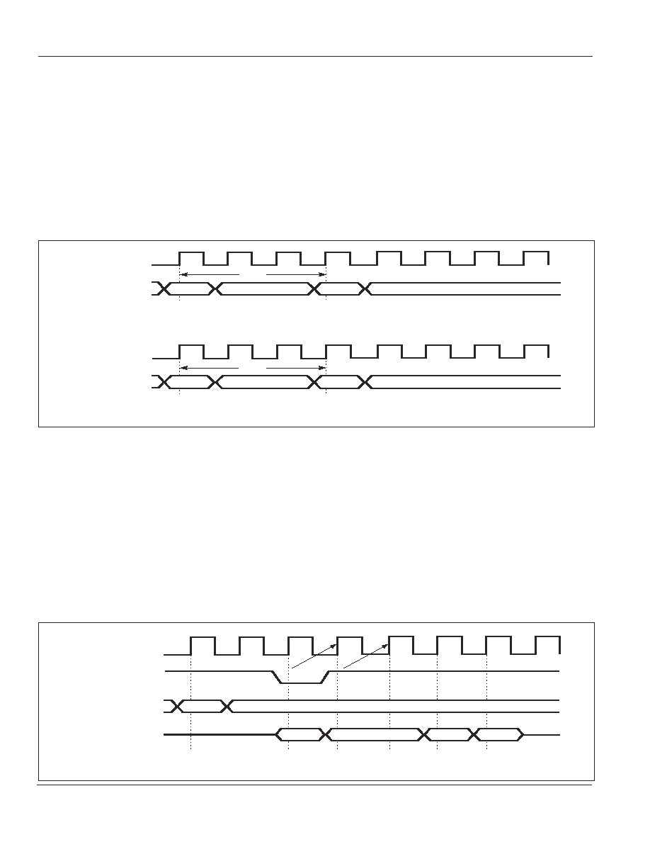
IS42VS16100D
ISSI
Æ
38
Integrated Silicon Solution, Inc. -- www.issi.com --
1-800-379-4774
Rev. 00D
06/30/05
Bank Active Command Interval
When the selected bank is precharged, the period t
RP
has elapsed and the bank has entered the idle state, the
bank can be activated by executing the active
command. If the other bank is in the idle state at that
time, the active command can be executed for that bank
after the period t
RRD
has elapsed. At that point both
banks will be in the active state. When a bank active
command has been executed, a precharge command
must be executed for
that bank within the ACT to PRE command period (t
RAS
max). Also note that a precharge command cannot be
executed for an active bank before t
RAS
(min) has elapsed.
After a bank active command has been executed and the
t
RCD
period has elapsed, read write (including auto-precharge)
commands can be executed for that bank.
ACT 0
ACT 1
COMMAND
CLK
BANK ACTIVE (BANK 0)
BANK ACTIVE (BANK 1)
t
RRD
ACT 0
READ 0
COMMAND
CLK
BANK ACTIVE (BANK 0)
BANK ACTIVE (BANK 0)
t
RCD
CAS
latency = 3
Clock Suspend
When the CKE pin is dropped from HIGH to LOW during a
read or write cycle, the IS42VS16100D enters clock suspend
mode on the next CLK rising edge. This command reduces
the device power dissipation by stopping the device internal
clock. Clock suspend mode continues as long as the CKE
pin remains low. In this state, all inputs other than CKE pin
are invalid and no other commands can be executed. Also,
the device internal states are maintained. When the CKE
pin goes from LOW to HIGH clock suspend mode is
terminated on the next CLK rising edge and device operation
resumes.
The next command cannot be executed until the recovery
period (t
CKA
) has elapsed.
Since this command differs from the self-refresh command
described previously in that the refresh operation is not
performed automatically internally, the refresh operation
must be performed within the refresh period (tref). Thus the
maximum time that clock suspend mode can be held is just
under the refresh cycle time.
READ 0
COMMAND
CKE
DQ
CLK
D
OUT
0
D
OUT
1
D
OUT
2
D
OUT
3
READ (BANK 0)
CLOCK SUSPEND
CAS
latency = 2, burstlength = 4
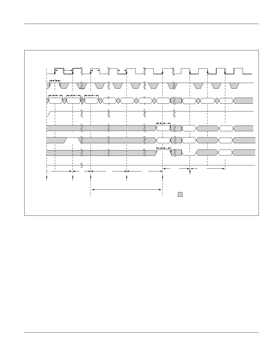
IS42VS16100D
ISSI
Æ
Integrated Silicon Solution, Inc. -- www.issi.com --
1-800-379-4774
39
Rev. 00D
06/30/05
INITIALIZE / LOAD MODE REGISTER AND EXTENDED MODE REGISTER
DON'T CARE
CLK
CKE
COMMAND
DQML
DQMH
A0-A9
A10
A11
DQ
t
CH
t
CL
t
CK
t
CMS
t
CMH
t
CMS
t
CMH
t
CMS
t
CMH
t
CKS
t
CKH
T0 T1 Tn+1 To+1 Tp+1
t
RFC
t
RFC
t
RP
t
AS
t
AH
CODE
CODE
AUTO
REFRESH
AUTO
REFRESH
Load MODE
REGISTER
T = 200µs Min.
Power-up: V
CC
and CLK stable
Precharge
all banks
AUTO REFRESH
AUTO REFRESH
Extended MODE REGISTER
(1,2)
NOP
PRECHARGE NOP NOP
T
CODE
CODE
t
AS
t
AH
ACTIVE
NOP
Load MODE
REGISTER
ALL BANKS
Tp+6
Tp+5
MODE REGISTER
(1,2)
ROW
ROW
BANK
Tp+4
HighZ
At least 8 Auto-Refresh Commands
t
MRD
t
MRD
Notes:
1. The Load Mode Register for both Mode Register / Extended Mode Register and two Auto Refresh Commands can be in
any order. However, all must occur prior to an Active Command.
2. JEDEC and PC100 specify three clocks.
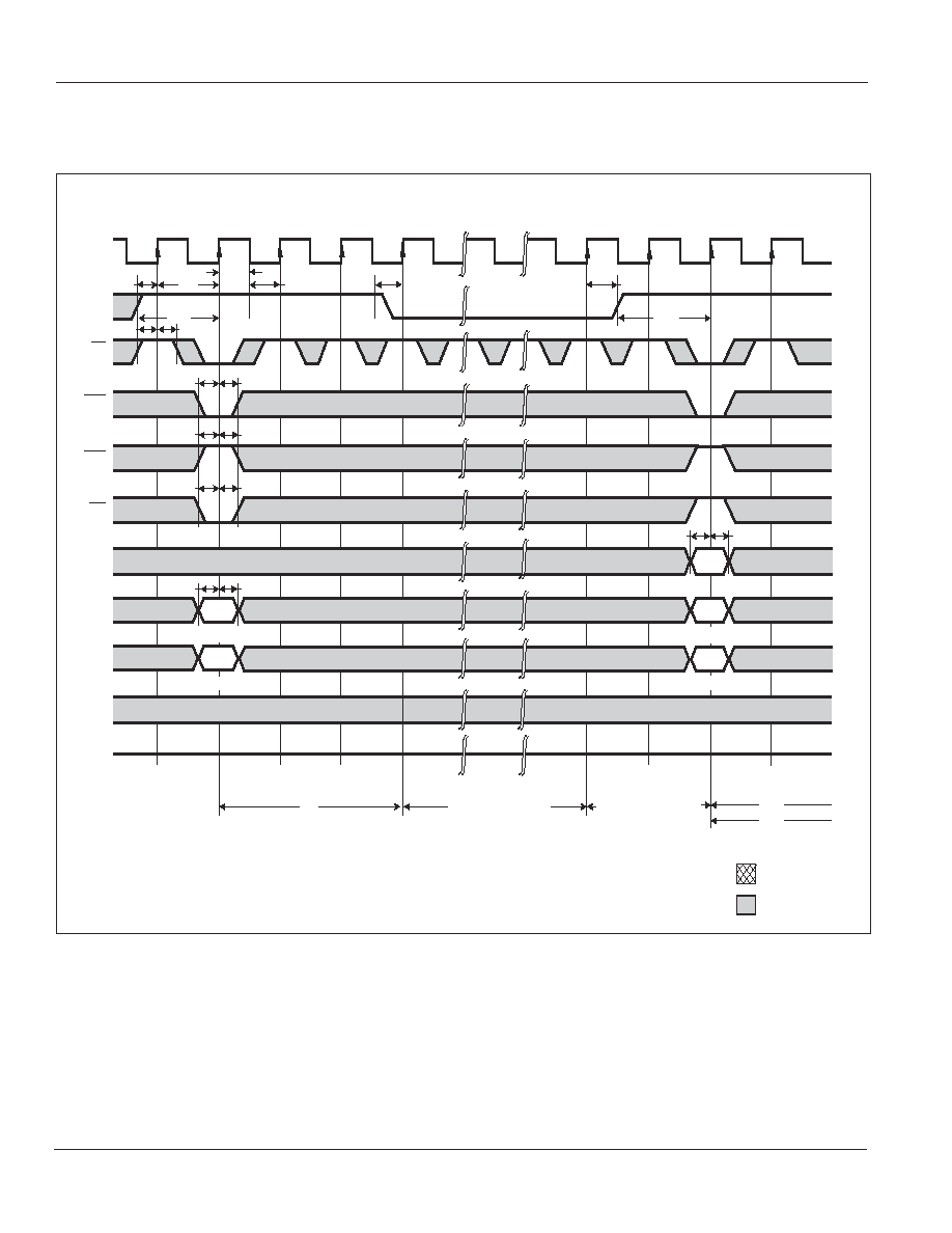
IS42VS16100D
ISSI
Æ
40
Integrated Silicon Solution, Inc. -- www.issi.com --
1-800-379-4774
Rev. 00D
06/30/05
Power-Down Mode Cycle
CLK
CKE
CS
RAS
CAS
WE
A0-A9
A10
A11
DQM
DQ
T0
T1
T2
T3
T4
Tn
Tn+1
Tn+2
Tn+3
t
CK
t
CKS
t
CHI
t
CL
t
CH
t
CS
t
CH
t
CS
t
CH
t
CS
t
CH
t
CS
t
AH
t
AS
ROW
ROW
BANK 1
BANK 0
t
CKS
t
CKH
t
CKA
t
CKA
t
AH
t
AS
t
RP
POWER DOWN MODE
EXIT
POWER DOWN MODE
t
RAS
t
RC
<
ACT
>
<
SBY
>
<
PRE
>
<
PALL
>
BANK 0 & 1
BANK 0 OR 1
BANK 1
BANK 0
CAS
latency = 2, 3
Don't Care
Undefined
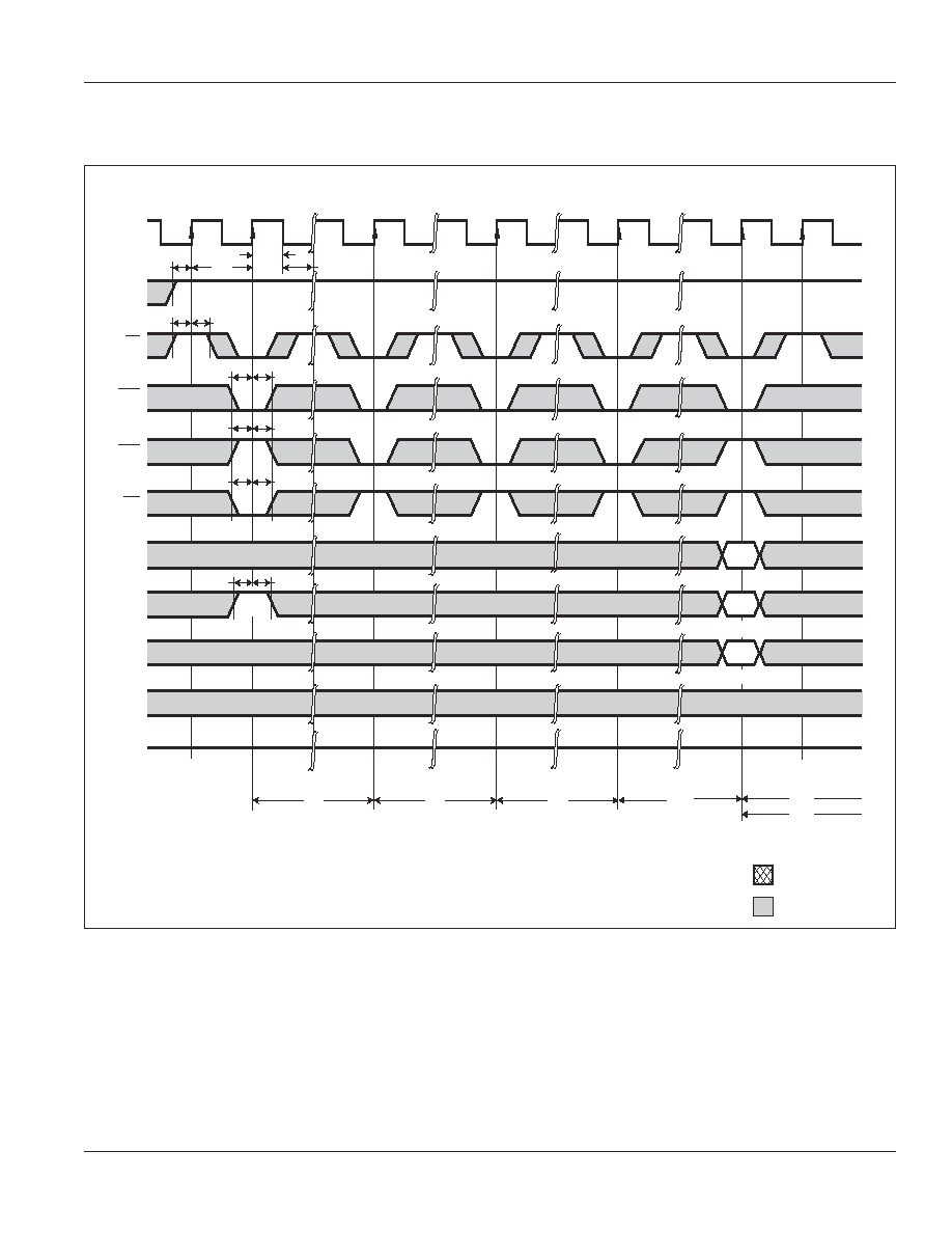
IS42VS16100D
ISSI
Æ
Integrated Silicon Solution, Inc. -- www.issi.com --
1-800-379-4774
41
Rev. 00D
06/30/05
CAS
latency = 2, 3
Auto-Refresh Cycle
CLK
CKE
CS
RAS
CAS
WE
A0-A9
A10
A11
DQM
DQ
T0
T1
T4
Tl
Tm
Tn
Tn+1
t
CK
t
CHI
t
CL
t
CH
t
CS
t
CH
t
CS
t
CH
t
CS
t
CH
t
CS
t
AH
t
AS
BANK 0 & 1
ROW
ROW
BANK 1
BANK 0
t
RP
t
RC
t
RC
t
RC
t
RAS
t
RC
<
ACT
>
<
REF
>
<
REF
>
<
PALL
>
<
REF
>
t
CKS
Don't Care
Undefined
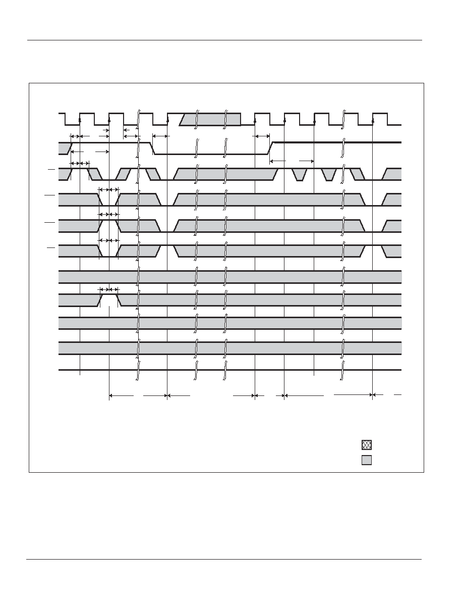
IS42VS16100D
ISSI
Æ
42
Integrated Silicon Solution, Inc. -- www.issi.com --
1-800-379-4774
Rev. 00D
06/30/05
CAS
latency = 2, 3
Self-Refresh Cycle
Don't Care
Undefined
CLK
CKE
CS
RAS
CAS
WE
A0-A9
A10
A11
DQM
DQ
T0
T1
T4
Tm
Tm+2
Tm+1
Tn
t
CK
t
CHI
t
CL
t
CH
t
CS
t
CH
t
CS
t
CH
t
CS
t
CH
t
CS
t
AH
t
AS
BANK 0 & 1
t
CKS
t
CKS
t
CKA
t
CKA
t
RP
SELF REFRESH MODE
EXIT
SELF
REFRESH
t
RC
t
RC
<
REF
>
<
PALL
>
<
SELF
>
t
CKS
Note 1: A8,A9 = Don't Care
.
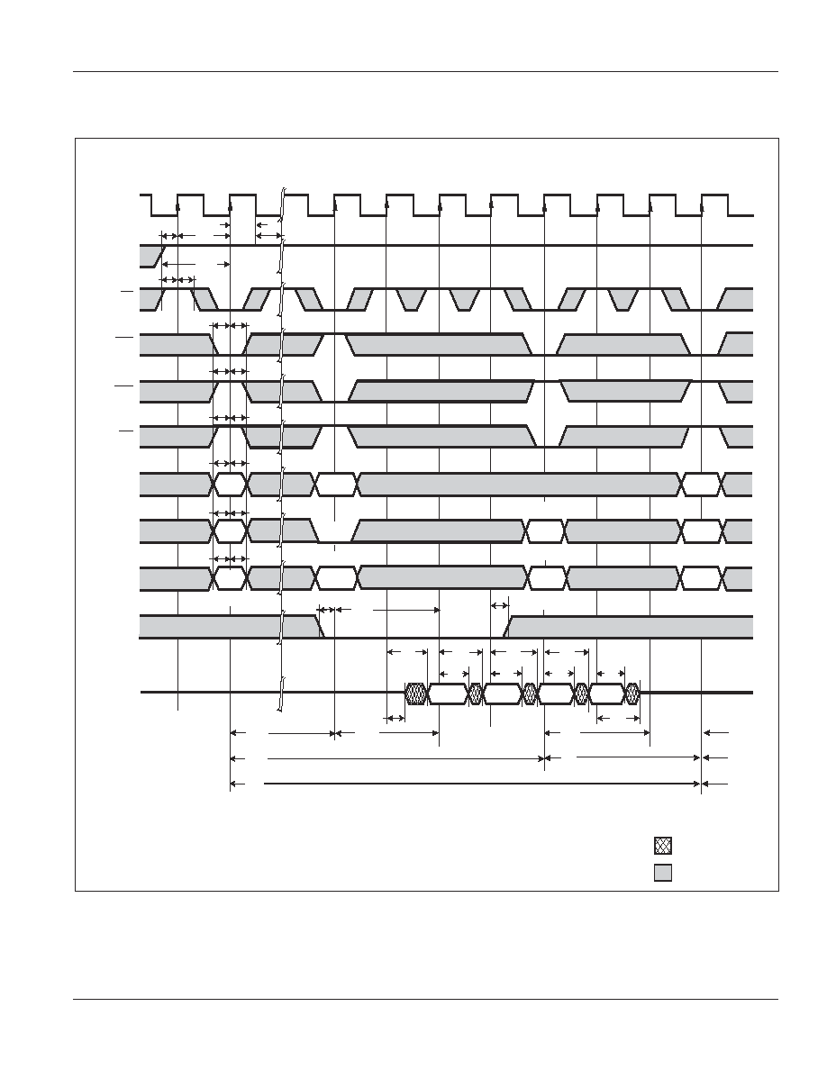
IS42VS16100D
ISSI
Æ
Integrated Silicon Solution, Inc. -- www.issi.com --
1-800-379-4774
43
Rev. 00D
06/30/05
CAS
latency = 2, burstlength = 4
Don't Care
Undefined
CLK
CKE
CS
RAS
CAS
WE
A0-A9
A10
A11
DQM
DQ
T0
T1
T4
T5
T6
T7
T8
T9
T10
T11
t
CK
t
CHI
t
CL
t
CH
t
CS
t
CH
t
CS
t
CH
t
CS
t
CH
t
CS
t
AH
t
AS
BANK 1
BANK 0 AND 1
BANK 0 OR 1
NO PRE
t
AH
t
AS
t
CS
t
AH
t
AS
t
CKS
t
CKA
BANK 0
BANK 0
BANK 1
BANK 1
BANK 0
BANK 1
BANK 0
ROW
COLUMN m
ROW
t
QMD
t
LZ
t
RAS
t
RC
<
ACT
>
<
READ
>
<
ACT
>
<
PRE
>
<
PALL
>
t
RCD
t
CAC
t
RQL
t
RP
t
RCD
t
AC
t
AC
t
OH
t
AC
t
AC
t
OH
t
CH
t
OH
D
OUT
m
D
OUT
m+1
D
OUT
m+2
t
OH
t
HZ
D
OUT
m+3
t
RC
t
RAS
(1)
ROW
ROW
Read Cycle
Note 1: A8,A9 = Don't Care
.
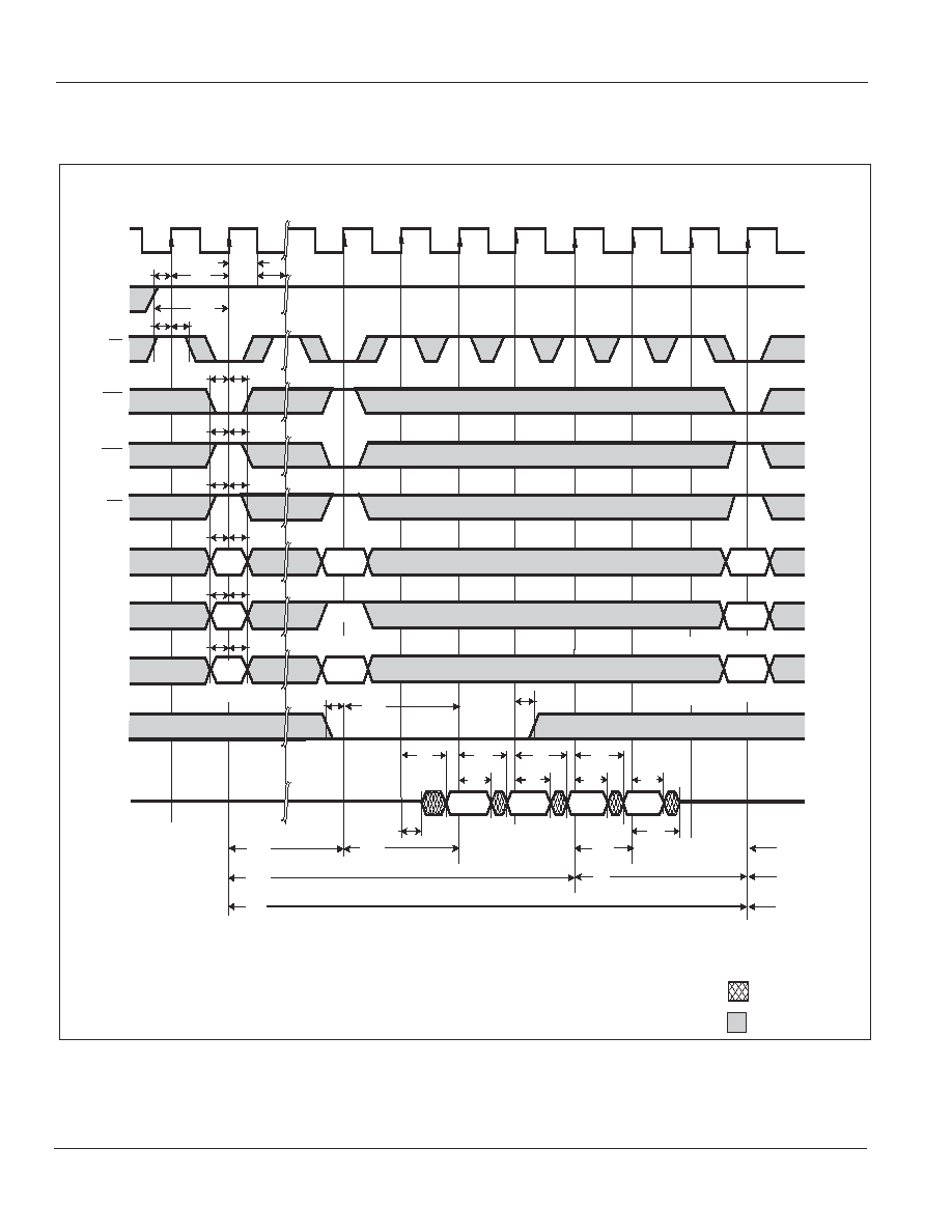
IS42VS16100D
ISSI
Æ
44
Integrated Silicon Solution, Inc. -- www.issi.com --
1-800-379-4774
Rev. 00D
06/30/05
CAS
latency = 2, burstlength = 4
Don't Care
Undefined
Read Cycle / Auto-Precharge
Note 1: A8,A9 = Don't Care
.
CLK
CKE
CS
RAS
CAS
WE
A0-A9
A10
A11
DQM
DQ
T0
T1
T4
T5
T6
T7
T8
T9
T10
T11
t
CK
t
CHI
t
CL
t
CH
t
CS
t
CH
t
CS
t
CH
t
CS
t
CH
t
CS
t
AH
t
AS
BANK 1
AUTO PRE
t
AH
t
AS
t
CS
t
AH
t
AS
t
CKS
t
CKA
BANK 0
BANK 0
BANK 1
ROW
COLUMN m
ROW
t
QMD
t
LZ
t
RAS
t
RC
<
ACT
>
<
READA
>
<
ACT
>
t
RCD
t
CAC
t
PQL
t
RP
t
RCD
t
AC
t
AC
t
OH
t
AC
t
AC
t
OH
t
CH
t
OH
D
OUT
m
D
OUT
m+1
D
OUT
m+2
t
OH
t
HZ
D
OUT
m+3
t
RC
t
RAS
(1)
ROW
ROW
BANK 0
BANK 1
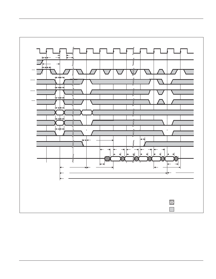
IS42VS16100D
ISSI
Æ
Integrated Silicon Solution, Inc. -- www.issi.com --
1-800-379-4774
45
Rev. 00D
06/30/05
Read Cycle / Full Page
CLK
CKE
CS
RAS
CAS
WE
A0-A9
A10
A11
DQM
DQ
T0
T1
T4
T5
T6
T7
Tp
Tp+1
Tp+2
Tp+3
t
CK
t
CHI
t
CL
t
CH
t
CS
t
CH
t
CS
t
CH
t
CS
t
CH
t
CS
t
AH
t
AS
NO PRE
t
AH
t
AS
t
CS
t
AH
t
AS
t
CKS
t
CKA
BANK 0
BANK 0
BANK 0 OR 1
BANK 0
ROW
COLUMN
ROW
t
QMD
t
LZ
t
RAS
t
RC
(BANK 0)
<
ACT 0
>
<
READ0
>
<
BST
>
<
PRE 0
>
t
RCD
t
CAC
(BANK 0)
t
RBD
t
AC
t
AC
t
OH
t
AC
t
AC
t
AC
t
OH
t
CH
t
OH
D
OUT
0m
D
OUT
0m+1
D
OUT
0m-1
t
OH
t
HZ
t
OH
D
OUT
0m
D
OUT
0m+1
t
RP
(BANK 0)
(1)
CAS
latency = 2, burstlength = full page
Don't Care
Undefined
Note 1: A8,A9 = Don't Care
.
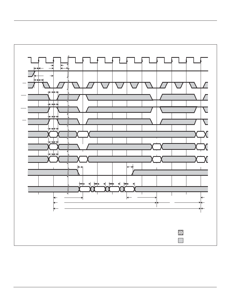
IS42VS16100D
ISSI
Æ
46
Integrated Silicon Solution, Inc. -- www.issi.com --
1-800-379-4774
Rev. 00D
06/30/05
Write Cycle
CLK
CKE
CS
RAS
CAS
WE
A0-A9
A10
A11
DQM
DQ
T0
T1
T4
T5
T6
T8
T7
T9
T10
T11
T12
t
CK
t
CHI
t
CL
t
CH
t
CS
t
CH
t
CS
t
CH
t
CS
t
CH
t
CS
t
AH
t
AS
BANK 1
BANK 0
BANK 0 AND 1
NO PRE
t
CH
t
AH
t
AS
t
CS
t
DS
t
DS
t
DS
t
DS
t
DH
t
RAS
t
RC
<
PRE
>
<
PALL
>
<
ACT
>
<
ACT
>
<
WRIT
>
t
AH
t
AS
t
CKS
t
CKA
ROW
ROW
ROW
COLUMN m
ROW
t
RCD
t
DH
t
DH
t
DH
t
RP
t
DPL
t
RCD
t
RAS
t
RC
D
IN
m
D
IN
m+2
D
IN
m+1
D
IN
m+3
BANK 1
BANK 0
BANK 1
BANK 0
(1)
BANK 0 OR 1
BANK 1
BANK 0
CAS
latency = 2, burstlength = 4
Don't Care
Undefined
Note 1: A8,A9 = Don't Care
.
IS42VS16100D
ISSI
Æ
Integrated Silicon Solution, Inc. -- www.issi.com --
1-800-379-4774
47
Rev. 00D
06/30/05
Write Cycle / Auto-Precharge
CLK
CKE
CS
RAS
CAS
WE
A0-A9
A10
A11
DQM
DQ
T0
T1
T4
T5
T6
T8
T7
T9
T12
t
CK
t
CHI
t
CL
t
CH
t
CS
t
CH
t
CS
t
CH
t
CS
t
CH
t
CS
t
AH
t
AS
BANK 1
BANK 0
AUTO PRE
t
CH
t
AH
t
AS
t
CS
t
DS
t
DS
t
DS
t
DS
t
DH
t
RAS
t
RC
<
ACT
>
<
ACT
>
<
WRITA
>
t
AH
t
AS
t
CKS
t
CKA
ROW
ROW
ROW
COLUMN m
ROW
t
RCD
t
DH
t
DH
t
DH
t
RP
t
DAL
t
RCD
t
RAS
t
RC
D
IN
m
D
IN
m+2
D
IN
m+1
D
IN
m+3
BANK 1
BANK 0
BANK 1
BANK 0
(1)
CAS
latency = 2, burstlength = 4
Don't Care
Undefined
Note 1: A8,A9 = Don't Care
.
IS42VS16100D
ISSI
Æ
48
Integrated Silicon Solution, Inc. -- www.issi.com --
1-800-379-4774
Rev. 00D
06/30/05
Write Cycle / Full Page
CLK
CKE
CS
RAS
CAS
WE
A0-A9
A10
A11
DQM
DQ
T0
T1
T4
T5
T6
T260
T259
T261
T262
T263
t
CK
t
CHI
t
CL
t
CH
t
CS
t
CH
t
CS
t
CH
t
CS
t
CH
t
CS
t
AH
t
AS
NO PRE
t
AH
t
AS
t
CS
t
AH
t
AS
t
CKS
t
CKA
BANK 0
BANK 0
BANK 0 OR 1
BANK 0
ROW
COLUMN m
ROW
t
RAS
t
RC
<
ACT 0
>
<
WRIT0
>
<
BST
>
<
PRE 0
>
t
RCD
t
CH
t
DPL
t
RP
t
DS
t
DS
t
DS
t
DS
t
DH
t
DH
t
DH
t
DH
D
IN
0m
D
IN
0m+2
D
IN
0m+1
D
IN
0m-1
D
IN
0m
(1)
CAS
latency = 2, burst length = full page
Don't Care
Undefined
Note 1: A8,A9 = Don't Care
.
IS42VS16100D
ISSI
Æ
Integrated Silicon Solution, Inc. -- www.issi.com --
1-800-379-4774
49
Rev. 00D
06/30/05
Write Cycle / Ping-Pong Operation
CLK
CKE
CS
RAS
CAS
WE
A0-A9
A10
A11
DQM
DQ
T0
T1
T4
T5
T6
T7
T8
T9
T10
T11
T12
t
CK
t
CHI
t
CL
t
CH
t
CS
t
CH
t
CS
t
CH
t
CS
t
CH
t
CS
t
AH
t
AS
BANK 0
BANK 0
BANK 0
BANK 1
BANK 1
BANK 0 OR 1
NO PRE
NO PRE
t
CH
t
AH
t
AS
t
CS
t
DS
t
DS
t
RCD
(BANK 0)
t
RAS
(BANK 0)
<
ACT 0
>
<
ACT 1
>
<
WRIT 0
>
<
WRITA 0
>
<
WRITA 1
>
<
WRIT 1
>
<
PRE 0
>
<
ACT 0
>
t
AH
t
AS
t
CKS
t
CKA
ROW
ROW
ROW
ROW
ROW
COLUMN
COLUMN
AUTO PRE
AUTO PRE
ROW
t
RCD
(BANK 1)
t
RAS
(BANK 1)
t
RC
(BANK 1)
t
RC
(BANK 0)
t
RCD
(BANK 0)
t
RP
(BANK 0)
t
RAS
(BANK 0)
t
RC
(BANK 0)
t
RRD
(BANK 0 TO 1)
t
DPL
t
DPL
t
DH
t
DH
t
DS
t
DH
t
DH
D
IN
0m
t
DS
t
DS
t
DH
t
DS
t
DH
t
DH
t
DH
t
DS
t
DS
D
IN
0m+1
D
IN
0m+2
D
IN
0m+3
D
IN
1m
D
IN
1m+1
D
IN
1m+2
D
IN
1m+3
(1)
(1)
BANK 0
Don't Care
Undefined
CAS
latency = 2, burst length = 2
Note 1: A8,A9 = Don't Care
.
IS42VS16100D
ISSI
Æ
50
Integrated Silicon Solution, Inc. -- www.issi.com --
1-800-379-4774
Rev. 00D
06/30/05
Read Cycle / Page Mode
CLK
CKE
CS
RAS
CAS
WE
A0-A9
A10
A11
DQM
DQ
T0
T1
T4
T5
T6
T7
T8
T9
T10
T11
t
CK
t
CHI
t
CL
t
CH
t
CS
t
CH
t
CS
t
CH
t
CS
t
CH
t
CS
t
AH
t
AS
BANK 1
BANK 0
BANK 0
BANK 0
BANK 0
BANK 1
BANK 0 OR 1
BANK 0 AND 1
BANK 1
t
CH
t
AH
t
AS
t
LZ
t
CS
t
RAS
t
RC
<
ACT
>
<
READ
>
<
READA
>
<
READ
>
<
READ
>
<
PALL
>
<
PRE
>
t
AH
t
AS
t
CKS
t
CKA
ROW
COLUMN m
COLUMN n
COLUMN o
NO PRE
NO PRE
NO PRE
AUTO PRE
ROW
t
RCD
t
CAC
t
CAC
t
CAC
t
RQL
t
HZ
t
RP
t
QMD
BANK 1
BANK 0
BANK 1
t
AC
t
AC
t
OH
t
AC
t
AC
t
AC
t
AC
t
OH
t
OH
t
OH
t
OH
t
OH
D
OUT
m
D
OUT
m+1
D
OUT
n
D
OUT
n+1
D
OUT
o
D
OUT
o+1
(1)
(1)
(1)
Don't Care
Undefined
CAS
latency = 2, burst length = 2
Note 1: A8,A9 = Don't Care
.
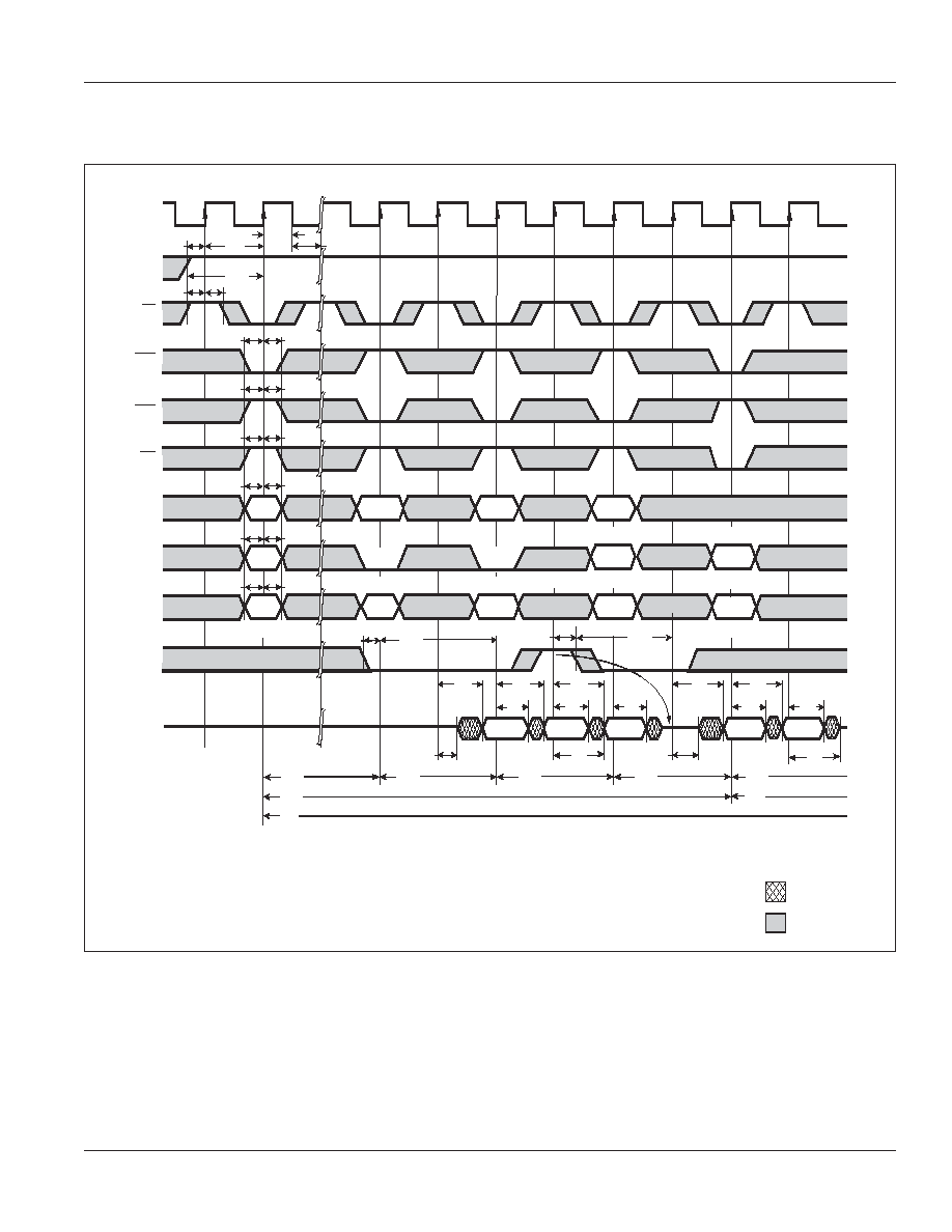
IS42VS16100D
ISSI
Æ
Integrated Silicon Solution, Inc. -- www.issi.com --
1-800-379-4774
51
Rev. 00D
06/30/05
Read Cycle / Page Mode; Data Masking
CLK
CKE
CS
RAS
CAS
WE
A0-A9
A10
A11
DQM
DQ
T0
T1
T4
T5
T6
T7
T8
T9
T10
T11
t
CK
t
CHI
t
CL
t
CH
t
CS
t
CH
t
CS
t
CH
t
CS
t
CH
t
CS
t
AH
t
AS
BANK 1
BANK 0
BANK 0
BANK 0
BANK 0
BANK 1
BANK 0 OR 1
BANK 0 AND 1
NO PRE
BANK 1
t
QMD
t
AH
t
AS
t
LZ
t
CS
t
RAS
t
RC
<
ACT
>
<
READ
>
<
READA, ENB
>
<
READ, ENB
>
<
MASK
>
<
PALL
>
<
PRE
>
t
AH
t
AS
t
CKS
t
CKA
ROW
COLUMN m
COLUMN n
COLUMN o
NO PRE
NO PRE
NO PRE
AUTO PRE
ROW
t
CH
t
RCD
t
CAC
t
CAC
t
CAC
t
RQL
t
HZ
t
HZ
t
RP
t
QMD
BANK 1
BANK 0
BANK 1
t
AC
t
LZ
t
AC
t
OH
t
AC
t
AC
t
AC
t
OH
t
OH
t
OH
t
OH
D
OUT
m
D
OUT
m+1
D
OUT
n
D
OUT
o
D
OUT
o+1
(1)
(1)
(1)
Don't Care
Undefined
CAS
latency = 2, burst length = 2
Note 1: A8,A9 = Don't Care
.
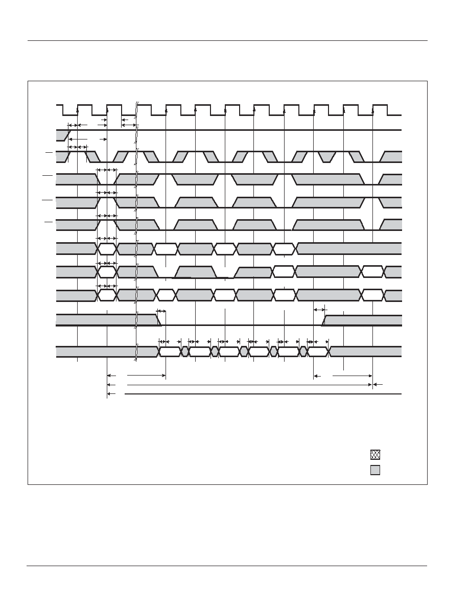
IS42VS16100D
ISSI
Æ
52
Integrated Silicon Solution, Inc. -- www.issi.com --
1-800-379-4774
Rev. 00D
06/30/05
Write Cycle / Page Mode
CLK
CKE
CS
RAS
CAS
WE
A0-A9
A10
A11
DQM
DQ
T0
T1
T4
T5
T6
T7
T8
T9
T10
T11
t
CK
t
CHI
t
CL
t
CH
t
CS
t
CH
t
CS
t
CH
t
CS
t
CH
t
CS
t
AH
t
AS
BANK 1
BANK 0
BANK 0
BANK 0
BANK 0
BANK 1
BANK 0 OR 1
BANK 0 AND 1
BANK 1
t
CH
t
AH
t
AS
t
CS
t
RAS
t
RC
<
ACT
>
<
WRIT
>
<
WRITA
>
<
WRIT
>
<
WRIT
>
<
PALL
>
<
PRE
>
t
AH
t
AS
t
CKS
t
CKA
ROW
COLUMN m
COLUMN n
COLUMN o
NO PRE
NO PRE
NO PRE
AUTO PRE
ROW
t
RCD
t
DPL
t
RP
BANK 1
BANK 0
BANK 1
t
DS
t
DS
t
DS
t
DS
t
DH
t
DS
t
DH
t
DH
t
DH
t
DS
t
DH
t
DH
D
IN
m
D
IN n
D
IN
m+1
D
IN
n+1
D
IN
o
D
IN
o+1
(1)
(1)
(1)
Don't Care
Undefined
CAS
latency = 2, burst length = 2
Note 1: A8,A9 = Don't Care
.
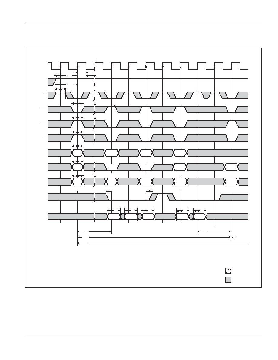
IS42VS16100D
ISSI
Æ
Integrated Silicon Solution, Inc. -- www.issi.com --
1-800-379-4774
53
Rev. 00D
06/30/05
Write Cycle / Page Mode; Data Masking
CLK
CKE
CS
RAS
CAS
WE
A0-A9
A10
A11
DQM
DQ
T0
T1
T4
T5
T6
T7
T8
T9
T10
T11
t
CK
t
CHI
t
CL
t
CH
t
CS
t
CH
t
CS
t
CH
t
CS
t
CH
t
CS
t
AH
t
AS
BANK 1
BANK 0
BANK 0
BANK 0
BANK 0
BANK 1
BANK 1OR 0
BANK 0 AND 1
BANK 1
t
CH
t
AH
t
AS
t
CS
t
RAS
t
RC
<
ACT
>
<
WRIT
>
<
WRIT
>
<
WRITA
>
<
WRIT
>
<
MASK
>
<
PALL
>
<
PRE
>
t
AH
t
AS
t
CKS
t
CKA
ROW
COLUMN m
COLUMN n
COLUMN o
NO PRE
NO PRE
NO PRE
AUTO PRE
ROW
t
RCD
t
DPL
t
RP
BANK 1
BANK 0
BANK 1
t
DS
t
DS
t
DS
t
DH
t
DS
t
DH
t
DH
t
DH
t
DS
t
DH
D
IN
m
D
IN n
D
IN
m+1
D
IN
o
D
IN
o+1
(1)
(1)
(1)
Don't Care
Undefined
CAS
latency = 2, burst length = 2
Note 1: A8,A9 = Don't Care
.

IS42VS16100D
ISSI
Æ
54
Integrated Silicon Solution, Inc. -- www.issi.com --
1-800-379-4774
Rev. 00D
06/30/05
Read Cycle / Clock Suspend
CLK
CKE
CS
RAS
CAS
WE
A0-A9
A10
A11
DQM
DQ
T0
T1
T4
T5
T6
T7
T8
T9
T10
T11
t
CK
t
CHI
t
CL
t
CH
t
CS
t
CH
t
CS
t
CH
t
CS
t
CH
t
CS
t
AH
t
AS
NO PRE
AUTO PRE
t
AH
t
AS
t
CS
t
CKH
t
AH
t
AS
t
CKS
t
CKA
t
CKS
BANK 1
BANK 0
BANK 1
BANK 1
BANK 0
BANK 0
BANK 1
BANK 0
BANK 0 AND 1
BANK 0 OR 1
ROW
ROW
ROW
COLUMN m
ROW
t
QMD
t
LZ
t
RAS
t
RC
t
RC
<
ACT 0
>
<
ACT
>
<
READ
>
<
READ A
>
<
SPND
>
<
SPND
>
<
PRE
>
<
PALL
>
t
RCD
t
CAC
t
AC
t
AC
t
OH
t
OH
t
CH
D
OUT
m
D
OUT
m+1
t
HZ
t
RP
t
RAS
(1)
Don't Care
Undefined
CAS
latency = 2, burst length = 2
Note 1: A8,A9 = Don't Care
.
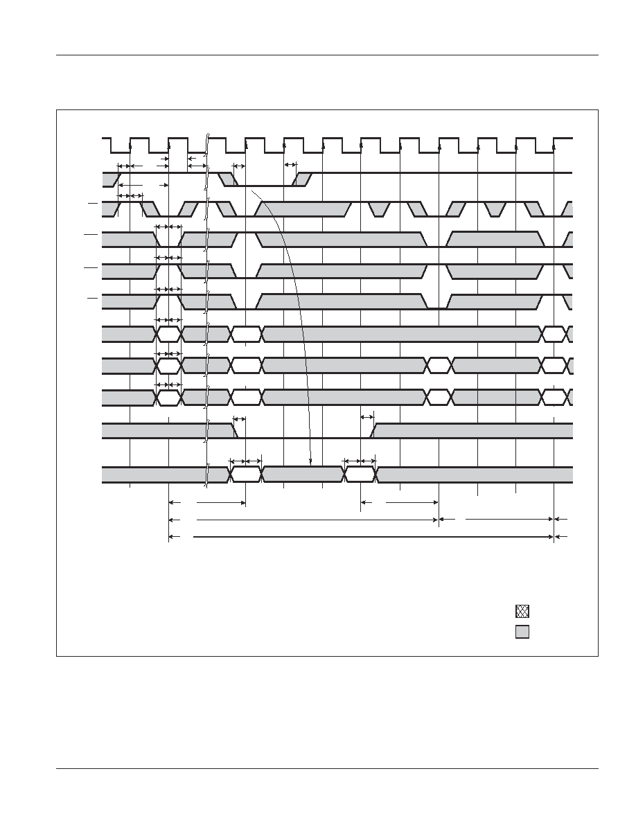
IS42VS16100D
ISSI
Æ
Integrated Silicon Solution, Inc. -- www.issi.com --
1-800-379-4774
55
Rev. 00D
06/30/05
Write Cycle / Clock Suspend
CLK
CKE
CS
RAS
CAS
WE
A0-A9
A10
A11
DQM
DQ
T0
T1
T4
T5
T6
T7
T8
T9
T10
T11 T12
t
CK
t
CHI
t
CL
t
CH
t
CS
t
CH
t
CS
t
CH
t
CS
t
CH
t
CS
t
AH
t
AS
NO PRE
AUTO PRE
t
AH
t
AS
t
CS
t
CKH
t
AH
t
AS
t
CKS
t
CKA
t
CKS
BANK 1
BANK 0
BANK 1
BANK 0
BANK 1
BANK 0
BANK 0 AND 1
BANK 0 OR 1
ROW
ROW
ROW
COLUMN m
ROW
t
DS
t
RAS
t
RC
t
RC
<
ACT
>
<
ACT
>
<
WRIT, SPND
>
<
WRITA, SPND
>
<
SPND
>
<
PRE
>
<
PALL
>
t
RCD
t
CH
t
DH
t
DH
t
DS
t
DPL
t
RP
t
RAS
D
IN
m
D
IN
m+1
(1)
BANK 1
BANK 0
Don't Care
Undefined
CAS
latency = 2, burst length = 2
Note 1: A8,A9 = Don't Care
.
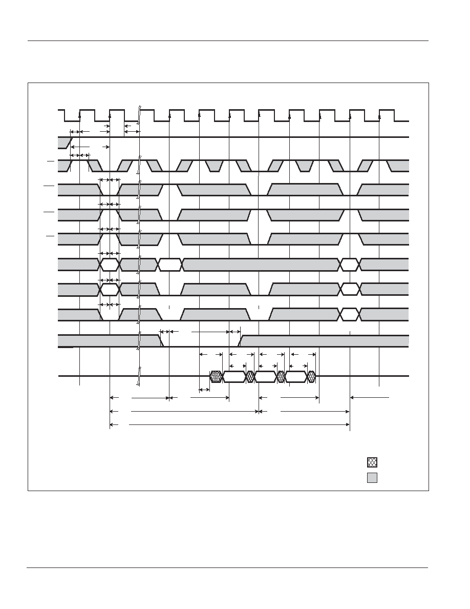
IS42VS16100D
ISSI
Æ
56
Integrated Silicon Solution, Inc. -- www.issi.com --
1-800-379-4774
Rev. 00D
06/30/05
Read Cycle / Precharge Termination
CLK
CKE
CS
RAS
CAS
WE
A0-A9
A10
A11
DQM
DQ
T0
T1
T4
T5
T6
T7
T8
T9
T10
T11
t
CK
t
CHI
t
CL
t
CH
t
CS
t
CH
t
CS
t
CH
t
CS
t
CH
t
CS
t
AH
t
AS
NO PRE
t
AH
t
AS
t
CS
t
AH
t
AS
t
CKS
t
CKA
BANK 0
BANK 0
BANK 1
BANK 0
BANK 0
BANK 0 OR 1
ROW
ROW
ROW
COLUMN m
ROW
t
QMD
t
LZ
t
RAS
t
RC
<
ACT 0
>
<
ACT
>
<
READ 0
>
<
PRE 0
>
t
RCD
t
CAC
t
RQL
t
RP
t
RCD
t
AC
t
AC
t
OH
t
AC
t
HZ
t
OH
t
OH
t
CH
D
OUT
m
D
OUT
m+2
D
OUT
m+1
(1)
Don't Care
Undefined
CAS
latency = 2, burst length = 4
Note 1: A8,A9 = Don't Care
.
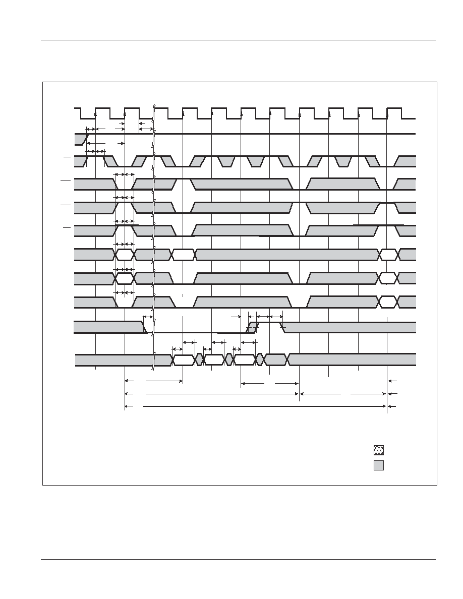
IS42VS16100D
ISSI
Æ
Integrated Silicon Solution, Inc. -- www.issi.com --
1-800-379-4774
57
Rev. 00D
06/30/05
Write Cycle / Precharge Termination
CLK
CKE
CS
RAS
CAS
WE
A0-A9
A10
A11
DQM
DQ
T0
T1
T4
T5
T6
T7
T8
T9
T10
T11
t
CK
t
CHI
t
CL
t
CH
t
CS
t
CH
t
CS
t
CH
t
CS
t
CH
t
CS
t
AH
t
AS
NO PRE
t
AH
t
AS
t
AH
t
AS
t
CKS
t
CKA
BANK 0
BANK 0
BANK 1
BANK 0
BANK 0
BANK 0 OR 1
ROW
ROW
ROW
COLUMN m
ROW
t
RAS
t
RC
t
RC
<
ACT 0
>
<
ACT
>
<
WRIT 0
>
<
PRE 0
>
t
RCD
t
DPL
t
RCD
t
RAS
t
RP
D
IN
0m
D
IN
0m+1
D
IN
0m+2
t
DS
t
DS
t
DS
t
DH
t
DH
t
DH
t
CS
t
CH
t
CS
t
CH
(1)
Don't Care
Undefined
CAS
latency = 2, burst length = 4
Note 1: A8,A9 = Don't Care
.
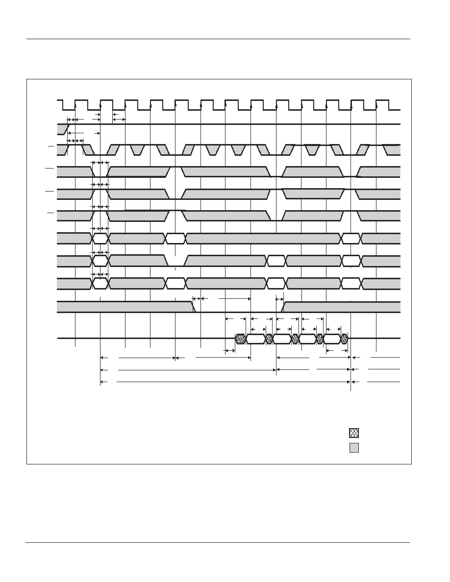
IS42VS16100D
ISSI
Æ
58
Integrated Silicon Solution, Inc. -- www.issi.com --
1-800-379-4774
Rev. 00D
06/30/05
Read Cycle
CLK
CKE
CS
RAS
CAS
WE
A0-A9
A10
A11
DQM
DQ
T0
T1
T2
T3
T4
T5
T6
T7
T8
T9
T10
T11
T12
t
CK
t
CHI
t
CL
t
CH
t
CS
t
CH
t
CS
t
CH
t
CS
t
CH
t
CS
t
AH
t
AS
BANK 1
BANK 0 AND 1
BANK 0 OR 1
NO PRE
t
AH
t
AS
t
CS
t
AH
t
AS
t
CKS
t
CKA
BANK 0
BANK 0
BANK 1
BANK 1
BANK 0
BANK 1
BANK 0
ROW
COLUMN m
ROW
t
QMD
t
LZ
t
RAS
t
RC
<
ACT
>
<
READ
>
<
ACT
>
<
PRE
>
<
PALL
>
t
RCD
t
CAC
t
RQL
t
RP
t
RCD
t
AC
t
AC
t
OH
t
AC
t
AC
t
OH
t
CH
t
OH
D
OUT
m
D
OUT
m+1
D
OUT
m+2
t
OH
t
HZ
D
OUT
m+3
t
RC
t
RAS
(1)
ROW
ROW
Don't Care
Undefined
CAS
latency = 3, burst length = 4
Note 1: A8,A9 = Don't Care
.
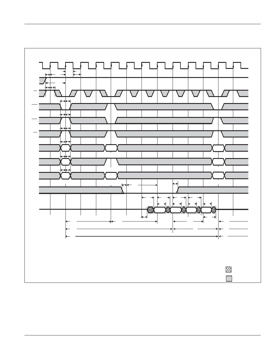
IS42VS16100D
ISSI
Æ
Integrated Silicon Solution, Inc. -- www.issi.com --
1-800-379-4774
59
Rev. 00D
06/30/05
Read Cycle / Auto-Precharge
CLK
CKE
CS
RAS
CAS
WE
A0-A9
A10
A11
DQM
DQ
T0
T1
T2
T3
T4
T5
T6
T7
T8
T9
T10
T11
T12
t
CK
t
CHI
t
CL
t
CH
t
CS
t
CH
t
CS
t
CH
t
CS
t
CH
t
CS
t
AH
t
AS
BANK 1
AUTO PRE
t
AH
t
AS
t
CS
t
AH
t
AS
t
CKS
t
CKA
BANK 0
BANK 0
BANK 1
ROW
ROW
ROW
COLUMN
ROW
t
QMD
t
LZ
t
RAS
t
RC
<
ACT
>
<
READA
>
<
ACT
>
t
RCD
t
CAC
t
PQL
t
RP
t
RCD
t
AC
t
AC
t
OH
t
AC
t
AC
t
OH
t
CH
t
OH
D
OUT
m
D
OUT
m+1
D
OUT
m+2
t
OH
t
HZ
D
OUT
m+3
t
RC
t
RAS
(1)
BANK 1
BANK 0
CAS
latency = 3, burst length = 4
Don't Care
Undefined
Note 1: A8,A9 = Don't Care
.
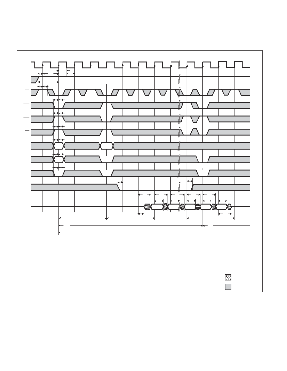
IS42VS16100D
ISSI
Æ
60
Integrated Silicon Solution, Inc. -- www.issi.com --
1-800-379-4774
Rev. 00D
06/30/05
Read Cycle / Full Page
CLK
CKE
CS
RAS
CAS
WE
A0-A9
A10
A11
DQM
DQ
T0
T1
T2
T3
T4
T5
T6
T7
T8
T262
T263
T264
T265
t
CK
t
CHI
t
CL
t
CH
t
CS
t
CH
t
CS
t
CH
t
CS
t
CH
t
CS
t
AH
t
AS
NO PRE
t
AH
t
AS
t
CS
t
AH
t
AS
t
CKS
t
CKA
BANK 0
BANK 0
BANK 0 OR 1
BANK 0
ROW
COLUMN
ROW
t
LZ
t
RAS
(BANK 0)
t
RC
(BANK 0)
<
ACT 0
>
<
READ0
>
<
BST
>
<
PRE 0
>
t
RCD
(BANK 0)
t
CAC
(BANK 0)
t
RBD
t
AC
t
AC
t
OH
t
AC
t
AC
t
AC
t
OH
t
CH
t
OH
D
OUT
0m
D
OUT
0m+1
D
OUT
0m-1
t
OH
t
HZ
t
OH
D
OUT
0m
D
OUT
0m+1
t
RP
(BANK 0)
(1)
CAS
latency = 3, burst length = full page
Don't Care
Undefined
Note 1: A8,A9 = Don't Care
.
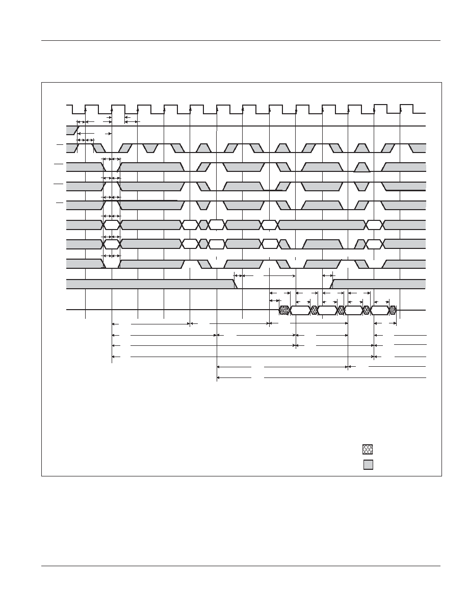
IS42VS16100D
ISSI
Æ
Integrated Silicon Solution, Inc. -- www.issi.com --
1-800-379-4774
61
Rev. 00D
06/30/05
Read Cycle / Ping Pong Operation (Bank Switching)
CLK
CKE
CS
RAS
CAS
WE
A0-A9
A10
A11
DQM
DQ
T0
T1
T2
T3
T4
T5
T6
T7
T8
T9
T10
T11
T12
t
CK
t
CHI
t
CL
t
CH
t
CS
t
CH
t
CS
t
CH
t
CS
t
CH
t
CS
t
AH
t
AS
BANK 0
BANK 1
BANK 0
BANK1
BANK 0
BANK 1
BANK 0
BANK 0 OR 1
BANK 0 OR 1
NO PRE
NO PRE
t
CH
t
AH
t
AS
t
QMD
t
CS
t
AC
t
AC
t
AC
t
AC
t
RCD
(BANK 0)
t
RAS
(BANK 0)
<
ACT 0
>
<
ACT 0
>
<
ACT1
>
<
READ 0
>
<
READA 0
>
<
READA 1
>
<
READ 1
>
<
PRE 0
>
<
PRE 1
>
t
AH
t
AS
t
CKS
t
CKA
ROW
ROW
ROW
ROW
ROW
COLUMN
COLUMN
AUTO PRE
AUTO PRE
ROW
t
LZ
t
RAS
(BANK 1)
t
RC
(BANK 1)
t
RCD
(BANK 1)
t
CAC
(BANK 1)
t
CAC
(BANK 0)
t
RC
(BANK 0)
t
RQL
(BANK 0)
t
RP
(BANK 0)
t
RCD
(BANK 0)
t
RAS
(BANK 0)
t
RP
(BANK1)
t
RC
(BANK 0)
t
RRD
(BANK 0 TO 1)
t
OH
t
OH
t
OH
t
OH
t
HZ
D
OUT
0m
D
OUT
0m+1
D
OUT
1m
D
OUT
1m+1
(1)
(1)
2
2
CAS
latency = 3, burst length = 2
Don't Care
Undefined
Notes:
1. A8,A9 = Don't Care.
2. Depending on the clock cycle time, it may be necessary to delay PRE1 and ACT0 by one cycle to meet t
RAS
(BANK 1).
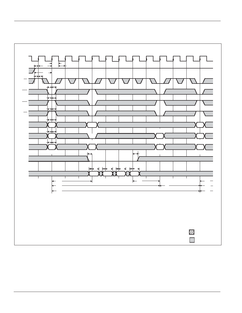
IS42VS16100D
ISSI
Æ
62
Integrated Silicon Solution, Inc. -- www.issi.com --
1-800-379-4774
Rev. 00D
06/30/05
Write Cycle
CLK
CKE
CS
RAS
CAS
WE
A0-A9
A10
A11
DQM
DQ
T0
T1
T2
T3
T4
T5
T7
T6
T8
T9
T10
T11
t
CK
t
CHI
t
CL
t
CH
t
CS
t
CH
t
CS
t
CH
t
CS
t
CH
t
CS
t
AH
t
AS
BANK 1
BANK 0
BANK 0 OR 1
BANK 0 AND 1
NO PRE
t
CH
t
AH
t
AS
t
CS
t
DS
t
DS
t
DS
t
DS
t
DH
t
RAS
t
RC
<
PRE
>
<
PALL
>
<
ACT
>
<
ACT
>
<
WRIT
>
t
AH
t
AS
t
CKS
t
CKA
ROW
ROW
ROW
COLUMN
ROW
t
RCD
t
DH
t
DH
t
DH
t
RP
t
DPL
t
RCD
t
RAS
t
RC
D
IN
m
D
IN
m+2
D
IN
m+1
D
IN
m+3
BANK 1
BANK 0
BANK 1
BANK 0
BANK 1
BANK 0
T12
(1)
CAS
latency = 3, burst length = 4
Don't Care
Undefined
Note 1: A8,A9 = Don't Care
.
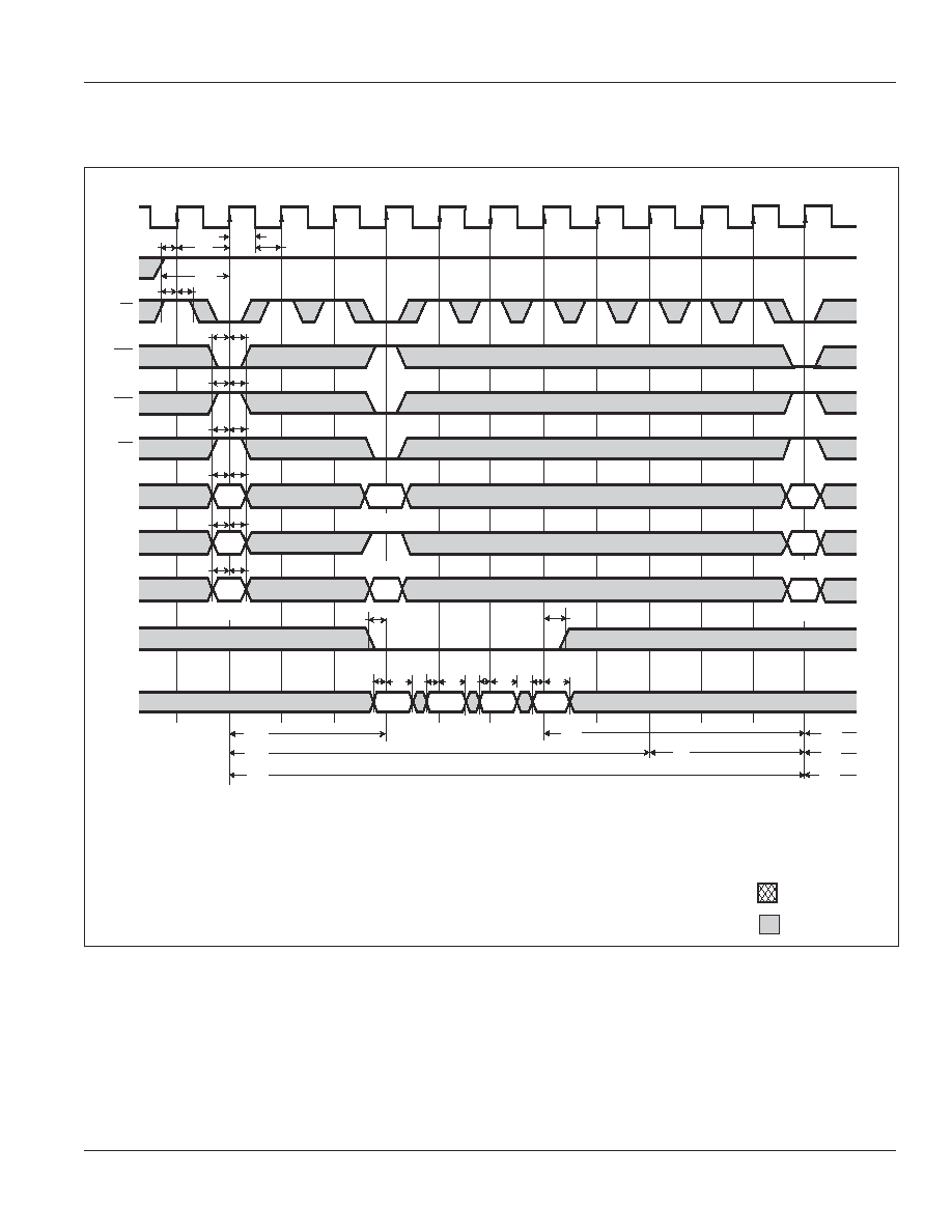
IS42VS16100D
ISSI
Æ
Integrated Silicon Solution, Inc. -- www.issi.com --
1-800-379-4774
63
Rev. 00D
06/30/05
Write Cycle / Auto-Precharge
CLK
CKE
CS
RAS
CAS
WE
A0-A9
A10
A11
DQM
DQ
T0
T1
T2
T3
T4
T5
T7
T6
T8
T9
T10
t
CK
t
CHI
t
CL
t
CH
t
CS
t
CH
t
CS
t
CH
t
CS
t
CH
t
CS
t
AH
t
AS
BANK 1
BANK 0
AUTO PRE
t
CH
t
AH
t
AS
t
CS
t
DS
t
DS
t
DS
t
DS
t
DH
t
RAS
t
RC
<
ACT
>
<
ACT
>
<
WRITA
>
t
AH
t
AS
t
CKS
t
CKA
ROW
ROW
ROW
COLUMN
ROW
t
RCD
t
DH
t
DH
t
DH
t
RP
t
DAL
t
RCD
t
RAS
t
RC
D
IN
m
D
IN
m+2
D
IN
m+1
D
IN
m+3
BANK 1
BANK 0
BANK 1
BANK 0
T11
T12
(1)
CAS
latency = 3, burst length = 4
Don't Care
Undefined
Note 1: A8,A9 = Don't Care
.
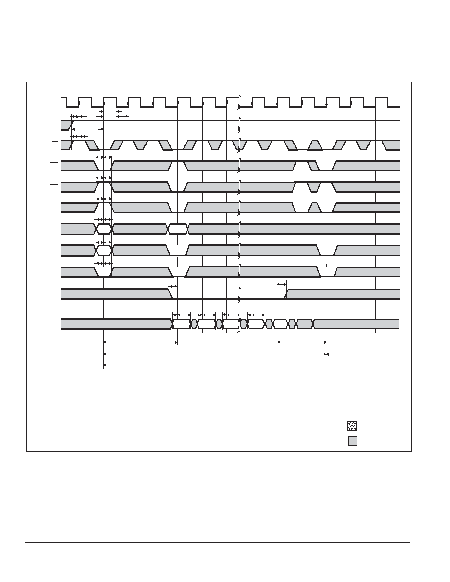
IS42VS16100D
ISSI
Æ
64
Integrated Silicon Solution, Inc. -- www.issi.com --
1-800-379-4774
Rev. 00D
06/30/05
Write Cycle / Full Page
CLK
CKE
CS
RAS
CAS
WE
A0-A9
A10
A11
DQM
DQ
T0
T1
T2
T3
T4
T5
T259
T6
T260
T261
T262
T263
T264
t
CK
t
CHI
t
CL
t
CH
t
CS
t
CH
t
CS
t
CH
t
CS
t
CH
t
CS
t
AH
t
AS
NO PRE
t
AH
t
AS
t
CS
t
AH
t
AS
t
CKS
t
CKA
BANK 0
BANK 0
BANK 0 OR 1
BANK 0
ROW
COLUMN
ROW
t
RAS
t
RC
<
ACT 0
>
<
WRIT0
>
<
BST
>
<
PRE 0
>
t
RCD
t
CH
t
DPL
t
RP
t
DS
t
DS
t
DS
t
DS
t
DH
t
DH
t
DH
t
DH
D
IN
0m
D
IN
0m+2
D
IN
0m+1
D
IN
0m-1
D
IN
0m
(1)
CAS
latency = 3, burst length = full page
Don't Care
Undefined
Note 1: A8,A9 = Don't Care
.
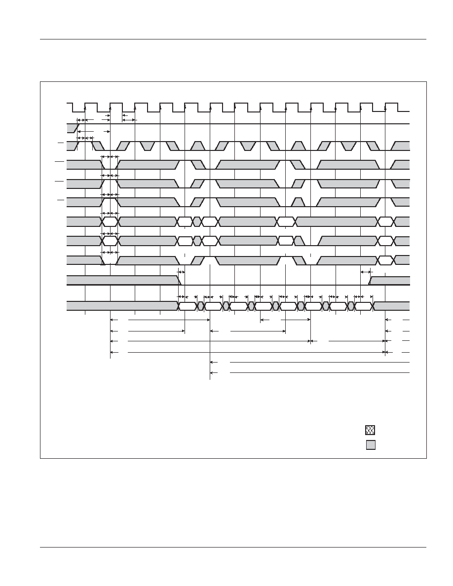
IS42VS16100D
ISSI
Æ
Integrated Silicon Solution, Inc. -- www.issi.com --
1-800-379-4774
65
Rev. 00D
06/30/05
Write Cycle / Ping-Pong Operation (Bank Switching)
CLK
CKE
CS
RAS
CAS
WE
A0-A9
A10
A11
DQM
DQ
T0
T1
T2
T3
T4
T5
T6
T7
T8
T9
T10
t
CK
t
CHI
t
CL
t
CH
t
CS
t
CH
t
CS
t
CH
t
CS
t
CH
t
CS
t
AH
t
AS
BANK 0
BANK 0
BANK 0
BANK 1
BANK 1
BANK 0 OR 1
NO PRE
NO PRE
t
CH
t
AH
t
AS
t
CS
t
DS
t
DS
t
RCD
(BANK 0)
t
RAS
(BANK 0)
<
ACT 0
>
<
ACT 1
>
<
WRIT 0
>
<
WRITA 0
>
<
WRITA 1
>
<
WRIT 1
>
<
PRE 0
>
<
ACT 0
>
t
AH
t
AS
t
CKS
t
CKA
ROW
ROW
ROW
ROW
ROW
COLUMN
COLUMN
AUTO PRE
AUTO PRE
ROW
t
RCD
(BANK 1)
t
RAS
(BANK 1)
t
RC
(BANK 1)
t
RC
(BANK 0)
t
RCD
t
RP
(BANK 0)
t
RAS
t
RC
t
RRD
(BANK 0 TO 1)
t
DPL
(BANK 0)
t
DPL
t
DH
t
DH
t
DS
t
DH
t
DH
D
IN
0m
t
DS
t
DS
t
DH
t
DS
t
DH
t
DH
t
DH
t
DS
t
DS
D
IN
0m+1
D
IN
0m+2
D
IN
0m+3
D
IN
1m
D
IN
1m+1
D
IN
1m+2
D
IN
1m+3
T11
T12
BANK 0
BANK 1
(1)
(1)
CAS
latency = 3, burst length = 4
Don't Care
Undefined
Note 1: A8,A9 = Don't Care
.
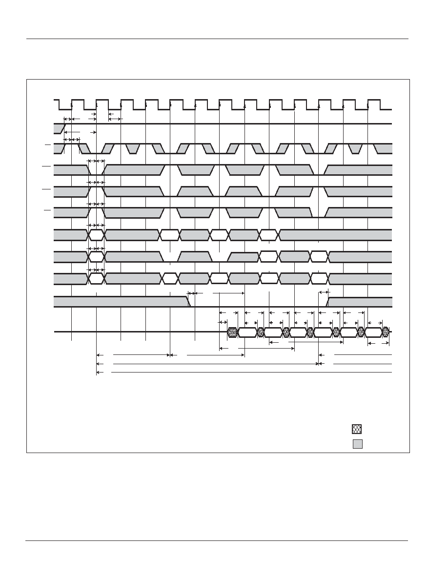
IS42VS16100D
ISSI
Æ
66
Integrated Silicon Solution, Inc. -- www.issi.com --
1-800-379-4774
Rev. 00D
06/30/05
Read Cycle / Page Mode
CLK
CKE
CS
RAS
CAS
WE
A0-A9
A10
A11
DQM
DQ
T0
T1
T2
T3
T4
T5
T6
T7
T8
T9
T10
t
CK
t
CHI
t
CL
t
CH
t
CS
t
CH
t
CS
t
CH
t
CS
t
CH
t
CS
t
AH
t
AS
BANK 1
BANK 0
BANK 0
BANK 0
BANK 0
BANK 1
BANK 0 OR 1
BANK 0 AND 1
BANK 1
t
CH
t
AH
t
AS
t
LZ
t
CS
t
RAS
t
RC
<
ACT
>
<
READ
>
<
READA
>
<
READ
>
<
READ
>
<
PALL
>
<
PRE
>
t
AH
t
AS
t
CKS
t
CKA
ROW
COLUMN m
COLUMN n
COLUMN o
NO PRE
NO PRE
NO PRE
AUTO PRE
ROW
t
RCD
t
CAC
t
CAC
t
CAC
t
RQL
t
HZ
t
RP
t
QMD
BANK 1
BANK 0
BANK 1
t
AC
t
AC
t
OH
t
AC
t
AC
t
AC
t
AC
t
OH
t
OH
t
OH
t
OH
t
OH
D
OUT
m
D
OUT
m+1
D
OUT
n
D
OUT
n+1
D
OUT
o
D
OUT
o+1
T11
T12
(1)
(1)
(1)
CAS
latency = 3, burst length = 2
Don't Care
Undefined
Note 1: A8,A9 = Don't Care
.
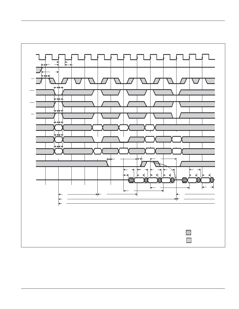
IS42VS16100D
ISSI
Æ
Integrated Silicon Solution, Inc. -- www.issi.com --
1-800-379-4774
67
Rev. 00D
06/30/05
Read Cycle / Page Mode; Data Masking
CAS
latency = 3, burst length = 2
CLK
CKE
CS
RAS
CAS
WE
A0-A9
A10
A11
DQM
DQ
T0
T1
T2
T3
T4
T5
T6
T7
T8
T9
T10
t
CK
t
CHI
t
CL
t
CH
t
CS
t
CH
t
CS
t
CH
t
CS
t
CH
t
CS
t
AH
t
AS
BANK 1
BANK 0
BANK 0
BANK 0
BANK 0
BANK 1
BANK 0 OR 1
BANK 0 AND 1
BANK 1
t
QMD
t
AH
t
AS
t
LZ
t
CS
t
RAS
t
RC
<
ACT
>
<
READ
>
<
READ
>
<
ENB
>
<
READA, MASK
>
<
READ, MASK
>
<
PALL
>
<
PRE
>
t
AH
t
AS
t
CKS
t
CKA
ROW
COLUMN m
COLUMN n
COLUMN o
NO PRE
NO PRE
NO PRE
AUTO PRE
ROW
t
CH
t
RCD
t
CAC
t
CAC
t
CAC
t
RQL
t
HZ
t
RP
t
QMD
BANK 1
BANK 0
BANK 1
t
AC
t
AC
t
OH
t
AC
t
AC
t
AC
t
OH
t
OH
t
OH
t
OH
D
OUT
m
D
OUT
m+1
D
OUT
n
D
OUT
o
D
OUT
o+1
T11
T12
(1)
(1)
(1)
Don't Care
Undefined
Note 1: A8,A9 = Don't Care
.
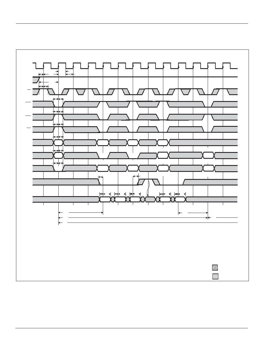
IS42VS16100D
ISSI
Æ
68
Integrated Silicon Solution, Inc. -- www.issi.com --
1-800-379-4774
Rev. 00D
06/30/05
Write Cycle / Page Mode; Data Masking
CAS
latency = 3, burst length = 2
CLK
CKE
CS
RAS
CAS
WE
A0-A9
A10
A11
DQM
DQ
T0
T1
T2
T3
T4
T5
T6
T7
T8
T9
T10
t
CK
t
CHI
t
CL
t
CH
t
CS
t
CH
t
CS
t
CH
t
CS
t
CH
t
CS
t
AH
t
AS
BANK 0
BANK 0
BANK 0
BANK 0
BANK 1
BANK 0 OR 1
BANK 0 AND 1
BANK 1
t
CH
t
AH
t
AS
t
CS
t
RAS
t
RC
<
ACT
>
<
WRIT
>
<
WRITA
>
<
WRIT
>
<
WRIT
>
<
MASK
>
<
PALL
>
<
PRE
>
t
AH
t
AS
t
CKS
t
CKA
ROW
COLUMN m
COLUMN n
COLUMN o
NO PRE
NO PRE
NO PRE
AUTO PRE
ROW
t
RCD
t
DPL
t
RP
BANK 1
BANK 0
BANK 1
t
DS
t
DS
t
DS
t
DH
t
DS
t
DH
t
DH
t
DH
t
DS
t
DH
D
IN
m
D
IN n
D
IN
m+1
D
IN
o
D
IN
o+1
T11
T12
(1)
(1)
(1)
Don't Care
Undefined
Note 1: A8,A9 = Don't Care
.
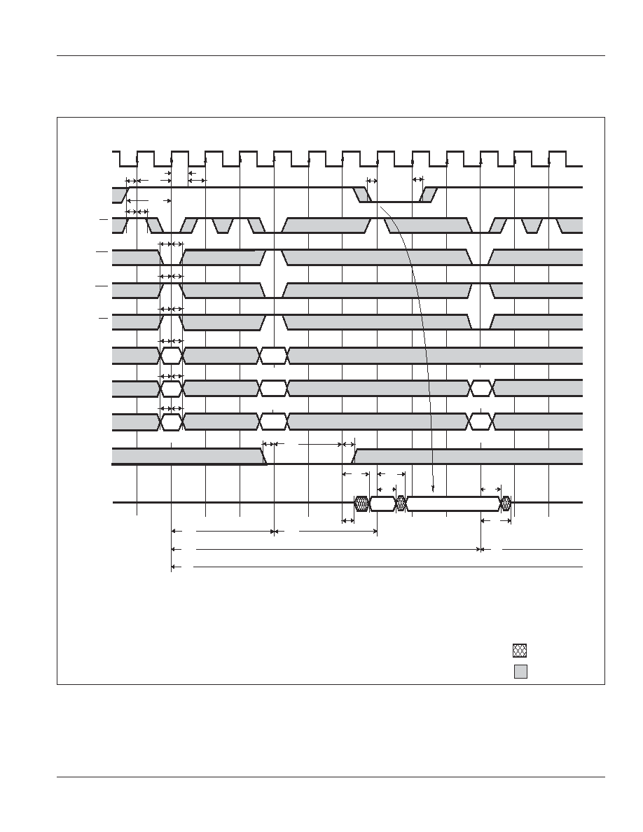
IS42VS16100D
ISSI
Æ
Integrated Silicon Solution, Inc. -- www.issi.com --
1-800-379-4774
69
Rev. 00D
06/30/05
Read Cycle / Clock Suspend
CAS
latency = 3, burst length = 2
CLK
CKE
CS
RAS
CAS
WE
A0-A9
A10
A11
DQM
DQ
T0
T1
T2
T3
T4
T5
T6
T7
T8
T9
T10
T11
t
CK
t
CHI
t
CL
t
CH
t
CS
t
CH
t
CS
t
CH
t
CS
t
CH
t
CS
t
AH
t
AS
NO PRE
AUTO PRE
t
AH
t
AS
t
CS
t
CKH
t
AH
t
AS
t
CKS
t
CKA
t
CKS
BANK 1
BANK 0
BANK 0
BANK 1
BANK 0
BANK 0 AND 1
BANK 0 OR 1
ROW
COLUMN m
ROW
t
QMD
t
LZ
t
RAS
t
RC
<
ACT
>
<
READ
>
<
READ A
>
<
SPND
>
<
SPND
>
<
PRE
>
<
PALL
>
t
RCD
t
CAC
t
AC
t
AC
t
OH
t
OH
t
CH
D
OUT
m
D
OUT
m+1
t
HZ
t
RP
T12
BANK 1
(1)
Don't Care
Undefined
Note 1: A8,A9 = Don't Care
.
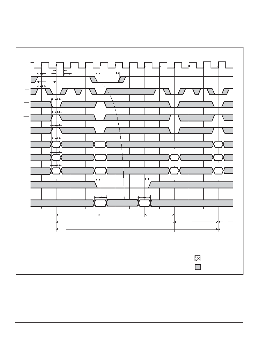
IS42VS16100D
ISSI
Æ
70
Integrated Silicon Solution, Inc. -- www.issi.com --
1-800-379-4774
Rev. 00D
06/30/05
Write Cycle / Clock Suspend
CAS
latency = 3, burst length = 2
CLK
CKE
CS
RAS
CAS
WE
A0-A9
A10
A11
DQM
DQ
T0
T1
T2
T3
T4
T5
T6
T7
T8
T9
T10
t
CK
t
CHI
t
CL
t
CH
t
CS
t
CH
t
CS
t
CH
t
CS
t
CH
t
CS
t
AH
t
AS
NO PRE
AUTO PRE
t
AH
t
AS
t
CS
t
CKH
t
AH
t
AS
t
CKS
t
CKA
t
CKS
BANK 1
BANK 0
BANK 1
BANK 1
BANK 0
BANK 0
BANK 1
BANK 0
BANK 0 AND 1
BANK 0 OR 1
ROW
ROW
ROW
COLUMN m
ROW
t
DS
t
RAS
t
RC
t
RC
<
ACT
>
<
ACT
>
<
WRIT, SPND
>
<
WRITA, SPND
>
<
SPND
>
<
PRE
>
<
PALL
>
t
RCD
t
CH
t
DH
t
DH
t
DS
t
DPL
t
RP
t
RAS
D
IN
m
D
IN
m+1
T11
T12
(1)
Don't Care
Undefined
Note 1: A8,A9 = Don't Care
.
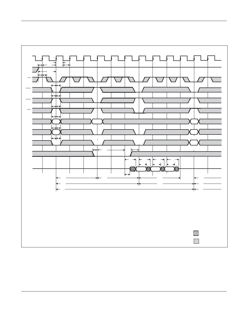
IS42VS16100D
ISSI
Æ
Integrated Silicon Solution, Inc. -- www.issi.com --
1-800-379-4774
71
Rev. 00D
06/30/05
Read Cycle / Precharge Termination
CAS
latency = 3, burst length = 4
CLK
CKE
CS
RAS
CAS
WE
A0-A9
A10
A11
DQM
DQ
T0
T1
T2
T3
T4
T5
T6
T7
T8
T9
T10
t
CK
t
CHI
t
CL
t
CH
t
CS
t
CH
t
CS
t
CH
t
CS
t
CH
t
CS
t
AH
t
AS
NO PRE
t
AH
t
AS
t
CS
t
AH
t
AS
t
CKS
t
CKA
BANK 0
BANK 0
BANK 0
ROW
ROW
ROW
COLUMN m
ROW
t
QMD
t
LZ
t
RAS
t
RC
t
RP
<
ACT 0
>
<
ACT
>
<
READ 0
>
<
PRE 0
>
t
RCD
t
CAC
t
RQL
t
RP
t
RCD
t
AC
t
AC
t
OH
t
AC
t
HZ
t
OH
t
OH
t
CH
D
OUT
m
D
OUT
m+2
t
RAS
BANK 1
D
OUT
m+1
T11
T12
BANK 0
BANK 0 OR 1
(1)
Don't Care
Undefined
Note 1: A8,A9 = Don't Care
.
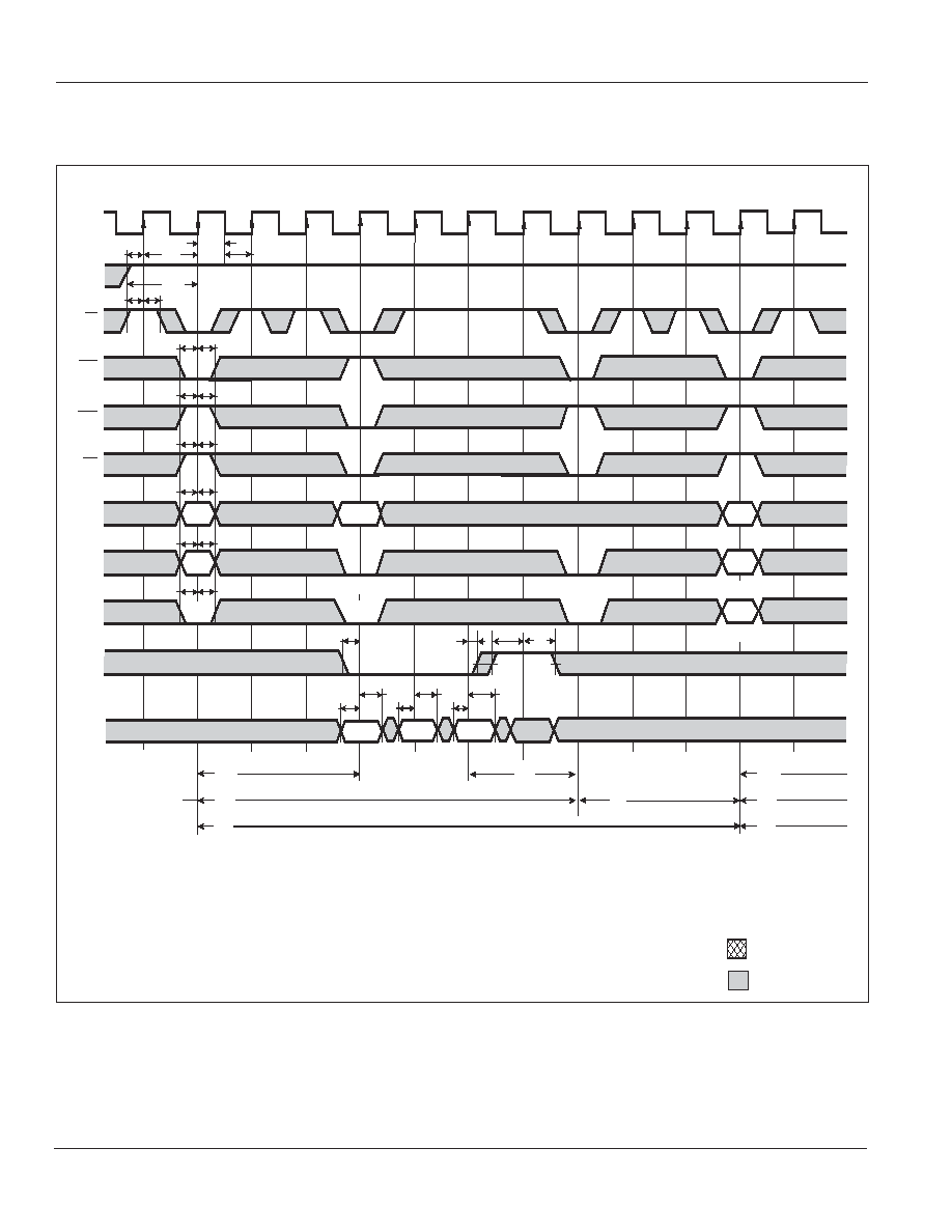
IS42VS16100D
ISSI
Æ
72
Integrated Silicon Solution, Inc. -- www.issi.com --
1-800-379-4774
Rev. 00D
06/30/05
Write Cycle / Precharge Termination
CAS
latency = 3, burst length = 4
CLK
CKE
CS
RAS
CAS
WE
A0-A9
A10
A11
DQM
DQ
T0
T1
T2
T3
T4
T5
T6
T7
T8
T9
T10
t
CK
t
CHI
t
CL
t
CH
t
CS
t
CH
t
CS
t
CH
t
CS
t
CH
t
CS
t
AH
t
AS
NO PRE
t
AH
t
AS
t
AH
t
AS
t
CKS
t
CKA
BANK 0
BANK 0
BANK 0
ROW
ROW
ROW
COLUMN m
ROW
t
RC
t
RP
<
ACT 0
>
<
ACT
>
<
WRIT 0
>
<
PRE 0
>
t
RCD
t
RP
t
RCD
t
RAS
BANK 1
D
IN
0m
D
IN
0m+1
D
IN
0m+2
t
DS
t
DS
t
DS
t
DH
t
DH
t
DH
T11
T12
t
CH
t
CH
t
CS
t
CS
BANK 0
BANK 0 OR 1
t
RAS
(1)
t
DPL
Don't Care
Undefined
Note 1: A8,A9 = Don't Care
.

IS42VS16100D
ISSI
Æ
Integrated Silicon Solution, Inc. -- www.issi.com --
1-800-379-4774
73
Rev. 00D
06/30/05
ORDERING INFORMATION
Commercial Range: 0
∞∞
∞∞
∞
C to +70
∞∞
∞∞
∞
C
(1.7V-1.9V)
Frequency
Speed (ns)
Order Part No.
Package
135 MHz
7.4
IS42VS16100D-75T
50-pin, TSOP-II
135 MHz
7.4
IS42VS16100D-75TL
50-pin, TSOP-II, Lead-free
100 MHz
10
IS42VS16100D-10T
50-pin, TSOP-II
100 MHz
10
IS42VS16100D-10TL
50-pin, TSOP-II, Lead-free
Extended Range: -25
∞∞
∞∞
∞
C to +85
∞∞
∞∞
∞
C
(1.7V-1.9V)
Frequency
Speed (ns)
Order Part No.
Package
135 MHz
7.4
IS42VS16100D-75TE
50-pin, TSOP-II
135 MHz
7.4
IS42VS16100D-75TLE
50-pin, TSOP-II, Lead-free
100 MHz
10
IS42VS16100D-10TE
50-pin, TSOP-II
100 MHz
10
IS42VS16100D-10TLE
50-pin, TSOP-II, Lead-free
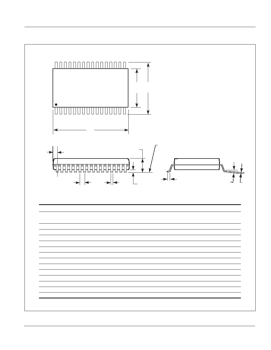
PACKAGING INFORMATION
ISSI
Æ
Integrated Silicon Solution, Inc. -- www.issi.com --
1-800-379-4774
Rev. F
06/18/03
Copyright © 2003 Integrated Silicon Solution, Inc. All rights reserved. ISSI reserves the right to make changes to this specification and its products at any time
without notice. ISSI assumes no liability arising out of the application or use of any information, products or services described herein. Customers are advised to
obtain the latest version of this device specification before relying on any published information and before placing orders for products.
Plastic TSOP
Package Code: T (Type II)
D
SEATING PLANE
b
e
C
1
N/2
N/2+1
N
E1
A1
A
E
L
ZD
.
Notes:
1. Controlling dimension: millimieters,
unless otherwise specified.
2. BSC = Basic lead spacing
between centers.
3. Dimensions D and E1 do not
include mold flash protrusions and
should be measured from the
bottom of the package.
4. Formed leads shall be planar with
respect to one another within
0.004 inches at the seating plane.
Plastic TSOP (T - Type II)
Millimeters
Inches
Millimeters
Inches
Millimeters
Inches
Symbol Min
Max
Min
Max
Min
Max
Min
Max
Min
Max
Min
Max
Ref. Std.
No. Leads (N)
32
44
50
A
--
1.20
--
0.047
--
1.20
--
0.047
--
1.20
--
0.047
A1
0.05
0.15
0.002 0.006
0.05
0.15
0.002 0.006
0.05
0.15
0.002 0.006
b
0.30
0.52
0.012 0.020
0.30
0.45
0.012 0.018
0.30
0.45
0.012 0.018
C
0.12
0.21
0.005 0.008
0.12
0.21
0.005 0.008
0.12
0.21
0.005 0.008
D
20.82 21.08
0.820 0.830
18.31 18.52
0.721 0.729
20.82 21.08
0.820 0.830
E1
10.03 10.29
0.391 0.400
10.03 10.29
0.395 0.405
10.03 10.29
0.395 0.405
E
11.56 11.96
0.451 0.466
11.56 11.96
0.455 0.471
11.56 11.96
0.455 0.471
e
1.27 BSC
0.050 BSC
0.80 BSC
0.032 BSC
0.80 BSC
0.031 BSC
L
0.40
0.60
0.016 0.024
0.41
0.60
0.016 0.024
0.40
0.60
0.016 0.024
ZD 0.95 REF 0.037 REF 0.81 REF 0.032 REF 0.88 REF 0.035 REF
0∞
5∞
0∞
5∞
0∞
5∞
0∞
5∞
0∞
5∞
0∞
5∞