
Integrated Silicon Solution, Inc. -- www.issi.com --
1-800-379-4774
1
Rev. A
10/06/02
IS61LF25632T/D/J
IS61LF25636T/D/J
IS61LF51218T/D/J
ISSI
Æ
Copyright © 2002 Integrated Silicon Solution, Inc. All rights reserved. ISSI reserves the right to make changes to this specification and its products at any time
without notice. ISSI assumes no liability arising out of the application or use of any information, products or services described herein. Customers are advised to
obtain the latest version of this device specification before relying on any published information and before placing orders for products.
FEATURES
∑ Internal self-timed write cycle
∑ Individual Byte Write Control and Global
Write
∑ Clock controlled, registered address, data
and control
∑ Interleaved or linear burst sequence control
using MODE input
∑ Three chip enable option for simple depth
expansion and address pipelining
∑ Common data inputs and data outputs
∑ JEDEC 100-Pin TQFP and
119-pin PBGA package
∑ Power Supply
+ 3.3V V
DD
+ 3.3V or 2.5V V
DDQ
(I/0)
∑ Snooze MODE for reduced-power standby
∑ T version (three chip selects)
∑ J version (PBGA Package with JTAG)
∑ D version (two chip selects)
∑ JTAG Boundary Scan for PBGA.
256K x 32, 256K x 36, 512K x 18
SYNCHRONOUS FLOW-THROUGH
STATIC RAM
OCTOBER 2002
FAST ACCESS TIME
Symbol
Parameter
6.5
7.5
Units
t
KQ
Clock Access Time
6.5
7.5
ns
t
KC
Cycle Time
7.5
8.5
ns
Frequency
133
117
MHz
DESCRIPTION
The
ISSI
IS61LF25632, IS61LF25636, and IS61LF51218 are
high-speed, low-power synchronous static RAMs designed to
provide a burstable, high-performance and memories for
commucation and networking applications. The IS61LF25632
is organized as 262,144 words by 32 bits and the IS61LF25636
is organized as 262,144 words by 36 bits. The IS61LF51218 is
organized as 524,288 words by 18 bits. Fabricated with
ISSI
's
advanced CMOS technology, the device integrates a 2-bit
burst counter, high-speed SRAM core, and high-drive capability
outputs into a single monolithic circuit. All synchronous inputs
pass through registers that are controlled by a positive-edge-
triggered single clock input.
Write cycles are internally self-timed and are initiated by the rising
edge of the clock input. Write cycles can be from one to four bytes
wide as controlled by the write control inputs.
Separate byte enables allow individual bytes to be written. Byte
write operation is performed by using byte write enable
(
BWE
).input combined with one or more individual byte write
signals (
BWx
). In addition, Global Write (
GW
) is available for
writing all bytes at one time, regardless of the byte write
controls.
Bursts can be initiated with either
ADSP
(Address Status
Processor) or
ADSC
(Address Status Cache Controller) input
pins. Subsequent burst addresses can be generated internally
and controlled by the
ADV
(burst address advance) input pin.
The mode pin is used to select the burst sequence order, Linear
burst is achieved when this pin is tied LOW. Interleave burst is
achieved when this pin is tied HIGH or left floating.
2
Integrated Silicon Solution, Inc. -- www.issi.com --
1-800-379-4774
Rev. A
10/06/02
IS61LF25632T/D/J
IS61LF25636T/D/J
IS61LF51218T/D/J
ISSI
Æ
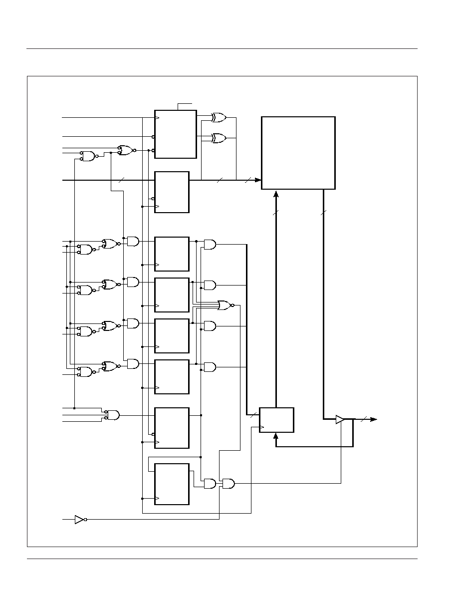
BLOCK DIAGRAM
BINARY
COUNTER
BWa
GW
CLR
CE
CLK
Q0
Q1
MODE
A0'
A0
A1
A1'
CLK
ADV
ADSC
ADSP
16/17
18/19
ADDRESS
REGISTER
CE
D
CLK
Q
DQd
BYTE WRITE
REGISTERS
D
CLK
Q
DQc
BYTE WRITE
REGISTERS
D
CLK
Q
DQb
BYTE WRITE
REGISTERS
D
CLK
Q
DQa
BYTE WRITE
REGISTERS
D
CLK
Q
ENABLE
REGISTER
CE
D
CLK
Q
ENABLE
DELAY
REGISTER
D
CLK
Q
BWE
BWd
CE
(T,D)
CE2
(T)
CE2 (T,D)
BWb
BWc
256K x 32; 256K x 36;
512K x 18
MEMORY ARRAY
INPUT
REGISTERS
CLK
32, 36,
or 18
OE
4
OE
DQa - DQd
18/19
A
(x32/x36)
(x32/x36/x18)
(x32/x36)
(x32/x36/x18)
32, 36,
or 18
32, 36,
or 18
Integrated Silicon Solution, Inc. -- www.issi.com --
1-800-379-4774
3
Rev.A
10/06/02
IS61LF25632T/D/J
IS61LF25636T/D/J
IS61LF51218T/D/J
ISSI
Æ
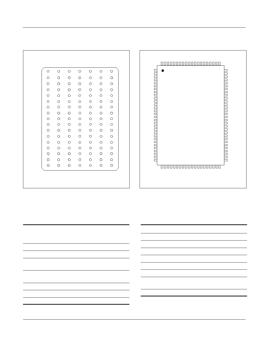
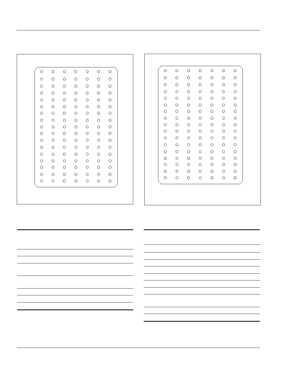
PIN CONFIGURATION
119-pin PBGA (Top View) (D Version)
256K x 32
PIN DESCRIPTIONS
A0, A1
Synchronous Address Inputs. These
pins must tied to the two LSBs of the
address bus.
A
Synchronous Address Inputs
CLK
Synchronous Clock
ADSP
Synchronous Processor Address
Status
ADSC
Synchronous Controller Address
Status
ADV
Synchronous Burst Address Advance
BWa
-
BWd
Synchronous Byte Write Enable
BWE
Synchronous Byte Write Enable
GW
Synchronous Global Write Enable
CE
, CE2
Synchronous Chip Enable
OE
Output Enable
DQa-DQd
Synchronous Data Input/Output
MODE
Burst Sequence Mode Selection
V
DD
+3.3V Power Supply
GND
Ground
V
DDQ
Isolated Output Buffer Supply:
+3.3V or 2.5V
ZZ
Snooze Enable
A
B
C
D
E
F
G
H
J
K
L
M
N
P
R
T
U
V
DDQ
NC
NC
DQc
DQc
V
DDQ
DQc
DQc
V
DDQ
DQd
DQd
V
DDQ
DQd
DQd
NC
NC
V
DDQ
A
CE2
A
NC
DQc
DQc
DQc
DQc
V
DD
DQd
DQd
DQd
DQd
NC
A
NC
NC
A
A
A
GND
GND
GND
BWc
GND
NC
GND
BWd
GND
GND
GND
MODE
A
NC
ADSP
ADSC
V
DD
NC
CE
OE
ADV
GW
V
DD
CLK
NC
BWE
A1
A0
V
DD
A
NC
A
A
A
GND
GND
GND
BWb
GND
NC
GND
BWa
GND
GND
GND
GND
A
NC
A
A
A
NC
DQb
DQb
DQb
DQb
V
DD
DQa
DQa
DQa
DQa
NC
A
NC
NC
V
DDQ
NC
NC
DQb
DQb
V
DDQ
DQb
DQb
V
DDQ
DQa
DQa
V
DDQ
DQa
DQa
NC
ZZ
V
DDQ
1
2
3
4
5
6
7
NC
DQb
DQb
V
DDQ
GND
DQb
DQb
DQb
DQb
GND
V
DDQ
DQb
DQb
GND
NC
V
DD
ZZ
DQa
DQa
V
DDQ
GND
DQa
DQa
DQa
DQa
GND
V
DDQ
DQa
DQa
NC
NC
DQc
DQc
V
DDQ
GND
DQc
DQc
DQc
DQc
GND
V
DDQ
DQc
DQc
NC
V
DD
NC
GND
DQd
DQd
V
DDQ
GND
DQd
DQd
DQd
DQd
GND
V
DDQ
DQd
DQd
NC
1
2
3
4
5
6
7
8
9
10
11
12
13
14
15
16
17
18
19
20
21
22
23
24
25
26
27
28
29
30
80
79
78
77
76
75
74
73
72
71
70
69
68
67
66
65
64
63
62
61
60
59
58
57
56
55
54
53
52
51
100 99 98 97 96 95 94 93 92 91 90 89 88 87 86 85 84 83 82 81
31 32 33 34 35 36 37 38 39 40 41 42 43 44 45
MODE
A
A
A
A
A1
A0
NC
NC
GND
V
DD
NC
NC
A
A
A
A
A
A
A
46 47 48 49 50
A
A
CE
CE2
BWd
BWc
BWb
BWa
A
V
DD
GND
CLK
GW
BWE
OE
ADSC
ADSP
ADV
A
A
256K x 32
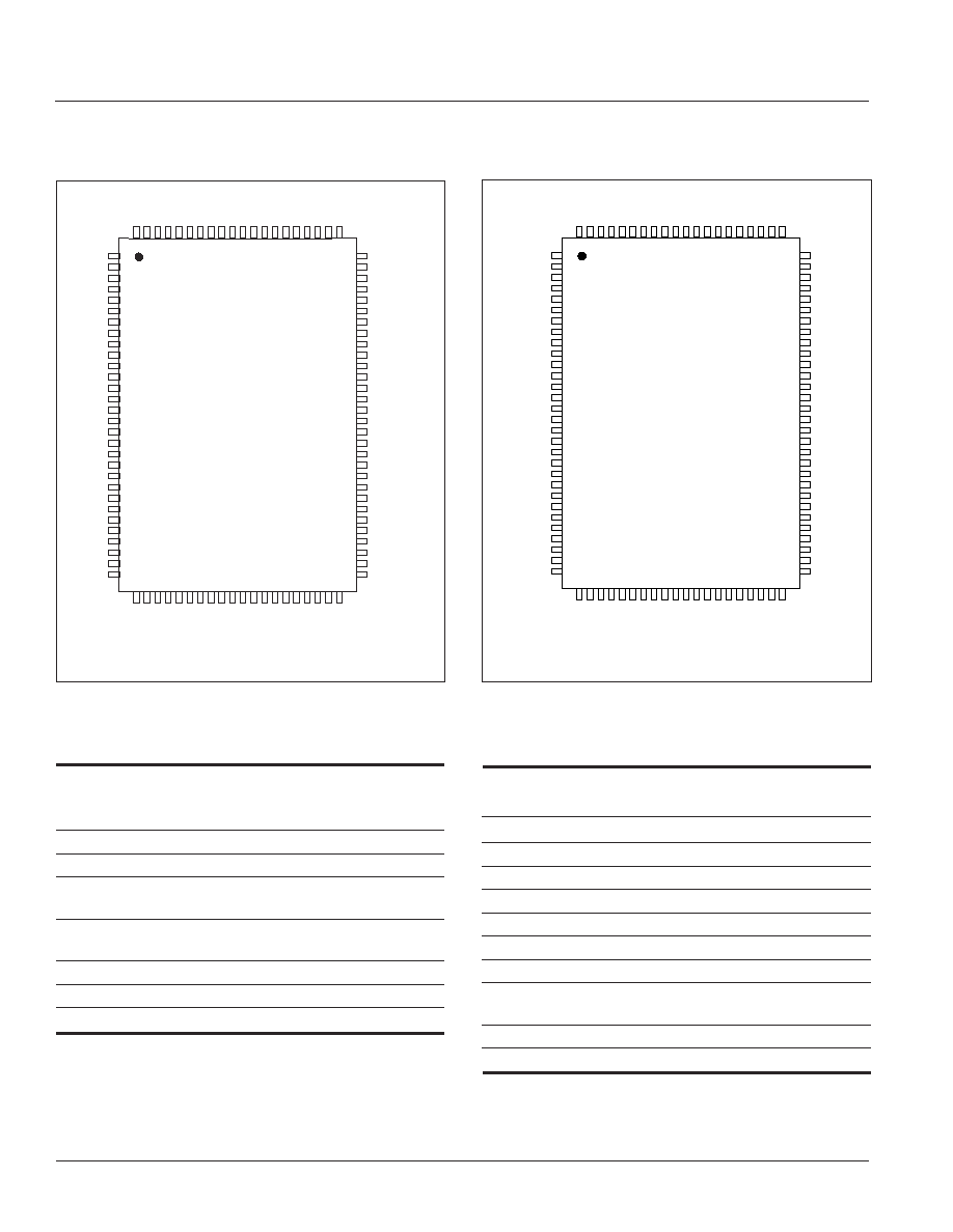
100-Pin TQFP (D Version)
4
Integrated Silicon Solution, Inc. -- www.issi.com --
1-800-379-4774
Rev. A
10/06/02
IS61LF25632T/D/J
IS61LF25636T/D/J
IS61LF51218T/D/J
ISSI
Æ
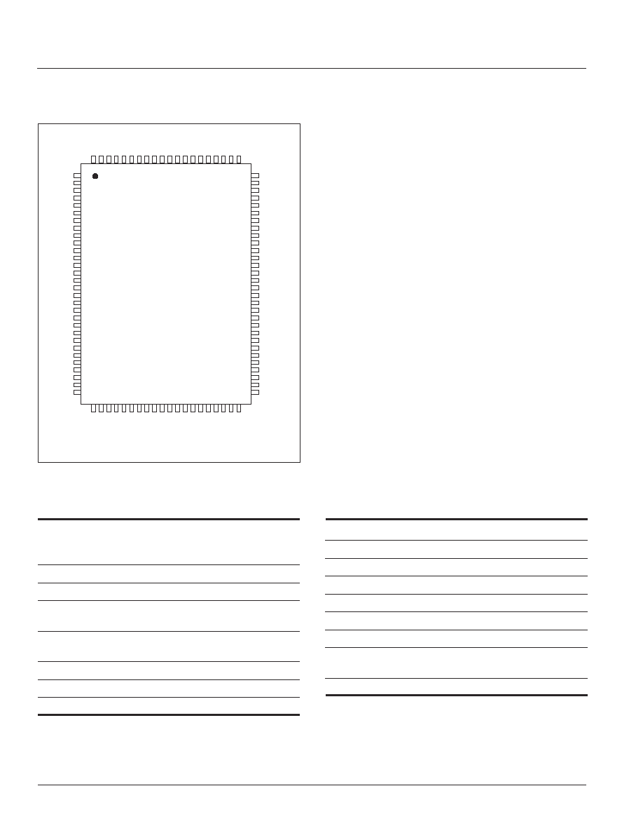
PIN CONFIGURATION
100-Pin TQFP (T Version)
256K x 32
PIN DESCRIPTIONS
A0, A1
Synchronous Address Inputs. These
pins must tied to the two LSBs of the
address bus.
A
Synchronous Address Inputs
CLK
Synchronous Clock
ADSP
Synchronous Processor Address
Status
ADSC
Synchronous Controller Address
Status
ADV
Synchronous Burst Address Advance
BWa
-
BWd
Synchronous Byte Write Enable
BWE
Synchronous Byte Write Enable
GW
Synchronous Global Write Enable
CE
,
CE2
, CE2 Synchronous Chip Enable
OE
Output Enable
DQa-DQd
Synchronous Data Input/Output
MODE
Burst Sequence Mode Selection
V
DD
+3.3V Power Supply
GND
Ground
V
DDQ
Isolated Output Buffer Supply:
+3.3V or 2.5V
ZZ
Snooze Enable
NC
DQb
DQb
V
DDQ
GND
DQb
DQb
DQb
DQb
GND
V
DDQ
DQb
DQb
GND
NC
V
DD
ZZ
DQa
DQa
V
DDQ
GND
DQa
DQa
DQa
DQa
GND
V
DDQ
DQa
DQa
NC
NC
DQc
DQc
V
DDQ
GND
DQc
DQc
DQc
DQc
GND
V
DDQ
DQc
DQc
NC
V
DD
NC
GND
DQd
DQd
V
DDQ
GND
DQd
DQd
DQd
DQd
GND
V
DDQ
DQd
DQd
NC
1
2
3
4
5
6
7
8
9
10
11
12
13
14
15
16
17
18
19
20
21
22
23
24
25
26
27
28
29
30
80
79
78
77
76
75
74
73
72
71
70
69
68
67
66
65
64
63
62
61
60
59
58
57
56
55
54
53
52
51
100 99 98 97 96 95 94 93 92 91 90 89 88 87 86 85 84 83 82 81
31 32 33 34 35 36 37 38 39 40 41 42 43 44 45
MODE
A
A
A
A
A1
A0
NC
NC
GND
V
DD
NC
A
A
A
A
A
A
A
A
46 47 48 49 50
A
A
CE
CE2
BWd
BWc
BWb
BWa
CE2
V
DD
GND
CLK
GW
BWE
OE
ADSC
ADSP
ADV
A
A
Integrated Silicon Solution, Inc. -- www.issi.com --
1-800-379-4774
5
Rev.A
10/06/02
IS61LF25632T/D/J
IS61LF25636T/D/J
IS61LF51218T/D/J
ISSI
Æ
PIN DESCRIPTIONS
A0, A1
Synchronous Address Inputs. These
pins must tied to the two LSBs of the
address bus.
A
Synchronous Address Inputs
CLK
Synchronous Clock
ADSP
Synchronous Processor Address
Status
ADSC
Synchronous Controller Address
Status
ADV
Synchronous Burst Address Advance
BWa
-
BWd
Individual Byte Write Enable
BWE
Synchronous Byte Write Enable
TMS, TDI
JTAG Boundry Scan Pins
TCK, TDO
GW
Synchronous Global Write Enable
CE
, CE2
Synchronous Chip Enable
OE
Output Enable
DQa-DQd
Synchronous Data Input/Output
MODE
Burst Sequence Mode Selection
V
DD
+3.3V Power Supply
GND
Ground
V
DDQ
Isolated Output Buffer Supply:
+3.3V or 2.5V
ZZ
Snooze Enable
DQPa-DQPd
Parity Data I/O
256K x 36
100-Pin TQFP (D Version)
DQPb
DQb
DQb
V
DDQ
GND
DQb
DQb
DQb
DQb
GND
V
DDQ
DQb
DQb
GND
NC
V
DD
ZZ
DQa
DQa
V
DDQ
GND
DQa
DQa
DQa
DQa
GND
V
DDQ
DQa
DQa
DQPa
DQPc
DQc
DQc
V
DDQ
GND
DQc
DQc
DQc
DQc
GND
V
DDQ
DQc
DQc
NC
V
DD
NC
GND
DQd
DQd
V
DDQ
GND
DQd
DQd
DQd
DQd
GND
V
DDQ
DQd
DQd
DQPd
1
2
3
4
5
6
7
8
9
10
11
12
13
14
15
16
17
18
19
20
21
22
23
24
25
26
27
28
29
30
80
79
78
77
76
75
74
73
72
71
70
69
68
67
66
65
64
63
62
61
60
59
58
57
56
55
54
53
52
51
100 99 98 97 96 95 94 93 92 91 90 89 88 87 86 85 84 83 82 81
31 32 33 34 35 36 37 38 39 40 41 42 43 44 45
MODE
A
A
A
A
A1
A0
NC
NC
GND
V
DD
NC
NC
A
A
A
A
A
A
A
46 47 48 49 50
A
A
CE
CE2
BWd
BWc
BWb
BWa
A
V
DD
GND
CLK
GW
BWE
OE
ADSC
ADSP
ADV
A
A
256K x 36
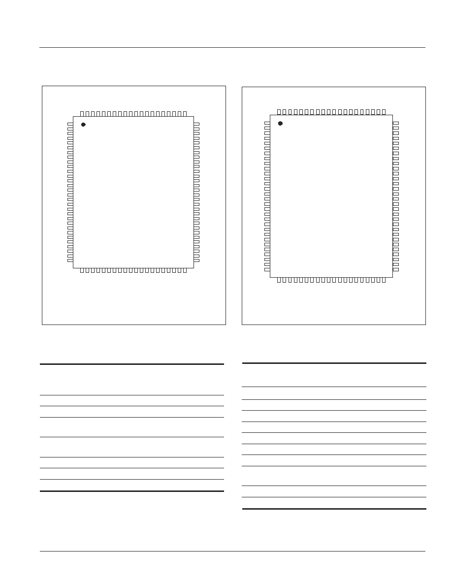
PIN CONFIGURATION
100-pin TQFP (T Version)
DQPb
DQb
DQb
V
DDQ
GND
DQb
DQb
DQb
DQb
GND
V
DDQ
DQb
DQb
GND
NC
V
DD
ZZ
DQa
DQa
V
DDQ
GND
DQa
DQa
DQa
DQa
GND
V
DDQ
DQa
DQa
DQPa
DQPc
DQc
DQc
V
DDQ
GND
DQc
DQc
DQc
DQc
GND
V
DDQ
DQc
DQc
NC
V
DD
NC
GND
DQd
DQd
V
DDQ
GND
DQd
DQd
DQd
DQd
GND
V
DDQ
DQd
DQd
DQPd
1
2
3
4
5
6
7
8
9
10
11
12
13
14
15
16
17
18
19
20
21
22
23
24
25
26
27
28
29
30
80
79
78
77
76
75
74
73
72
71
70
69
68
67
66
65
64
63
62
61
60
59
58
57
56
55
54
53
52
51
100 99 98 97 96 95 94 93 92 91 90 89 88 87 86 85 84 83 82 81
31 32 33 34 35 36 37 38 39 40 41 42 43 44 45
MODE
A
A
A
A
A1
A0
NC
NC
GND
V
DD
NC
A
A
A
A
A
A
A
A
46 47 48 49 50
A
A
CE
CE2
BWd
BWc
BWb
BWa
CE2
V
DD
GND
CLK
GW
BWE
OE
ADS
C
ADSP
ADV
A
A
6
Integrated Silicon Solution, Inc. -- www.issi.com --
1-800-379-4774
Rev. A
10/06/02
IS61LF25632T/D/J
IS61LF25636T/D/J
IS61LF51218T/D/J
ISSI
Æ
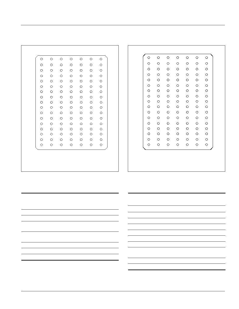
PIN CONFIGURATION
119-pin PBGA (Top View) (D Version)
256K x 36
PIN CONFIGURATION
119-pin PBGA (Top View) (J Version)
A
B
C
D
E
F
G
H
J
K
L
M
N
P
R
T
U
V
DDQ
NC
NC
DQc
DQc
V
DDQ
DQc
DQc
V
DDQ
DQd
DQd
V
DDQ
DQd
DQd
NC
NC
V
DDQ
A
CE2
A
DQPc
DQc
DQc
DQc
DQc
V
DD
DQd
DQd
DQd
DQd
DQPd
A
NC
NC
A
A
A
GND
GND
GND
BWc
GND
NC
GND
BWd
GND
GND
GND
MODE
A
NC
ADSP
ADSC
V
DD
NC
CE
OE
ADV
GW
V
DD
CLK
NC
BWE
A1
A0
V
DD
A
NC
A
A
A
GND
GND
GND
BWb
GND
NC
GND
BWa
GND
GND
GND
GND
A
NC
A
A
A
DQPb
DQb
DQb
DQb
DQb
V
DD
DQa
DQa
DQa
DQa
DQPa
A
NC
NC
V
DDQ
NC
NC
DQb
DQb
V
DDQ
DQb
DQb
V
DDQ
DQa
DQa
V
DDQ
DQa
DQa
NC
ZZ
V
DDQ
1
2
3
4
5
6
7
PIN DESCRIPTIONS
A0, A1
Synchronous Address Inputs. These
pins must tied to the two LSBs of the
address bus.
A
Synchronous Address Inputs
CLK
Synchronous Clock
ADSP
Synchronous Processor Address
Status
ADSC
Synchronous Controller Address
Status
ADV
Synchronous Burst Address Advance
BWa
-
BWd
Individual Byte Write Enable
BWE
Synchronous Byte Write Enable
TMS, TDI
JTAG Boundry Scan Pins
TCK, TDO
GW
Synchronous Global Write Enable
CE
, CE2
Synchronous Chip Enable
OE
Output Enable
DQa-DQd
Synchronous Data Input/Output
MODE
Burst Sequence Mode Selection
V
DD
+3.3V Power Supply
GND
Ground
V
DDQ
Isolated Output Buffer Supply:
+3.3V or 2.5V
ZZ
Snooze Enable
DQPa-DQPd
Parity Data I/O
A
B
C
D
E
F
G
H
J
K
L
M
N
P
R
T
U
V
DDQ
NC
NC
DQc
DQc
V
DDQ
DQc
DQc
V
DDQ
DQd
DQd
V
DDQ
DQd
DQd
NC
NC
V
DDQ
A
CE2
A
DQPc
DQc
DQc
DQc
DQc
V
DD
DQd
DQd
DQd
DQd
DQPd
A
NC
TMS
A
A
A
GND
GND
GND
BWc
GND
NC
GND
BWd
GND
GND
GND
MODE
A
TDI
ADSP
ADSC
V
DD
NC
CE
OE
ADV
GW
V
DD
CLK
NC
BWE
A1
A0
V
DD
A
TCK
A
A
A
GND
GND
GND
BWb
GND
NC
GND
BWa
GND
GND
GND
GND
A
TDO
A
A
A
DQPb
DQb
DQb
DQb
DQb
V
DD
DQa
DQa
DQa
DQa
DQPa
A
NC
NC
V
DDQ
NC
NC
DQb
DQb
V
DDQ
DQb
DQb
V
DDQ
DQa
DQa
V
DDQ
DQa
DQa
NC
ZZ
V
DDQ
1
2
3
4
5
6
7
256K x 36
Integrated Silicon Solution, Inc. -- www.issi.com --
1-800-379-4774
7
Rev.A
10/06/02
IS61LF25632T/D/J
IS61LF25636T/D/J
IS61LF51218T/D/J
ISSI
Æ
119-pin PBGA (Top View) (J Version)
A
B
C
D
E
F
G
H
J
K
L
M
N
P
R
T
U
V
DDQ
NC
NC
DQb
NC
V
DDQ
NC
DQb
V
DDQ
NC
DQb
V
DDQ
DQb
NC
NC
NC
V
DDQ
A
CE2
A
NC
DQb
NC
DQb
NC
V
DD
DQb
NC
DQb
NC
DQPb
A
A
TMS
A
A
A
GND
GND
GND
BWb
GND
NC
GND
GND
GND
GND
GND
MODE
A
TDI
ADSP
ADSC
V
DD
NC
CE
OE
ADV
GW
V
DD
CLK
NC
BWE
A1
A0
V
DD
NC
TCK
A
A
A
GND
GND
GND
GND
GND
NC
GND
BWa
GND
GND
GND
GND
A
TDO
A
A
A
DQPa
NC
DQa
NC
DQa
V
DD
NC
DQa
NC
DQa
NC
A
A
NC
V
DDQ
NC
NC
NC
DQa
V
DDQ
DQa
NC
V
DDQ
DQa
NC
V
DDQ
NC
DQa
NC
ZZ
V
DDQ
1 2 3 4 5 6 7
PIN CONFIGURATION
119-pin PBGA (Top View) (D Version)
512K x 18
PIN DESCRIPTIONS
A0, A1
Synchronous Address Inputs. These
pins must tied to the two LSBs of the
address bus.
A
Synchronous Address Inputs
CLK
Synchronous Clock
ADSP
Synchronous Processor Address
Status
ADSC
Synchronous Controller Address
Status
ADV
Synchronous Burst Address Advance
BWa
-
BWd
Individual Byte Write Enable
BWE
Synchronous Byte Write Enable
TMS, TDI
JTAG Boundry Scan Pins
TCK, TDO
GW
Synchronous Global Write Enable
CE
, CE2
Synchronous Chip Enable
OE
Output Enable
DQa-DQd
Synchronous Data Input/Output
MODE
Burst Sequence Mode Selection
V
DD
+3.3V Power Supply
GND
Ground
V
DDQ
Isolated Output Buffer Supply:
+3.3V or 2.5V
ZZ
Snooze Enable
DQPa-DQPd
Parity Data I/O
512K x 18
A
B
C
D
E
F
G
H
J
K
L
M
N
P
R
T
U
V
DDQ
NC
NC
DQb
NC
V
DDQ
NC
DQb
V
DDQ
NC
DQb
V
DDQ
DQb
NC
NC
NC
V
DDQ
A
CE2
A
NC
DQb
NC
DQb
NC
V
DD
DQb
NC
DQb
NC
DQPb
A
A
NC
A
A
A
GND
GND
GND
BWb
GND
NC
GND
GND
GND
GND
GND
MODE
A
NC
ADSP
ADSC
V
DD
NC
CE
OE
ADV
GW
V
DD
CLK
NC
BWE
A1
A0
V
DD
NC
NC
A
A
A
GND
GND
GND
GND
GND
NC
GND
BWa
GND
GND
GND
GND
A
NC
A
A
A
DQPa
NC
DQa
NC
DQa
V
DD
NC
DQa
NC
DQa
NC
A
A
NC
V
DDQ
NC
NC
NC
DQa
V
DDQ
DQa
NC
V
DDQ
DQa
NC
V
DDQ
NC
DQa
NC
ZZ
V
DDQ
1
2
3
4
5
6
7
8
Integrated Silicon Solution, Inc. -- www.issi.com --
1-800-379-4774
Rev. A
10/06/02
IS61LF25632T/D/J
IS61LF25636T/D/J
IS61LF51218T/D/J
ISSI
Æ
512K x 18
PIN DESCRIPTIONS
A0, A1
Synchronous Address Inputs. These
pins must tied to the two LSBs of the
address bus.
A
Synchronous Address Inputs
CLK
Synchronous Clock
ADSP
Synchronous Processor Address
Status
ADSC
Synchronous Controller Address
Status
ADV
Synchronous Burst Address Advance
BWa
-
BWd
Individual Byte Write Enable
BWE
Synchronous Byte Write Enable
TMS, TDI
JTAG Boundry Scan Pins
TCK, TDO
GW
Synchronous Global Write Enable
CE
, CE2,
CE2
Synchronous Chip Enable
OE
Output Enable
DQa-DQd
Synchronous Data Input/Output
MODE
Burst Sequence Mode Selection
V
DD
+3.3V Power Supply
GND
Ground
V
DDQ
Isolated Output Buffer Supply:
+3.3V or 2.5V
ZZ
Snooze Enable
DQPa-DQPd
Parity Data I/O
A
NC
NC
V
DDQ
GND
NC
DQPa
DQa
DQa
GND
V
DDQ
DQa
DQa
GND
NC
V
DD
ZZ
DQa
DQa
V
DDQ
GND
DQa
DQa
NC
NC
GND
V
DDQ
NC
NC
NC
A
A
CE
CE2
NC
NC
BWb
BWa
CE2
V
DD
GND
CLK
GW
BWE
OE
ADSC
ADSP
ADV
A
A
NC
NC
NC
V
DDQ
GND
NC
NC
DQb
DQb
GND
V
DDQ
DQb
DQb
GND
V
DD
NC
GND
DQb
DQb
V
DDQ
GND
DQb
DQb
DQPb
NC
GND
V
DDQ
NC
NC
NC
1
2
3
4
5
6
7
8
9
10
11
12
13
14
15
16
17
18
19
20
21
22
23
24
25
26
27
28
29
30
80
79
78
77
76
75
74
73
72
71
70
69
68
67
66
65
64
63
62
61
60
59
58
57
56
55
54
53
52
51
100 99 98 97 96 95 94 93 92 91 90 89 88 87 86 85 84 83 82 81
31 32 33 34 35 36 37 38 39 40 41 42 43 44 45
MODE
A
A
A
A
A1
A0
NC
NC
GND
V
DD
NC
A
A
A
A
A
A
A
A
46 47 48 49 50
100-Pin TQFP (T Version)
A
NC
NC
V
DDQ
GND
NC
DQPa
DQa
DQa
GND
V
DDQ
DQa
DQa
GND
NC
V
DD
ZZ
DQa
DQa
V
DDQ
GND
DQa
DQa
NC
NC
GND
V
DDQ
NC
NC
NC
A
A
CE
CE2
NC
NC
BWb
BWa
A
V
DD
GND
CLK
GW
BWE
OE
ADSC
ADSP
ADV
A
A
NC
NC
NC
V
DDQ
GND
NC
NC
DQb
DQb
GND
V
DDQ
DQb
DQb
GND
V
DD
NC
GND
DQb
DQb
V
DDQ
GND
DQb
DQb
DQPb
NC
GND
V
DDQ
NC
NC
NC
1
2
3
4
5
6
7
8
9
10
11
12
13
14
15
16
17
18
19
20
21
22
23
24
25
26
27
28
29
30
80
79
78
77
76
75
74
73
72
71
70
69
68
67
66
65
64
63
62
61
60
59
58
57
56
55
54
53
52
51
100 99 98 97 96 95 94 93 92 91 90 89 88 87 86 85 84 83 82 81
31 32 33 34 35 36 37 38 39 40 41 42 43 44 45
MODE
A
A
A
A
A1
A0
NC
NC
GND
V
DD
NC
NC
A
A
A
A
A
A
A
46 47 48 49 50
PIN CONFIGURATION
100-Pin TQFP (D Version)
512K x 18

Integrated Silicon Solution, Inc. -- www.issi.com --
1-800-379-4774
9
Rev.A
10/06/02
IS61LF25632T/D/J
IS61LF25636T/D/J
IS61LF51218T/D/J
ISSI
Æ
PARTIAL TRUTH TABLE
Function
GW
GW
GW
GW
GW
BWE
BWE
BWE
BWE
BWE
BWa
BWa
BWa
BWa
BWa
BWb
BWb
BWb
BWb
BWb
BWc
BWc
BWc
BWc
BWc
BWd
BWd
BWd
BWd
BWd
Read
H
H
X
X
X
X
Read
H
L
H
H
H
H
Write Byte 1
H
L
L
H
H
H
Write All Bytes
H
L
L
L
L
L
Write All Bytes
L
X
X
X
X
X
TRUTH TABLE
Address
Operation
Used
CE
CE
CE
CE
CE
CE2
CE2
CE2
CE2
CE2
CE2
ADSP
ADSP
ADSP
ADSP
ADSP ADSC
ADSC
ADSC
ADSC
ADSC
ADV
ADV
ADV
ADV
ADV
WRITE
WRITE
WRITE
WRITE
WRITE
OE
OE
OE
OE
OE
DQ
Deselected, Power-down
None
H
X
X
X
L
X
X
X
High-Z
Deselected, Power-down
None
L
X
H
L
X
X
X
X
High-Z
Deselected, Power-down
None
L
L
X
L
X
X
X
X
High-Z
Deselected, Power-down
None
L
X
H
H
L
X
X
X
High-Z
Deselected, Power-down
None
L
L
X
H
L
X
X
X
High-Z
Read Cycle, Begin Burst
External
L
H
L
L
X
X
X
X
Q
Read Cycle, Begin Burst
External
L
H
L
H
L
X
Read
X
Q
Write Cycle, Begin Burst
External
L
H
L
H
L
X
Write
X
D
Read Cycle, Continue Burst
Next
X
X
X
H
H
L
Read
L
Q
Read Cycle, Continue Burst
Next
X
X
X
H
H
L
Read
H
High-Z
Read Cycle, Continue Burst
Next
H
X
X
X
H
L
Read
L
Q
Read Cycle, Continue Burst
Next
H
X
X
X
H
L
Read
H
High-Z
Write Cycle, Continue Burst
Next
X
X
X
H
H
L
Write
X
D
Write Cycle, Continue Burst
Next
H
X
X
X
H
L
Write
X
D
Read Cycle, Suspend Burst
Current
X
X
X
H
H
H
Read
L
Q
Read Cycle, Suspend Burst
Current
X
X
X
H
H
H
Read
H
High-Z
Read Cycle, Suspend Burst
Current
H
X
X
X
H
H
Read
L
Q
Read Cycle, Suspend Burst
Current
H
X
X
X
H
H
Read
H
High-Z
Write Cycle, Suspend Burst
Current
X
X
X
H
H
H
Write
X
D
Write Cycle, Suspend Burst
Current
H
X
X
X
H
H
Write
X
D
10
Integrated Silicon Solution, Inc. -- www.issi.com --
1-800-379-4774
Rev. A
10/06/02
IS61LF25632T/D/J
IS61LF25636T/D/J
IS61LF51218T/D/J
ISSI
Æ
INTERLEAVED BURST ADDRESS TABLE (MODE = V
DDQ
or No Connect)
External Address
1st Burst Address
2nd Burst Address
3rd Burst Address
A1 A0
A1 A0
A1 A0
A1 A0
00
01
10
11
01
00
11
10
10
11
00
01
11
10
01
00
LINEAR BURST ADDRESS TABLE (MODE = GND
Q
)
ABSOLUTE MAXIMUM RATINGS
(1)
Symbol
Parameter
Value
Unit
T
STG
Storage Temperature
≠55 to +150
∞C
P
D
Power Dissipation
1.6
W
I
OUT
Output Current (per I/O)
100
mA
V
IN
, V
OUT
Voltage Relative to GND for I/O Pins
≠0.5 to V
DDQ
+ 0.3
V
V
IN
Voltage Relative to GND for
≠0.5 to V
DD
+ 0.5
V
for Address and Control Inputs
V
DD
Voltage on Vdd Supply Relatiive to GND
≠0.5 to 4.6
V
Notes:
1. Stress greater than those listed under ABSOLUTE MAXIMUM RATINGS may cause permanent damage to the device. This is a
stress rating only and functional operation of the device at these or any other conditions above those indicated in the operational
sections of this specification is not implied. Exposure to absolute maximum rating conditions for extended periods may affect
reliability.
2. This device contains circuity to protect the inputs against damage due to high static voltages or electric fields; however, precautions
may be taken to avoid application of any voltage higher than maximum rated voltages to this high-impedance circuit.
3. This device contains circuitry that will ensure the output devices are in High-Z at power up.
0,0
1,0
0,1
A1', A0' = 1,1

Integrated Silicon Solution, Inc. -- www.issi.com --
1-800-379-4774
11
Rev.A
10/06/02
IS61LF25632T/D/J
IS61LF25636T/D/J
IS61LF51218T/D/J
ISSI
Æ
OPERATING RANGE
Range
Ambient Temperature
V
DD
V
DDQ
Commercial
0∞C to +70∞C
3.3V,
+10%, ≠5%
2.375
≠
3.6V
Industrial
≠40∞C to +85∞C
3.3V,
+10%, ≠5%
2.375
≠
3.6V
DC ELECTRICAL CHARACTERISTICS
(1)
(Over Operating Range)
Symbol Parameter
Test Conditions
Min.
Max.
Unit
V
OH
Output HIGH Voltage
I
OH
= ≠1.0 mA, V
DDQ
= 2.5V
2.0
--
V
I
OH
= ≠4.0 mA, V
DDQ
= 3.3V
2.4
--
V
V
OL
Output LOW Voltage
I
OL
= 1.0 mA, V
DDQ
= 2.5V
--
0.4
V
I
OL
= 8.0 mA, V
DDQ
= 3.3V
--
0.4
V
V
IH
Input HIGH Voltage
V
DDQ
= 2.5V
1.7
V
DD
+ 0.3
V
V
DDQ
= 3.3V
2.0
V
DD
+ 0.3
V
V
IL
Input LOW Voltage
V
DDQ
= 2.5V
≠0.3
0.7
V
V
DDQ
= 3.3V
≠0.3
0.8
V
I
LI
Input Leakage Current
GND
V
IN
V
DDQ
(2)
Com.
≠5
5
µA
Ind.
≠5
5
I
LO
Output Leakage Current
GND
V
OUT
V
DDQ
,
OE
= V
IH
Com.
≠5
5
µA
Ind.
≠5
5
POWER SUPPLY CHARACTERISTICS
(Over Operating Range)
6.5
7.5
Symbol Parameter
Test Conditions
Max.
Max.
Unit
I
CC
AC Operating
Device Selected,
Com.
110
100
mA
Supply Current
All Inputs < V
IL
or > V
IH
Ind.
120
110
mA
OE
= V
IH
, ZZ < V
IL
Cycle Time
t
KC
min.
I
SB
Standby Current
Device Deselected,
Com.
55
55
mA
V
DD
= Max.,
Ind.
60
60
mA
All Inputs < V
IL
or > V
IH
ZZ < V
IL
, f = fmax
I
SBI
Standby Current
Device Deselected,
Com.
30
30
mA
CMOS Input
V
DD
= Max.,
Ind.
40
40
mA
V
IN
GND + 0.2V or
V
DD
-0.2V
f = 0
Notes:
1. The MODE pin should be tied to V
DD
or GND. It exhibits ±30 µA maximum leakage current when tied to< GND + 0.2V
or
V
DD
≠ 0.2V.
12
Integrated Silicon Solution, Inc. -- www.issi.com --
1-800-379-4774
Rev. A
10/06/02
IS61LF25632T/D/J
IS61LF25636T/D/J
IS61LF51218T/D/J
ISSI
Æ
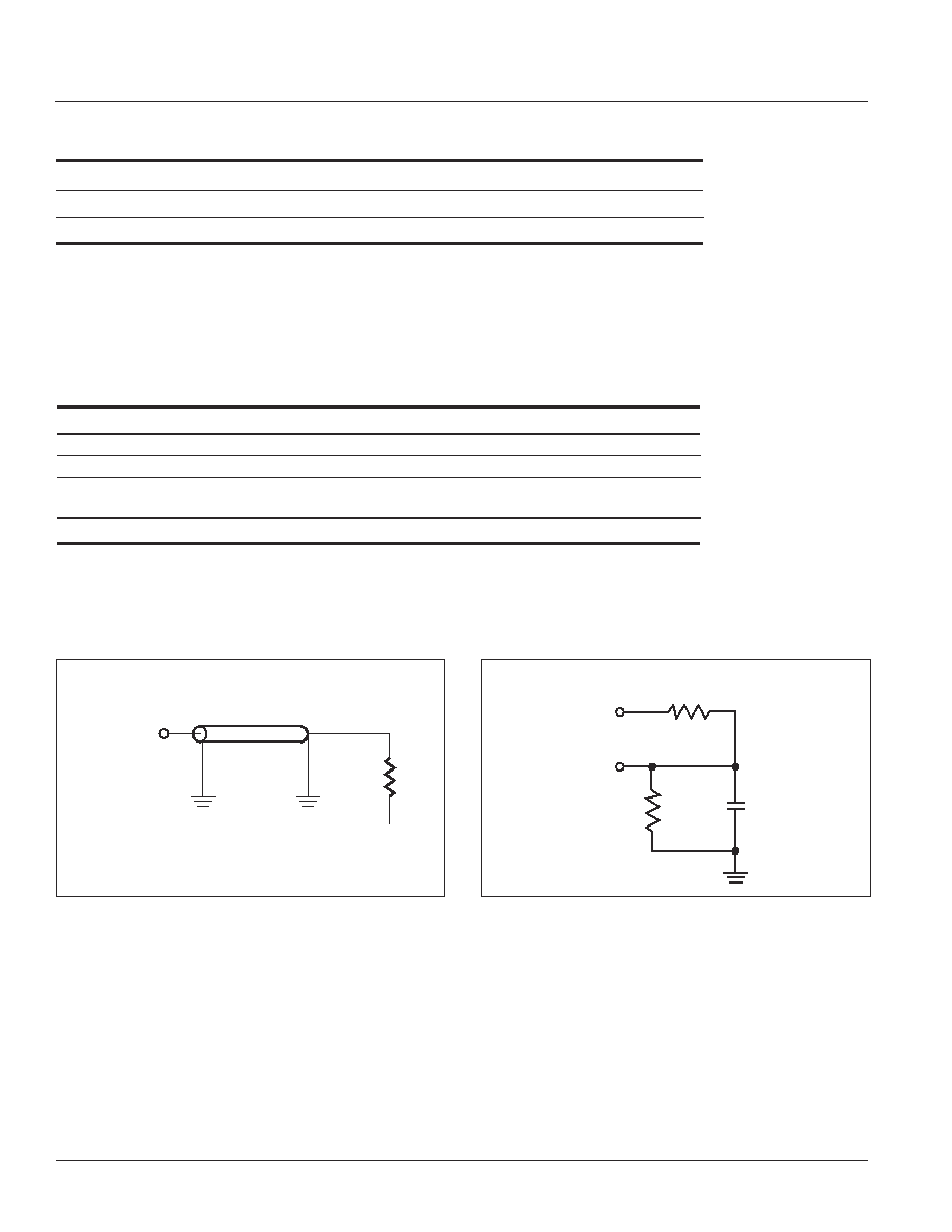
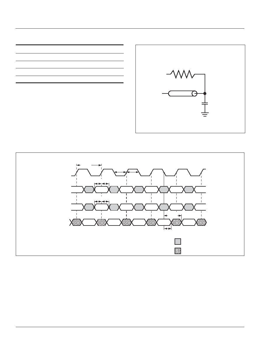
3.3V I/O AC TEST CONDITIONS
Parameter
Unit
Input Pulse Level
0V to 3.0V
Input Rise and Fall Times
1ns
Input and Output Timing
1.5V
and Reference Level
Output Load
See Figures 1 and 2
Figure 1
Figure 2
CAPACITANCE
(1,2)
Symbol
Parameter
Conditions
Max.
Unit
C
IN
Input Capacitance
V
IN
= 0V
6
pF
C
OUT
Input/Output Capacitance
V
OUT
= 0V
8
pF
Notes:
1. Tested initially and after any design or process changes that may affect these parameters.
2. Test conditions: T
A
= 25∞C, f = 1 MHz, Vdd = 3.3V.
3.3V I/O OUTPUT LOAD EQUIVALENT
Z
O
= 50
1.5V
50
OUTPUT
317
5 pF
Including
jig and
scope
351
OUTPUT
+3.3V
Integrated Silicon Solution, Inc. -- www.issi.com --
1-800-379-4774
13
Rev.A
10/06/02
IS61LF25632T/D/J
IS61LF25636T/D/J
IS61LF51218T/D/J
ISSI
Æ
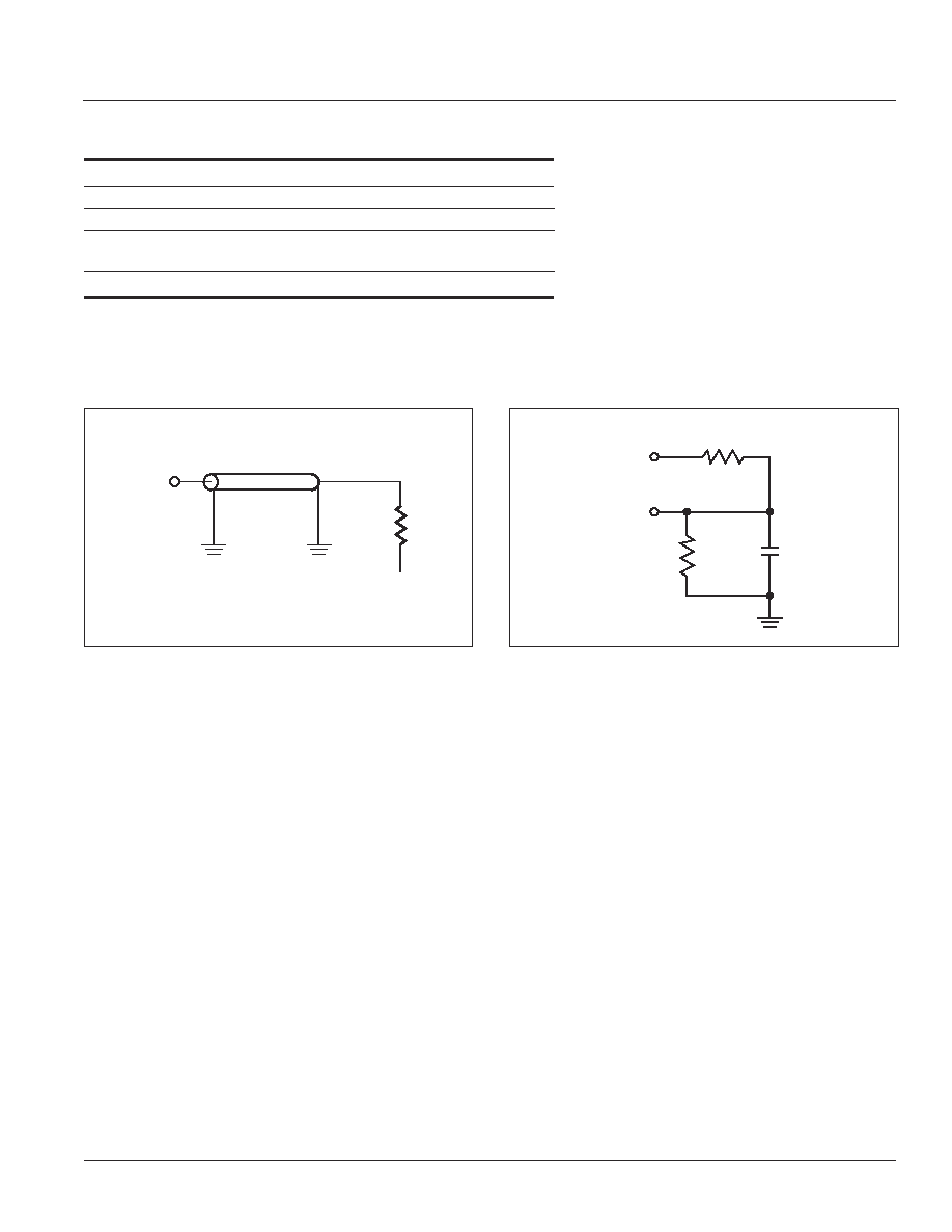
2.5V I/O AC TEST CONDITIONS
Parameter
Unit
Input Pulse Level
0V to 2.5V
Input Rise and Fall Times
1 ns
Input and Output Timing
1.25V
and Reference Level
Output Load
See Figures 3 and 4
Figure 3
Figure 4
2.5V I/O OUTPUT LOAD EQUIVALENT
Z
O
= 50
1.25V
50
OUTPUT
1,667
5 pF
Including
jig and
scope
1,538
OUTPUT
+2.5V

14
Integrated Silicon Solution, Inc. -- www.issi.com --
1-800-379-4774
Rev. A
10/06/02
IS61LF25632T/D/J
IS61LF25636T/D/J
IS61LF51218T/D/J
ISSI
Æ
READ/WRITE CYCLE SWITCHING CHARACTERISTICS
(Over Operating Range)
6.5
7.5
Symbol
Parameter
Min. Max.
Min. Max.
Unit
f
MAX
Clock Frequency
--
133
--
117
MHz
t
KC
Cycle Time
7.5
--
8.5
--
ns
t
KH
Clock High Pulse Width
2.2
--
2.5
--
ns
t
KL
Clock Low Pulse Width
2.2
--
2.5
--
ns
t
KQ
Clock Access Time
--
6.5
--
7.5
ns
t
KQX
(1)
Clock High to Output Invalid
2
--
2
--
ns
t
KQLZ
(1,2)
Clock High to Output Low-Z
0
--
0
--
ns
t
KQHZ
(1,2)
Clock High to Output High-Z
--
3.5
--
3.5
ns
t
OEQ
Output Enable to Output Valid
--
3.5
--
3.5
ns
t
OELZ
(1,2)
Output Enable to Output Low-Z
0
--
0
--
ns
t
OEHZ
(1,2)
Output Enable to Output High-Z
--
3.5
--
3.5
ns
t
AS
Address Setup Time
1.5
--
1.8
--
ns
t
SS
Address Status Setup Time
1.5
--
1.8
--
ns
t
WS
Write Setup Time
1.5
--
1.8
--
ns
t
CES
Chip Enable Setup Time
1.5
--
1.8
--
ns
t
AVS
Address Advance Setup Time
1.5
--
1.8
--
ns
t
AH
Address Hold Time
0.5
--
0.5
--
ns
t
SH
Address Status Hold Time
0.5
--
0.5
--
ns
t
WH
Write Hold Time
0.5
--
0.5
--
ns
t
CEH
Chip Enable Hold Time
0.5
--
0.5
--
ns
t
AVH
Address Advance Hold Time
0.5
--
0.5
--
ns
Note:
1. Guaranteed but not 100% tested. This parameter is periodically sampled.
2. Tested with load in Figure 2.
Integrated Silicon Solution, Inc. -- www.issi.com --
1-800-379-4774
15
Rev.A
10/06/02
IS61LF25632T/D/J
IS61LF25636T/D/J
IS61LF51218T/D/J
ISSI
Æ
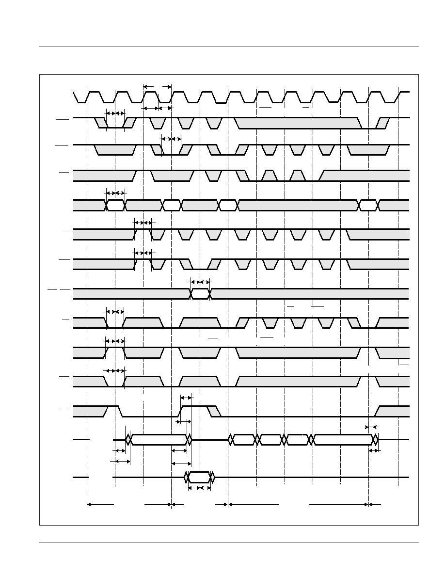
READ/WRITE CYCLE TIMING
Single Read
Flow-through
Single Write
High-Z
High-Z
DATA
OUT
DATA
IN
OE
CE2
CE2
CE
BWd-BWa
BWE
GW
A
ADV
ADSC
ADSP
CLK
RD1
WR1
WR1
1a
1a
2a
2b
2c
2d
Unselected
Burst Read
t
KQX
t
KC
t
KL
t
KH
t
SS
t
SH
ADSP is blocked by CE inactive
t
SS
t
SH
t
AS
t
AH
t
WS
t
WH
t
WS
t
WH
t
WS
t
WH
RD2
RD3
t
CES
t
CEH
t
CES
t
CEH
t
CES
t
CEH
CE2 and CE2 only sampled with ADSP or ADSC
CE Masks ADSP
Unselected with CE2
t
OEQX
t
KQ
t
OEHZ
t
KQX
t
KQHZ
t
DS
t
DH
t
KQHZ
t
KQLZ

16
Integrated Silicon Solution, Inc. -- www.issi.com --
1-800-379-4774
Rev. A
10/06/02
IS61LF25632T/D/J
IS61LF25636T/D/J
IS61LF51218T/D/J
ISSI
Æ
WRITE CYCLE SWITCHING CHARACTERISTICS
(Over Operating Range)
6.5
7.5
Symbol
Parameter
Min. Max.
Min. Max.
Unit
t
KC
Cycle Time
7.5
--
8.5
--
ns
t
KH
Clock High Pulse Width
2.0
--
2.5
--
ns
t
KL
Clock Low Pulse Width
2.2
--
2.5
--
ns
t
AS
Address Setup Time
1.5
--
1.8
--
ns
t
SS
Address Status Setup Time
1.5
--
1.8
--
ns
t
WS
Write Setup Time
1.5
--
1.8
--
ns
t
DS
Data In Setup Time
1.5
--
1.8
--
ns
t
CES
Chip Enable Setup Time
1.5
--
1.8
--
ns
t
AVS
Address Advance Setup Time
1.5
--
1.8
--
ns
t
AH
Address Hold Time
0.5
--
0.5
--
ns
t
SH
Address Status Hold Time
0.5
--
0.5
--
ns
t
DH
Data In Hold Time
0.5
--
0.5
--
ns
t
WH
Write Hold Time
0.5
--
0.5
--
ns
t
CEH
Chip Enable Hold Time
0.5
--
0.5
--
ns
t
AVH
Address Advance Hold Time
0.5
--
0.5
--
ns
Integrated Silicon Solution, Inc. -- www.issi.com --
1-800-379-4774
17
Rev.A
10/06/02
IS61LF25632T/D/J
IS61LF25636T/D/J
IS61LF51218T/D/J
ISSI
Æ
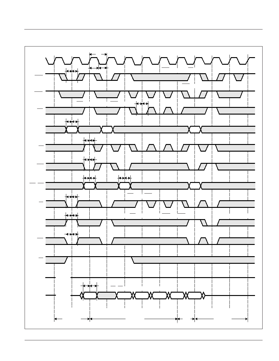
WRITE CYCLE TIMING
Single Write
DATA
OUT
DATA
IN
OE
CE2
CE2
CE
BWd-BWa
BWE
GW
A17-A0
ADV
ADSC
ADSP
CLK
WR1
WR2
Unselected
Burst Write
t
KC
t
KL
t
KH
t
SS
t
SH
t
AS
t
AH
t
WS
t
WH
t
WS
t
WH
WR3
t
CES
t
CEH
t
CES
t
CEH
t
CES
t
CEH
CE2 and CE3 only sampled with ADSP or ADSC
CE1 Masks ADSP
Unselected with CE2
ADSC initiate Write
ADSP is blocked by CE1 inactive
t
AVH
t
AVS
ADV must be inactive for ADSP Write
WR1
WR2
t
WS
t
WH
WR3
t
WS
t
WH
High-Z
High-Z
1a
3a
t
DS
t
DH
BW4-BW1 only are applied to first cycle of WR2
Write
2c
2d
2b
2a
18
Integrated Silicon Solution, Inc. -- www.issi.com --
1-800-379-4774
Rev. A
10/06/02
IS61LF25632T/D/J
IS61LF25636T/D/J
IS61LF51218T/D/J
ISSI
Æ
SLEEP MODE TIMING
Don't Care
Deselect or Read Only
Deselect or Read Only
t
RZZI
CLK
ZZ
Isupply
All Inputs
(except ZZ)
Outputs
(Q)
I
SB2
ZZ setup cycle
ZZ recovery cycle
Normal
operation
cycle
t
PDS
t
PUS
t
ZZI
High-Z
SLEEP MODE ELECTRICAL CHARACTERISTICS
Symbol
Parameter
Conditions
Min.
Max.
Unit
I
SB
2
Current during SLEEP MODE
ZZ
V
IH
Com.
--
30
mA
ZZ
V
IH
Ind.
--
40
t
PDS
ZZ active to input ignored
2
--
cycle
t
PUS
ZZ inactive to input sampled
2
--
cycle
t
ZZI
ZZ active to SLEEP current
2
--
cycle
t
RZZI
ZZ inactive to exit SLEEP current
0
--
ns
Integrated Silicon Solution, Inc. -- www.issi.com --
1-800-379-4774
19
Rev.A
10/06/02
IS61LF25632T/D/J
IS61LF25636T/D/J
IS61LF51218T/D/J
ISSI
Æ
31 30 29
. . .
2 1 0
2 1 0
0
x
. . . . .
2 1 0
Bypass Register
Instruction Register
Identification Register
Boundary Scan Register*
TAP CONTROLLER
Selection Circuitry
Selection Circuitry
TDO
TDI
TCK
TMS
IEEE 1149.1 Serial Boundary Scan (JTAG)
The IS61LF25636T/D/J and IS61LF51218T/D/JT/D/JT/D/
J have a serial boundary scan Test Access Port (TAP) in the
PBGA package only. (Not available in TQFP package or
with the IS61LPS25632T/D/J.) This port operates in accor-
dance with IEEE Standard 1149.1-1900, but does not
include all functions required for full 1149.1 compliance.
These functions from the IEEE specification are excluded
because they place added delay in the critical speed path
of the SRAM. The TAP controller operates in a manner that
does not conflict with the performance of other devices
using 1149.1 fully compliant TAPs. The TAP operates using
JEDEC standard 2.5V I/O logic levels.
Disabling the JTAG Feature
The SRAM can operate without using the JTAG feature. To
disable the TAP controller, TCK must be tied LOW (GND)
to prevent clocking of the device. TDI and TMS are
internally pulled up and may be disconnected. They may
alternately be connected to V
DD
through a pull-up resistor.
TDO should be left disconnected. On power-up, the device
will start in a reset state which will not interfere with the
device operation.
Test Access Port (TAP) - Test Clock
The test clock is only used with the TAP controller. All
inputs are captured on the rising edge of TCK and outputs
are driven from the falling edge of TCK.
Test Mode Select (TMS)
The TMS input is used to send commands to the TAP
controller and is sampled on the rising edge of TCK. This
pin may be left disconnected if the TAP is not used. The
pin is internally pulled up, resulting in a logic HIGH level.
Test Data-In (TDI)
The TDI pin is used to serially input information to the
registers and can be connected to the input of any register.
The register between TDI and TDO is chosen by the
instruction loaded into the TAP instruction register. For
information on instruction register loading, see the TAP
Controller State Diagram. TDI is internally pulled up and
can be disconnected if the TAP is unused in an application.
TDI is connected to the Most Significant Bit (MSB) on any
register.
TAP CONTROLLER BLOCK DIAGRAM

20
Integrated Silicon Solution, Inc. -- www.issi.com --
1-800-379-4774
Rev. A
10/06/02
IS61LF25632T/D/J
IS61LF25636T/D/J
IS61LF51218T/D/J
ISSI
Æ
Test Data Out (TDO)
The TDO output pin is used to serially clock data-out from
the registers. The output is active depending on the current
state of the TAP state machine (see TAP Controller State
Diagram). The output changes on the falling edge of TCK
and TDO is connected to the Least Significant Bit (LSB) of
any register.
Performing a TAP Reset
A Reset is performed by forcing TMS HIGH (V
DD
) for five
rising edges of TCK. RESET may be performed while the
SRAM is operating and does not affect its operation. At
power-up, the TAP is internally reset to ensure that TDO
comes up in a high-Z state.
TAP Registers
Registers are connected between the TDI and TDO pins
and allow data to be scanned into and out of the SRAM test
circuitry. Only one register can be selected at a time
through the instruction registers. Data is serially loaded into
the TDI pin on the rising edge of TCK and output on the TDO
pin on the falling edge of TCK.
Instruction Register
Three-bit instructions can be serially loaded into the in-
struction register. This register is loaded when it is placed
between the TDI and TDO pins. (See TAP Controller Block
Diagram) At power-up, the instruction register is loaded
with the IDCODE instruction. It is also loaded with the
IDCODE instruction if the controller is placed in a reset
state as previously described.
When the TAP controller is in the CaptureIR state, the two
least significant bits are loaded with a binary "01" pattern to
allow for fault isolation of the board level serial test path.
Bypass Register
To save time when serially shifting data through registers,
it is sometimes advantageous to skip certain states. The
bypass register is a single-bit register that can be placed
between TDI and TDO pins. This allows data to be shifted
through the SRAM with minimal delay. The bypass register
is set LOW (GND) when the BYPASS instruction is ex-
ecuted.
Boundary Scan Register
The boundary scan register is connected to all input and
output pins on the SRAM. Several no connect (NC) pins are
also included in the scan register to reserve pins for higher
density devices. The x36 configuration has a 70-bit-long
register and the x18 configuration has a 51-bit-long regis-
ter. The boundary scan register is loaded with the contents
of the RAM Input and Output ring when the TAP controller
is in the Capture-DR state and then placed between the TDI
and TDO pins when the controller is moved to the Shift-DR
state. The EXTEST, SAMPLE/PRELOAD and SAMPLE Z
instructions can be used to capture the contents of the
Input and Output ring.
The Boundary Scan Order tables show the order in which
the bits are connected. Each bit corresponds to one of the
bumps on the SRAM package. The MSB of the register is
connected to TDI, and the LSB is connected to TDO.
Scan Register Sizes
Register Name
Bit Size (x18)
Bit Size (x36)
Instruction
3
3
Bypass
1
1
ID
32
32
Boundary Scan
51
70
Integrated Silicon Solution, Inc. -- www.issi.com --
1-800-379-4774
21
Rev.A
10/06/02
IS61LF25632T/D/J
IS61LF25636T/D/J
IS61LF51218T/D/J
ISSI
Æ
IDENTIFICATION (ID) REGISTER
The ID Register is a 32-bit register that is loaded with a
device and vendor specific 32-bit code when the controller
is put in Capture-DR state with the IDCODE command
loaded in the Instruction Register. The code is loaded from
a 32-bit on-chip ROM. It describes various attributes of the
RAM as indicated below. The register is then placed
between the TDI and TDO pins when the controller is moved
into Shift-DR state. Bit 0 in the register is the LSB and the
first to reach TDO when shifting begins.
ID REGISTER CONTENTS
Die
Vendor
ISSI Technology
Revision
Part Configuration
Defomotopm
JEDEC Vendor
Code
ID Code
Presence Register
Part # 31 30 29 28 27 26 25 24 23 22 21 20 19 18 17 16 15 14 13 12 11 10 9
8
7
6
5
4
3
2
1
0
256K
X X X X
0
0
1
1
0
0
0
1 0
0 X
X X X
X X
0
0
0
1
1
0
1
0
1
0
1
1
512K
X X X X
0
0
1
1
1
0
0
0 1
1 X
X X X
X X
0
0
0
1
1
0
1
0
1
0
1
1
SAMPLE Z
The SAMPLE Z instruction causes the boundary scan
register to be connected between the TDI and TDO pins
when the TAP controller is in a Shift-DR state. It also places
all SRAM outputs into a High-Z state.
SAMPLE/PRELOAD
SAMPLE/PRELOAD is a 1149.1 mandatory instruction.
The PRELOAD portion of this instruction is not imple-
mented, so the TAP controller is not fully 1149.1 compliant.
When the SAMPLE/PRELOAD instruction is loaded to the
instruction register and the TAP controller is in the Capture-
DR state, a snapshot of data on the inputs and output pins
is captured in the boundary scan register.
It is important to realize that the TAP controller clock
operates at a frequency up to 10 MHz, while the SRAM
clock runs more than an order of magnitude faster. Because
of the clock frequency differences, it is possible that during
the Capture-DR state, an input or output will under-go a
transition. The TAP may attempt a signal capture while in
transition (metastable state). The device will not be harmed,
but there is no guarantee of the value that will be captured
or repeatable results.
To guarantee that the boundary scan register will capture
the correct signal value, the SRAM signal must be stabi-
lized long enough to meet the TAP controller's capture set-
up plus hold times (t
CS
and t
CH
). To insure that the SRAM
clock input is captured correctly, designs need a way to stop
(or slow) the clock during a SAMPLE/PRELOAD instruc-
tion. If this is not an issue, it is possible to capture all other
signals and simply ignore the value of the CLK and
CLK
captured in the boundary scan register.
Once the data is captured, it is possible to shift out the data
by putting the TAP into the Shift-DR state. This places the
boundary scan register between the TDI and TDO pins.
Note that since the PRELOAD part of the command is not
implemented, putting the TAP into the Update to the Update-DR
state while performing a SAMPLE/PRELOAD instruction will
have the same effect as the Pause-DR command.
Bypass
When the BYPASS instruction is loaded in the instruction
register and the TAP is placed in a Shift-DR state, the
bypass register is placed between the TDI and TDO pins.
The advantage of the BYPASS instruction is that it shortens
the boundary scan path when multiple devices are con-
nected together on a board.
Reserved
These instructions are not implemented but are reserved for
future use. Do not use these instructions.
22
Integrated Silicon Solution, Inc. -- www.issi.com --
1-800-379-4774
Rev. A
10/06/02
IS61LF25632T/D/J
IS61LF25636T/D/J
IS61LF51218T/D/J
ISSI
Æ
INSTRUCTION CODES
Code
Instruction
Description
001
IDCODE
Loads the ID register with the vendor ID code and places the register between TDI
and TDO. This operation does not affect SRAM operation.
010
SAMPLE Z
Captures the Input/Output contents. Places the boundary scan register between
TDI and TDO. Forces all SRAM output drivers to a High-Z state.
011
RESERVED
Do Not Use: This instruction is reserved for future use.
100
SAMPLE/PRELOAD
Captures the Input/Output ring contents. Places the boundary scan register be-
tween TDI and TDO. Does not affect the SRAM operation. This instruction does not
implement 1149.1 preload function and is therefore not 1149.1 compliant.
101
RESERVED
Do Not Use: This instruction is reserved for future use.
110
RESERVED
Do Not Use: This instruction is reserved for future use.
111
BYPASS
Places the bypass register between TDI and TDO. This operation does not
affect SRAM operation.
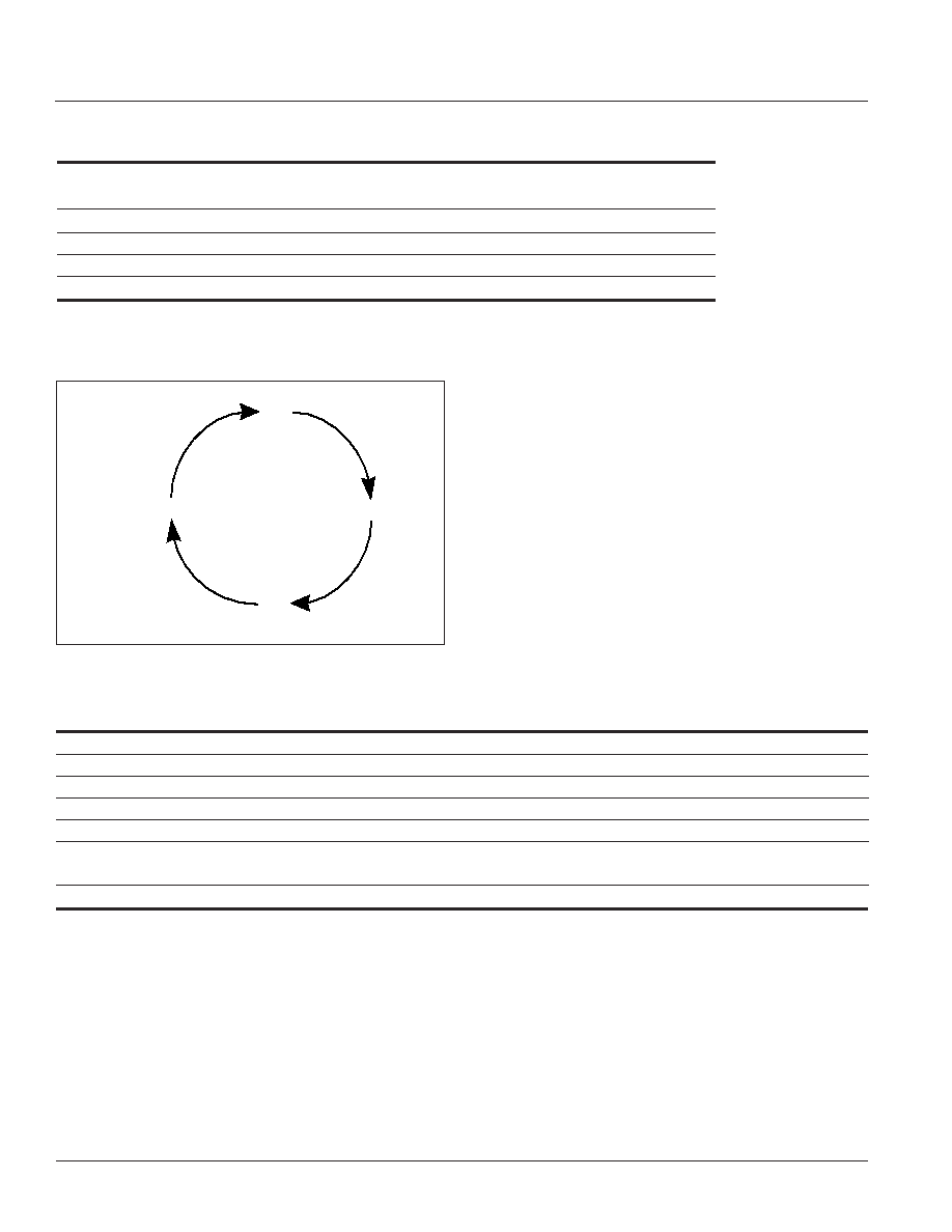
TAP CONTROLLER STATE DIAGRAM
Select DR
Capture DR
Shift DR
Exit1 DR
Pause DR
Exit2 DR
Update DR
Select IR
Capture IR
Shift IR
Exit1 IR
Pause IR
Exit2 IR
Update IR
Test Logic Reset
Run Test/Idle
1
1
1
1
1
1
1
1
1
1
1
1
1
1
0
0
0
0
1
0
0
0
0
0
0
0
0
0
0
0
1
0

Integrated Silicon Solution, Inc. -- www.issi.com --
1-800-379-4774
23
Rev.A
10/06/02
IS61LF25632T/D/J
IS61LF25636T/D/J
IS61LF51218T/D/J
ISSI
Æ
TAP ELECTRICAL CHARACTERISTICS Over the Operating Range
(1,2)
Symbol
Parameter
Test Conditions
Min.
Max.
Units
V
OH1
Output HIGH Voltage
I
OH
= ≠2.0 mA
1.7
--
V
V
OH2
Output HIGH Voltage
I
OH
= ≠100 mA
2.1
--
V
V
OL1
Output LOW Voltage
I
OL
= 2.0 mA
--
0.7
V
V
OL2
Output LOW Voltage
I
OL
= 100 mA
--
0.2
V
V
IH
Input HIGH Voltage
1.7
V
DD
+0.3
V
V
IL
Input LOW Voltage
I
OLT
= 2mA
≠0.3
0.7
V
I
X
Input Load Current
GND
V I
V
DDQ
≠5
5
mA
Notes:
1. All Voltage referenced to Ground.
2. Overshoot: V
IH
(AC)
V
DD
+1.5V for t
t
TCYC
/2,
Undershoot:V
IL
(AC)
0.5V for t
t
TCYC
/2,
Power-up: V
IH
< 2.6V and V
DD
< 2.4V and V
DDQ
< 1.4V for t < 200 ms.
TAP AC ELECTRICAL CHARACTERISTICS
(1)
(Over Operating Range)
Symbol
Parameter
Min.
Max.
Unit
t
TCYC
TCK Clock cycle time
100
--
ns
f
TF
TCK Clock frequency
--
10
MHz
t
TH
TCK Clock HIGH
40
--
ns
t
TL
TCK Clock LOW
40
--
ns
t
TMSS
TMS setup to TCK Clock Rise
10
--
ns
t
TDIS
TDI setup to TCK Clock Rise
10
--
ns
t
CS
Capture setup to TCK Rise
10
--
ns
t
TMSH
TMS hold after TCK Clock Rise
10
--
ns
t
TDIH
TDI Hold after Clock Rise
10
--
ns
t
CH
Capture hold after Clock Rise
10
--
ns
t
TDOV
TCK LOW to TDO valid
--
20
ns
t
TDOX
TCK LOW to TDO invalid
0
--
ns
Notes:
1. t
CS
and t
CH
refer to the set-up and hold time requirements of latching data from the boundary scan register.
2. Test conditions are specified using the load in TAP AC test conditions. t
R
/t
F
= 1 ns.
24
Integrated Silicon Solution, Inc. -- www.issi.com --
1-800-379-4774
Rev. A
10/06/02
IS61LF25632T/D/J
IS61LF25636T/D/J
IS61LF51218T/D/J
ISSI
Æ
TAP TIMING
TAP OUTPUT LOAD EQUIVALENT
TAP AC TEST CONDITIONS
Input pulse levels
0 to 2.5V
Input rise and fall times
1ns
Input timing reference levels
1.25V
Output reference levels
1.25V
Test load termination supply voltage
1.25V
20 pF
TDO
GND
50
1.25V
Z
0
= 50
DON'T CARE
UNDEFINED
TCK
TMS
TDI
TDO
t
THTL
t
TLTH
t
THTH
t
MVTH
t
THMX
t
DVTH
t
THDX
1 2 3 4 5 6
t
TLOX
t
TLOV

Integrated Silicon Solution, Inc. -- www.issi.com --
1-800-379-4774
25
Rev.A
10/06/02
IS61LF25632T/D/J
IS61LF25636T/D/J
IS61LF51218T/D/J
ISSI
Æ
BOUNDARY SCAN ORDER (256K X 36)
Signal Bump
Signal Bump
Signal Bump
Signal Bump
Bit #
Name
ID
Bit #
Name
ID
Bit #
Name
ID
Bit #
Name
ID
1
A
2R
19
DQb
7G
37
BWa
5L
55
DQd
2K
2
A
3T
20
DQb
6F
38
BWb
5G
56
DQd
1L
3
A
4T
21
DQb
7E
39
BWc
3G
57
DQd
2M
4
A
5T
22
DQb
7D
40
BWd
3L
58
DQd
1N
5
A
6R
23
DQb
7H
41
CE2
2B
59
DQd
1P
6
A
3B
24
DQb
6G
42
CE
4E
60
DQd
1K
7
A
5B
25
DQb
6E
43
A
3A
61
DQd
2L
8
DQa
6P
26
DQb
6D
44
A
2A
62
DQd
2N
9
DQa
7N
27
A
6A
45
DQc
2D
63
DQd
2P
10
DQa
6M
28
A
5A
46
DQc
1E
64
MODE
3R
11
DQa
7L
29
ADV
4G
47
DQc
2F
65
A
2C
12
DQa
6K
30
ADSP
4A
48
DQc
1G
66
A
3C
13
DQa
7P
31
ADSC
4B
49
DQc
2H
67
A
5C
14
DQa
6N
32
OE
4F
50
DQc
1D
68
A
6C
15
DQa
6L
33
BWE
4M
51
DQc
2E
69
A1
4N
16
DQa
7K
34
GW
4H
52
DQc
2G
70
A0
4P
17
ZZ
7T
35
CLK
4K
53
DQc
1H
18
DQb
6H
36
A
6B
54
NC
5R
BOUNDARY SCAN ORDER (512K X 18)
Signal Bump
Signal Bump
Signal Bump
Signal Bump
Bit #
Name
ID
Bit #
Name
ID
Bit #
Name
ID
Bit #
Name
ID
1
A
2R
14
DQa
7G
27
CLK
4K
40
DQb
2K
2
A
2T
15
DQa
6F
28
A
6B
41
DQb
1L
3
A
3T
16
DQa
7E
29
BWa
5L
42
DQb
2M
4
A
5T
17
DQa
6D
30
BWb
3G
43
DQb
1N
5
A
6R
18
A
6T
31
CE2
2B
44
DQb
2P
6
A
3B
19
A
6A
32
CE
4E
45
MODE
3R
7
A
5B
20
A
5A
33
A
3A
46
A
2C
8
DQa
7P
21
ADV
4G
34
A
2A
47
A
3C
9
DQa
6N
22
ADSP
4A
35
DQb
1D
48
A
5C
10
DQa
6L
23
ADSC
4B
36
DQb
2E
49
A
6C
11
DQa
7K
24
OE
4F
37
DQb
2G
50
A1
4N
12
ZZ
7T
25
BWE
4M
38
DQb
1H
51
A0
4P
13
DQa
6H
26
GW
4H
39
NC
5R

26
Integrated Silicon Solution, Inc. -- www.issi.com --
1-800-379-4774
Rev. A
10/06/02
IS61LF25632T/D/J
IS61LF25636T/D/J
IS61LF51218T/D/J
ISSI
Æ
ORDERING INFORMATION
Commercial Range: 0∞C to +70∞C
Speed
Order Part Number
Package
6.5 ns
IS61LF25632T-6.5TQ
TQFP
IS61LF25632D-6.5TQ
TQFP
7.5 ns
IS61LF25632T-7.5TQ
TQFP
IS61LF25632D-7.5TQ
TQFP
IS61LF25632D-7.5B
PBGA
Industrial Range: ≠40∞C to +85∞C
Speed
Order Part Number
Package
6.5 ns
IS61LF25632T-6.5TQI
TQFP
IS61LF25632D-6.5TQI
TQFP
7.5 ns
IS61LF25632T-7.5TQI
TQFP
IS61LF25632D-7.5TQI
TQFP
Industrial Range: ≠40∞C to +85∞C
Speed
Order Part Number
Package
6.5 ns
IS61LF25636T-6.5TQI
TQFP
IS61LF25636D-6.5TQI
TQFP
7.5 ns
IS61LF25636T-7.5TQI
TQFP
IS61LF25636D-7.5TQI
TQFP
IS61LF25636D-7.5BI
TQFP
IS61LF25636J-7.5BI
TQFP
Industrial Range: ≠40∞C to +85∞C
Speed
Order Part Number
Package
6.5 ns
IS61LF51218T-6.5TQI
TQFP
IS61LF51218D-6.5TQI
TQFP
7.5 ns
IS61LF51218T-7.5TQI
TQFP
IS61LF51218D-7.5TQI
TQFP
IS61LF51218D-7.5BI
TQFP
IS61LF51218J-7.5BI
TQFP
Commercial Range: 0∞C to +70∞C
Speed
Order Part Number
Package
6.5 ns
IS61LF25636T-6.5TQ
TQFP
IS61LF25636D-6.5TQ
TQFP
IS61LF25636D-6.5B
PBGA
IS61LF25636J-6.5B
PBGA
7.5 ns
IS61LF25636T-7.5TQ
TQFP
IS61LF25636D-7.5TQ
TQFP
IS61LF25636D-7.5B
PBGA
IS61LF25636J-7.5B
PBGA
Commercial Range: 0∞C to +70∞C
Speed
Order Part Number
Package
6.5 ns
IS61LF51218T-6.5TQ
TQFP
IS61LF51218D-6.5TQ
TQFP
IS61LF51218D-6.5B
PBGA
IS61LF51218J-6.5B
PBGA
7.5 ns
IS61LF51218T-7.5TQ
TQFP
IS61LF51218D-7.5TQ
TQFP
IS61LF51218D-7.5B
PBGA
IS61LF51218J-7.5B
PBGA