
Integrated Silicon Solution, Inc. -- www.issi.com --
1-800-379-4774
1
ADVANCE INFORMATION
Rev. 00B
11/11/02
IS61LSCS25672
IS61LSCS51236
ISSI
Æ
Copyright © 2003 Integrated Silicon Solution, Inc. All rights reserved. ISSI reserves the right to make changes to this specification and its products at any time without notice. ISSI assumes no liability
arising out of the application or use of any information, products or services described herein. Customers are advised to obtain the latest version of this device specification before relying on any
published information and before placing orders for products.
Bottom View
209-Ball, 14 mm x 22 mm BGA
1 mm Ball Pitch, 11 x 19 Ball Array
SIGMARAM FAMILY OVERVIEW
The IS61LSCS series
RAMs are built in compliance with
the SigmaRAM pinout standard for synchronous SRAMs.
The implementations are 18,874,368-bit (18Mb) SRAMs.
These are the first in a family of wide, very low voltage CMOS
I/O SRAMs designed to operate at the speeds needed to
implement economical high performance networking
systems.
ISSI
'
s
RAMs are offered in a number of configurations that
emulate other synchronous SRAMs, such as Burst RAMs,
NBT RAMs, Late Write, or Double Data Rate (DDR) SRAMs.
The logical differences between the protocols employed by
these RAMs hinge mainly on various combinations of
address bursting, output data registering and write cueing.
RAMs allow a user to implement the interface protocol best
suited to the task at hand.
This specific product is Common I/O, SDR, Pipelined, and
in the family is identified as 1x1Lp.
ADVANCE INFORMATION
NOVEMBER 2002
RAM 256K X 72, 512K X 36
18MB SYNCHRONOUS SRAM
FEATURES
∑ JEDEC SigmaRam pinout and package standard
∑ Single 1.8V power supply (V
DD
): 1.7V (min)
to 1.9V (max)
∑ Dedicated output supply voltage (V
DDQ
): 1.8V
or 1.5V typical
∑ LVCMOS-compatible I/O interface
∑ Common data I/O pins (DQs)
∑ Single Data Rate (SDR) data transfers
∑ Late Write Pipelined (PL) read operations
∑ Burst and non-burst read and write operations,
selectable via dedicated control pin (ADV)
∑ Internally controlled Linear Burst address
sequencing during burst operations
∑ Burst length of 2, 3, or 4, with automatic address
wrap
∑ Full read/write coherency
∑ Byte write capability
∑ Two cycle deselect
∑ Single-ended input clock (CLK)
∑ Data-referenced output clocks (CQ/,
CQ
)
∑ Selectable output driver impedance via dedicated
control pin (ZQ)
∑ Echo clock outputs track data output drivers
∑ Depth expansion capability (2 or 4 banks) via
programmable chip enables (E2, E3, EP2, EP3)
∑ JTAG boundary scan (subset of IEEE standard
1149.1)
∑ 209 Ball (11x19), 1mm pitch, 14mm x 22mm Ball
Grid Array (BGA) package

2
Integrated Silicon Solution, Inc. -- www.issi.com --
1-800-379-4774
ADVANCE INFORMATION
Rev. 00B
11/11/02
IS61LSCS25672
IS61LSCS51236
ISSI
Æ
FUNCTIONAL DESCRIPTION
Because SigmaRAM is a synchronous device, address,
data Inputs, and read/write control inputs are captured on
the rising edge of the input clock. Write cycles are
internally self-timed and initiated by the rising edge of the
clock input. This feature eliminates complex off-chip write
pulse generation required by asynchronous SRAMs and
simplifies input signal timing.
IS61LSCS25672 PINOUT
256K x 72 COMMON I/O--TOP VIEW
1
2
3
4
5
6
7
8
9
10
11
A
DQg
DQg
A
E2
A
ADV
A
E3
A
DQb
DQb
(16M)
(8M)
B
DQg
DQg
Bc
Bg
NC
W
A
Bb
Bf
DQb
DQb
C
DQg
DQg
Bh
Bd
NC
E1
NC
Be
Ba
DQb
DQb
(128M)
D
DQg
DQg
GND
NC
NC
MCL
NC
NC
GND
DQb
DQb
E
DQPg
DQPc
V
DDQ
V
DDQ
V
DD
V
DD
V
DD
V
DDQ
V
DDQ
DQPf
DQPb
F
DQc
DQc
GND
GND
GND
ZQ
GND
GND
GND
DQf
DQf
G
DQc
DQc
V
DDQ
V
DDQ
V
DD
EP2
V
DD
V
DDQ
V
DDQ
DQf
DQf
H
DQc
DQc
GND
GND
GND
EP3
GND
GND
GND
DQf
DQf
J
DQc
DQc
V
DDQ
V
DDQ
V
DD
M4
V
DD
V
DDQ
V
DDQ
DQf
DQf
K
CQ2
CQ2
CLK
NC
GND
MCL
GND
NC
NC
CQ1
CQ1
L
DQh
DQh
V
DDQ
V
DDQ
V
DD
M2
V
DD
V
DDQ
V
DDQ
DQa
DQa
M
DQh
DQh
GND
GND
GND
M3
GND
GND
GND
DQa
DQa
N
DQh
DQh
V
DDQ
V
DDQ
V
DD
MCH
V
DD
V
DDQ
V
DDQ
DQa
DQa
P
DQh
DQh
GND
GND
GND
MCL
GND
GND
GND
DQa
DQa
R
DQPd
DQPh
V
DDQ
V
DDQ
V
DD
V
DD
V
DD
V
DDQ
V
DDQ
DQPa
DQPe
T
DQd
DQd
GND
NC
NC
MCL
NC
NC
GND
DQe
DQe
U
DQd
DQd
NC
A
NC
A
NC
A
NC
DQe
DQe
(64M)
(32M)
V
DQd
DQd
A
A
A
A1
A
A
A
DQe
DQe
W
DQd
DQd
TMS
TDI
A
A0
A
TDO
TCK
DQe
DQe
11 x 19 Ball BGA--14 x 22 mm
2
Body--1 mm Ball Pitch
Single
data
rate
RAMs
incorporate
a
rising-edge-triggered
output
register.
For
read
cycles,
RAM's
output
data
is
temporarily
stored
by
the
edge-triggered
output
register
during the
access
cycle
and
then
released
to
the
output
drivers
at
the next
rising
edge
of
clock.
IS61LSCS series
RAMs are implemented with ISSI's
high performance CMOS technology and are packaged in
a 209-Ball BGA.

Integrated Silicon Solution, Inc. -- www.issi.com --
1-800-379-4774
3
ADVANCE INFORMATION
Rev. 00B
11/11/02
IS61LSCS25672
IS61LSCS51236
ISSI
Æ
IS61LSCS51236 PINOUT
512K x 36 COMMON I/O--TOP VIEW
1
2
3
4
5
6
7
8
9
10
11
A
NC
NC
A
E2
A
ADV
A
E3
A
DQb
DQb
(16M)
B
NC
NC
Bc
NC
A
W
A
Bb
NC
DQb
DQb
(x36)
C
NC
NC
NC
Bd
NC
E1
NC
NC
Ba
DQb
DQb
(128M)
D
NC
NC
GND
NC
NC
MCL
NC
NC
GND
DQb
DQb
E
NC
DQPc
V
DDQ
V
DDQ
V
DD
V
DD
V
DD
V
DDQ
V
DDQ
NC
DQPb
F
DQc
DQc
GND
GND
GND
ZQ
GND
GND
GND
NC
NC
G
DQc
DQc
V
DDQ
V
DDQ
V
DD
EP2
V
DD
V
DDQ
V
DDQ
NC
NC
H
DQc
DQc
GND
GND
GND
EP3
GND
GND
GND
NC
NC
J
DQc
DQc
V
DDQ
V
DDQ
V
DD
M4
V
DD
V
DDQ
V
DDQ
NC
NC
K
CQ2
CQ2
CLK
NC
GND
MCL
GND
NC
NC
CQ1
CQ1
L
NC
NC
V
DDQ
V
DDQ
V
DD
M2
V
DD
V
DDQ
V
DDQ
DQa
DQa
M
NC
NC
GND
GND
GND
M3
GND
GND
GND
DQa
DQa
N
NC
NC
V
DDQ
V
DDQ
V
DD
MCH
V
DD
V
DDQ
V
DDQ
DQa
DQa
P
NC
NC
GND
GND
GND
MCL
GND
GND
GND
DQa
DQa
R
DQPd
NC
V
DDQ
V
DDQ
V
DD
V
DD
V
DD
V
DDQ
V
DDQ
DQPa
NC
T
DQd
DQd
GND
NC
NC
MCL
NC
NC
GND
NC
NC
U
DQd
DQd
NC
A
NC
A
NC
A
NC
NC
NC
(64M)
(32M)
V
DQd
DQd
A
A
A
A1
A
A
A
NC
NC
W
DQd
DQd
TMS
TDI
A
A0
A
TDO
TCK
NC
NC
11 x 19 Ball BGA--14 x 22 mm
2
Body--1 mm Ball Pitch

4
Integrated Silicon Solution, Inc. -- www.issi.com --
1-800-379-4774
ADVANCE INFORMATION
Rev. 00B
11/11/02
IS61LSCS25672
IS61LSCS51236
ISSI
Æ
PIN DESCRIPTION TABLE
Symbol
Pin Location
Description
Type
Comments
A
A3, A5, A7, A9, B7, U4,
Address
Input
--
U6, U8, V3, V4, V5, V6,
V7, V8, V9, W5, W6, W7
A
B5
Address
Input
x36 version
ADV
A6
Advance
Input
Active High
Bx
B3, C9
Byte Write Enable
Input
Active Low (all versions)
Bx
B8, C4
Byte Write Enable
Input
Active Low (x36 and x72 versions)
Bx
B4, B9, C3, C8
Byte Write Enable
Input
Active Low (x72 version only)
CK
K3
Clock
Input
Active High
CQ
K1, K11
Echo Clock
Output
Active High
CQ
K2, K10
Echo Clock
Output
Active Low
DQ
E2, F1, F2, G1, G2, H1,
Data I/O
Input/Output
x36, and x72 versions
H2, J1, J2, L10, L11,
M10, M11, N10, N11,
P10, P11, R10
A10, A11, B10, B11,
Data I/O
Input/Output
C10, C11, D10, D11,
E11, R1, T1, T2, U1, U2,
V1, V2, W1, W2
DQ
A1, A2, B1, B2, C1, C2,
Data I/O
Input/Output
x72 version only
D1, D2, E1, E10, F10,
F11, G10, G11, H10,
H11, J10, J11, L1, L2,
M1, M2, N1, N2, P1, P2,
R2, R11, T10, T11, U10,
U11, V10, V11, W10,
W11
E1
C6
Chip Enable
Input
Active Low
E2 & E3
A4, A8
Chip Enable
Input
Programmable Active High or Low
EP2 & EP3
G6, H6
Chip Enable Program Pin
Input
--
TCK
W9
Test Clock
Input
Active High
TDI
W4
Test Data In
Input
--
TDO
W8
Test Data Out
Output
--
TMS
W3
Test Mode Select
Input
--
M2, M3 & M4
L6, M6, J6
Mode Control Pins
Input
Must tie to High, High, Low
MCL
D6, K6, P6, T6
Must Connect Low
Input
--
MCH
N6
Must Connect high
Input
--

Integrated Silicon Solution, Inc. -- www.issi.com --
1-800-379-4774
5
ADVANCE INFORMATION
Rev. 00B
11/11/02
IS61LSCS25672
IS61LSCS51236
ISSI
Æ
PIN DESCRIPTION TABLE
Symbol
Pin Location
Description
Type
Comments
C5, D4, D5, D7, D8, K4,
NC
K8, K9, T4, T5, T7,
No Connect
--
Not connected to die (all versions)
T8, U3, U5, U7, U9
NC
B5
No Connect
--
Not connected to die (x72 version)
NC
C7
No Connect
--
Not connected to die (x72/x36 versions)
A1, A2, B1, B2, B4, B9,
C1, C2, C3, C8, D1, D2,
E1, E10, F10, F11, G10,
NC
G11, H10, H11, J10, J11,
No Connect
--
Not connected to die (x36 version)
L1, L2, M1, M2, N1, N2,
P1, P2, R2, R11, T10,
T11, U10, U11, V10,
V11, W10, W11
W
B6
Write
Input
Active Low
E5, E6, E7, G5, G7,
V
DD
J5, J7, L5, L7, N5,
Core Power Supply
Input
1.8 V Nominal
N7, R5, R6, R7
E3, E4, E8, E9, J3, J4,
V
DDQ
J8, J9, L3, L4, L8,
Output Driver Power Supply
Input
1.8 V or 1.5 V Nominal
L9, N3, N4, N8, N9,
R3, R4, R8, R9
G3, G4, G8, G9
D3, D9, F3, F4, F5, F7,
F8, F9, H3, H4, H5, H7,
GND
H8, H9, K5, K7, M3, M4,
Ground
Input
--
M5, M7, M8, M9, P3, P4,
P5, P7, P8, P9, T3, T9
ZQ
F6
Output Impedance Control
Input
Low = Low Impedance [High Drive]
High = High Impedance [Low Drive]
Default = High

6
Integrated Silicon Solution, Inc. -- www.issi.com --
1-800-379-4774
ADVANCE INFORMATION
Rev. 00B
11/11/02
IS61LSCS25672
IS61LSCS51236
ISSI
Æ
BACKGROUND
The central characteristics of the ISSI
RAMs are that
they are extremely fast and consume very little power.
Because both operating and interface power is low,
RAMs can be implemented in a wide (x72) configuration,
providing very high single package bandwidth (in excess
of 20 Gb/s in ordinary pipelined configuration) and very low
random access latency (~3 ns). The use of very low
voltage circuits in the core and 1.8V or 1.5V interface
voltages allow the speed, power and density performance
of
RAMs.
Although the SigmaRAM family pinouts have been de-
signed to support a number of different common read and
write protocol options, not all SigmaRAM implementa-
tions will support all possible protocols. The following
timing diagrams provide a quick comparison between
read and write protocols options available in the context
of the SigmaRAM standard. This data sheet covers the
single data rate (non-DDR), Pipelined Read SigmaRAM.
The character of the applications for fast synchronous
SRAMs in networking systems are extremely diverse.
RAMs have been developed to address the diverse
needs of the networking market in a manner that can be
supported with a unified development and manufacturing
infrastructure.
RAMs address each of the bus protocol
options commonly found in networking systems. This
allows the
RAM to find application in radical shrinks and
speed-ups of existing networking chip sets that were
designed for use with older SRAMs, like the NBT or Nt,
Late Write, or Double Data Rate SRAMs, as well as with
new chip sets and ASIC's that employ the Echo Clocks
and realize the full potential of the
RAMs.
LATE WRITE--PIPELINED READ (
1x1Lp). For reference only.
A B C D E F
R W R W R W
QA DB
QC DD
QE
CK
Address
Control
DQ
CQ
DOUBLE LATE WRITE--PIPELINED READ (
1x1Dp). For reference only.
A B C D E F
R X W R X W
QA DC
QD DF
CK
Address
Control
DQ
CQ
COMMON I/O SigmaRAM FAMILY MODE COMPARISON--LATE WRITE VS. DOUBLE LATE WRITE

Integrated Silicon Solution, Inc. -- www.issi.com --
1-800-379-4774
7
ADVANCE INFORMATION
Rev. 00B
11/11/02
IS61LSCS25672
IS61LSCS51236
ISSI
Æ
READ OPERATIONS
Pipelined Read
Read operation is initiated when the following conditions
are satisfied at the rising edge of clock: All three chip
enables (
E1
, E2, and E3) are active, the write enable input
signal (
W
) is deasserted high, and ADV is asserted low.
The address presented to the address inputs is latched into
the address register and presented to the memory core
and control logic. The control logic determines that a read
access is in progress and allows the requested data to
propagate to the input of the output register. At the next
rising edge of clock the read data is allowed to propagate
through the output register and onto the output pins.
WRITE OPERATIONS
Write operation occurs when the following conditions are
satisfied at the rising edge of clock: All three chip enables
(
E1
, E2, and E3) are active and the write enable input
signal (
W
) is asserted low.
Data is taken at the next rising edge of clock, as a Late
Write operation.
A B C D E F
R X W R X W
CK
Address
Control
DQ
CQ
DC0
QA0 QA1
QD0 QD1
DF0
DC1
DOUBLE DATA RATE WRITE--DOUBLE DATA RATE READ (
1x2Lp). For reference only.

8
Integrated Silicon Solution, Inc. -- www.issi.com --
1-800-379-4774
ADVANCE INFORMATION
Rev. 00B
11/11/02
IS61LSCS25672
IS61LSCS51236
ISSI
Æ
SINGLE DATA RATE PIPELINED READ
LATE WRITE WITH PIPELINED READ
CLK
A
XX
C
D
E
F
Address
E1
W
CQ
DQ
Read
Deselect
Read
Read
Read
QA
QC
QD
Read
CLK
A
C
D
Address
E1
W
CQ
DQ
Read
Deselect
Write
DB
B
Read
Deselect
Write
QA
QD
XX
XX
Deselect
DC
XX

Integrated Silicon Solution, Inc. -- www.issi.com --
1-800-379-4774
9
ADVANCE INFORMATION
Rev. 00B
11/11/02
IS61LSCS25672
IS61LSCS51236
ISSI
Æ
SPECIAL FUNCTIONS
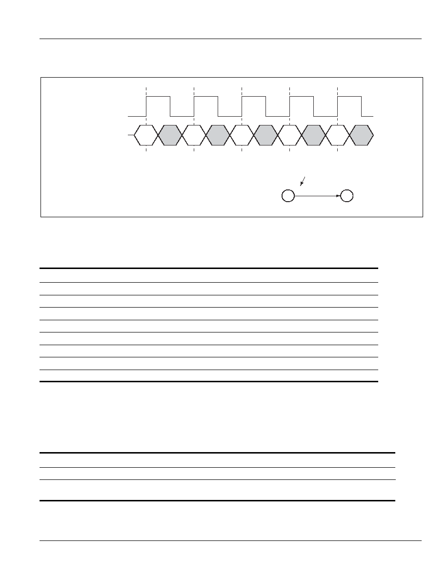
Burst Cycles
RAMs provide an on-chip burst address generator that
can be utilized, if desired, to further simplify burst read or
write implementations. The ADV control pin, when driven
high, commands the
RAM to advance the internal ad-
dress counter and use the counter generated address to
read or write the
RAM. The starting address for the first
cycle in a burst cycle series is loaded into the
RAM by
driving the ADV pin low, into Load mode.
Burst Order
The burst address counter wraps around to its initial state
after four addresses (the loaded address and three more)
have been accessed. SigmaRAMs always count in linear
burst order.
Linear Burst Order
A[1:0]
A[1:0]
A[1:0]
A[1:0]
1st address
00
01
10
11
2nd address
01
10
11
00
3rd address
10
11
00
01
4th address
11
00
01
10
Note:
1. The burst counter wraps to initial state on the 5th rising edge
of clock.
SIGMA PIPELINED BURST READS WITH COUNTER WRAP-AROUND
CLK
A2
Address
E1
W
CQ
DQ
Read
A2
A1
A3
A0
Internal
Address
A3
A2
XX
XX
XX
XX
XX
ADV
Continue
Bursting
10
11
00
01
QA2
QA3
QA0
QA1
Counter Wraps
Continue
Bursting
Continue
Bursting
Continue
Bursting
Continue
Bursting

10
Integrated Silicon Solution, Inc. -- www.issi.com --
1-800-379-4774
ADVANCE INFORMATION
Rev. 00B
11/11/02
IS61LSCS25672
IS61LSCS51236
ISSI
Æ
ECHO CLOCK CONTROL IN TWO BANKS OF SIGMA PIPELINED SRAMS
ECHO CLOCK
RAMs feature Echo Clocks, CQ1, CQ2,
CQ1
, and
CQ2
that track the performance of the output drivers. The Echo
Clocks are delayed copies of the main RAM clock, CLK.
Echo Clocks are designed to track changes in output
driver delays due to variance in die temperature and
supply voltage. The Echo Clocks are designed to fire with
the rest of the data output drivers. Sigma RAMs provide
both in-phase, or true, Echo Clock outputs (CQ1 and
CQ2) and inverted Echo Clock outputs (
CQ1
and
CQ2
).
It should be noted that deselection of the RAM via E2 and
E3 also deselects the Echo Clock output drivers. The
deselection of Echo Clock drivers is always pipelined to
the same degree as output data. Deselection of the RAM via
E1
does not deactivate the Echo Clocks.
In some applications it may be appropriate to pause
between banks; to deselect both RAMs with E1 before
resuming read operations. An E1 deselect at a bank
switch will allow at least one clock to be issued from the
new bank before the first read cycle in the bank. Although
the following drawing illustrates a E1 read pause upon
switching from Bank 1 to Bank 2, a write to Bank 2 would
have the same effect, causing the RAM in Bank 2 to issue
at least one clock before it is needed.
A B C D E F
QA QC
QB QD
Read Read Read Read Read Read
CLK
Address
E1
E2
Bank 1
E2 Bank 2
DQ Bank 1
DQ Bank 2
CQ Bank 1
CQ Bank 2
CQ1+ CQ2
Note:
E1 does not deselect the Echo Clock Outputs. Echo Clock outputs are synchronously deselected by E2 or E3 being sampled false.

Integrated Silicon Solution, Inc. -- www.issi.com --
1-800-379-4774
11
ADVANCE INFORMATION
Rev. 00B
11/11/02
IS61LSCS25672
IS61LSCS51236
ISSI
Æ
PIPELINED READ BANK SWITCH WITH E1 DESELECT
A XX C D E F
QA
QC QD
Read No
Op Read Read Read Read
CLK
Address
E1
E2
Bank 1
E2 Bank 2
DQ Bank 1
DQ Bank 2
CQ Bank 1
CQ Bank 2
CQ1+ CQ2
Note:
E1
does not deselect the Echo Clock Outputs. Echo Clock outputs are synchronously deselected by E2 or E3 being sampled false.
OUTPUT DRIVER IMPEDANCE CONTROL
SigmaRAMs may be supplied with either selectable (high) impedance output drivers. The ZQ pin of SigmaRAMs supplied
with selectable impedance drivers, allows selection between
RAM nominal drive strength (ZQ low) for multi-drop bus
applications and low drive strength (ZQ floating or high) point-to-point applications. The impedance of the data and clock
output drivers in these devices can be controlled via the static input ZQ. When ZQ is tied "low", output driver impedance
is set to ~25
. When ZQ is tied "high" or left unconnected, output driver impedance is set to ~50
.
See the DC Electrical
Characteristics section for further information. The SRAM requires 32K cycles of power-up time after V
DD
reaches its
operating range.
OUTPUT DRIVER CHARACTERISTICS -
TBD
12
Integrated Silicon Solution, Inc. -- www.issi.com --
1-800-379-4774
ADVANCE INFORMATION
Rev. 00B
11/11/02
IS61LSCS25672
IS61LSCS51236
ISSI
Æ
PROGRAMMABLE ENABLES
SRAMs feature two user-programmable chip enable inputs,
E2 and E3. The sense of the inputs, whether they function
as active low or active high inputs, is determined by the
state of the programming inputs, EP2 and EP3. For
example, if EP2 is held at V
DD
, E2 functions as an active
high enable. If EP2 is held to GND , E2 functions as an
active low chip enable input.
BANK ENABLE TRUTH TABLE
EP2
EP3
E2
E3
Bank 0
GND
GND
Active Low
Active Low
Bank 1
GND
V
DD
Active Low
Active High
Bank 2
V
DD
GND
Active High
Active Low
Bank 3
V
DD
V
DD
Active High
Active High
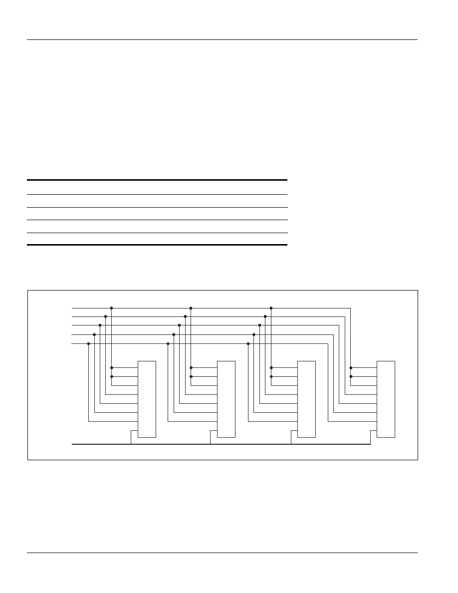
EXAMPLE FOUR BANK DEPTH EXPANSION SCHEMATIC
Programmability of E2 and E3 allows four banks of depth
expansion to be accomplished with no additional logic. By
programming the enable inputs of four SRAMs in binary
sequence (00, 01, 10, 11) and driving the enable inputs
with two address inputs, four SRAMs can be made to look
like one larger RAM to the system.
A
E3
E2
E1
CLK
W
DQ
CQ
A
E3
E2
E1
CLK
W
DQ
CQ
A
0
-A
n-2
A
n-1
A
n
A
E3
E2
E1
CLK
W
DQ
CQ
A
E3
E2
E1
CLK
W
DQ
CQ
A
0
-A
n-2
A
n-1
A
n
A
E3
E2
E1
CLK
W
DQ
CQ
A
E3
E2
E1
CLK
W
DQ
CQ
A
0
-A
n-2
A
n-1
A
n
A
E3
E2
E1
CLK
W
DQ
CQ
A
E3
E2
E1
CLK
W
DQ
CQ
A
0
-A
n-2
A
n-1
A
n
Bank 0
Bank 1
Bank 2
Bank 3
A0-An
E1
CLK
W
DQ0-DQn
CQ

Integrated Silicon Solution, Inc. -- www.issi.com --
1-800-379-4774
13
ADVANCE INFORMATION
Rev. 00B
11/11/02
IS61LSCS25672
IS61LSCS51236
ISSI
Æ
SYNCHRONOUS TRUTH TABLE
CLK
E1
E1
E1
E1
E1
E
ADV
W
W
W
W
W
BW
BW
BW
BW
BW
Previous
Current Operation
DQ/CQ
DQ/CQ
(tn)
(tn)
(tn)
(tn)
(tn)
Operation
(tn)
(tn+1)
0
1
X
F
0
X
X
X
Bank Deselect
***
Hi-Z
0
1
X
X
1
X
X
Bank Deselect
Bank Deselect (Continue)
Hi-Z
Hi-Z
0
1
1
T
0
X
X
X
Deselect
***
Hi-Z/CQ
0
1
X
X
1
X
X
Deselect
Deselect (Continue)
Hi-Z/CQ
Hi-Z/CQ
0
1
0
T
0
0
T
X
Write
***
Dn/CQ
Loads new address
(tn)
Stores DQx if
BWx
= 0
0
1
0
T
0
0
F
X
Write (Abort)
***
Hi-Z/CQ
Loads new address
No data stored
0
1
X
X
1
X
T
Write
Write Continue
Dn-1/CQ
Dn/CQ
Increments address by 1
(tn-1)
(tn)
Stores DQx if
BWx
= 0
0
1
X
X
1
X
F
Write
Write Continue (Abort)
Dn-1/CQ
Hi-Z/CQ
Increments address by 1
(tn-1)
No data stored
0
1
0
T
0
1
X
X
Read
***
Qn/CQ
Loads new address
(tn)
0
1
X
X
1
X
X
Read
Read Continue
Qn-1/CQ
Qn/CQ
Increments address by 1
(tn-1)
(tn)
Notes:
1. If E2 = EP2 and E3 = EP3 then E = "T" else E = "F".
2. If one or more
BWx
= 0 then BW = "T" else BW = "F".
3. "1" = input "high"; "0" = input "low"; "X" = input "don't care"; "T" = input "true"; "F" = input "false".
4. "***" indicates that the DQ input requirement/output state and CQ output state are determined by the previous operation.
5. DQs are tri-stated in response to Bank Deselect, Deselect, and Write commands, one full cycle after the command is sampled.
6. CQs are tri-stated in response to Bank Deselect commands only, one full cycle after the command is sampled.
7. Up to 3 Continue operations may be initiated after initiating a Read or Write operation to burst transfer up to 4 distinct pieces of data per single
external address input. If a fourth (4th) Continue operation is initiated, the internal address wraps back to the initial external (base) address.

14
Integrated Silicon Solution, Inc. -- www.issi.com --
1-800-379-4774
ADVANCE INFORMATION
Rev. 00B
11/11/02
IS61LSCS25672
IS61LSCS51236
ISSI
Æ
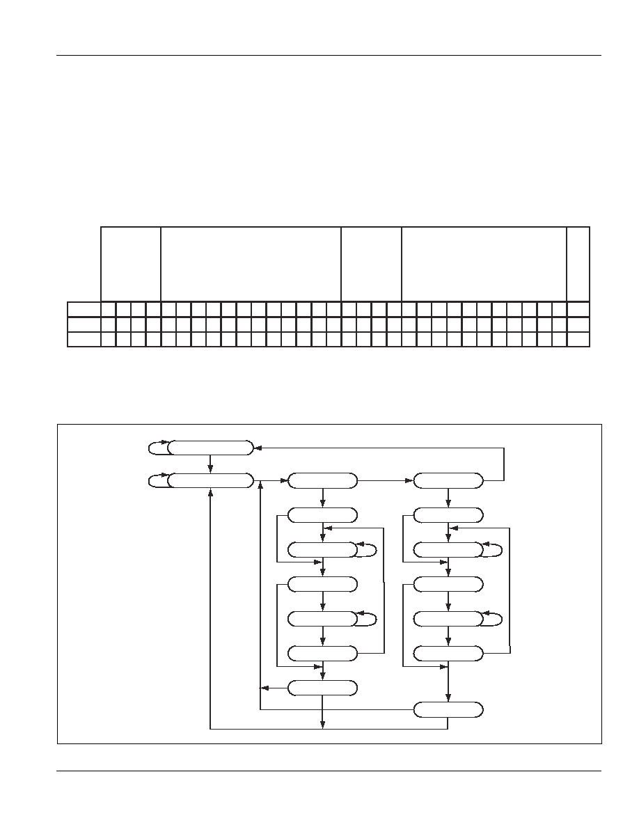
READ/WRITE CONTROL STATE DIAGRAM
READ
READ
CONTINUE
WRITE
WRITE
CONTINUE
DESELECT
BANK
DESELECT
X,F,0,X or
X,X,1,X
1,T,0,X or
X,X,1,X
0,T,0,1
X,X,1,X
X,X,1,X
X,F,0,X
0,T,0,0
X,F,0,X
X,F,0,X
X,F,0,X
0,T,0,0
0,T,0,0
0,T,0,0
0,T,0,0
0,T,0,1
0,T,0,0
0,T,0,1
0,T,0,1
0,T,0,1
1,T,0,X
1,T,0,X
1,T,0,X
1,T,0,X
1,T,0,X
X,X,1,X
X,X,1,X
0,T,0,1
X,F,0,X
Notes:
1. The notation "X,X,X,X" controlling the state transitions above indicate the states of inputs
E1
, E, ADV, and
W
respectively.
2. If (E2 = EP2 and E3 = EP3) then E = "T" else E = "F".
3. "1" = input "high"; "0" = input "low"; "X" = input "don't care"; "T" = input "true"; "F" = input "false".
Integrated Silicon Solution, Inc. -- www.issi.com --
1-800-379-4774
15
ADVANCE INFORMATION
Rev. 00B
11/11/02
IS61LSCS25672
IS61LSCS51236
ISSI
Æ
ABSOLUTE MAXIMUM RATINGS
(All voltages reference to GND )
Symbol
Description
Value
Unit
V
DD
Voltage on V
DD
Pins
≠0.5 to 2.5
V
V
DDQ
Voltage in V
DDQ
Pins
≠0.5 to 2.3
V
V
I/O
Voltage on I/O Pins
≠0.5 to V
DDQ
+0.5 (
2.3 V max.)
V
V
IN
Voltage on Other Input Pins
≠0.5 to V
DDQ
+0.5 (
2.3 V max.)
V
I
IN
Input Current on Any Pin
±100
mA dc
I
OUT
Output Current on Any Pin
±100
mA dc
T
J
Maximum Junction Temperature
125
∞
C
T
STG
Storage Temperature
-55 to 125
∞
C
Note:
Permanent device damage may occur if Absolute Maximum Ratings are exceeded. Operation should be limited to Recommended
Operating Conditions. Exposure to conditions exceeding Recommended Operating Conditions, for an extended period of time, may
affect reliability of this component.
CURRENT STATE & NEXT STATE DEFINITION FOR READ/WRITE CONTROL STATE DIAGRAM
n n+1
n+2
n+3
Current State
Next State
CK
Command
Transition
Current State (n)
Input Command Code
Next State (n+1)
KEY
POWER SUPPLY CHARACTERISTICS
(T
A
= 0 min., 25 typ, 70 max ∞C)
Symbol
Parameter
Min.
Typ.
Max.
Unit
V
DD
Supply Voltage
1.7
1.8
1.9
V
V
DDQ
(1)
1.8 V I/O Supply Voltage
1.7
1.8
V
DD
V
1.5 V I/O Supply Voltage
1.4
1.5
1.6
V
Note:
1. Unless otherwise noted, all performance specifications quoted are evaluated for worst case at both 1.4 V
V
DDQ
1.6V
(i.e., 1.5 V I/O) and 1.7 V
V
DDQ
1.95 V (i.e., 1.8 V I/O) and quoted at whichever condition is worst case.
16
Integrated Silicon Solution, Inc. -- www.issi.com --
1-800-379-4774
ADVANCE INFORMATION
Rev. 00B
11/11/02
IS61LSCS25672
IS61LSCS51236
ISSI
Æ
CMOS I/O DC INPUT CHARACTERISTICS
Symbol
Parameter
V
DDQ
Min.
Typ.
Max.
Unit
V
IH
CMOS Input High Voltage
1.8
1.2
--
V
DDQ
+ 0.3
V
1.5
1.0
--
V
DDQ
+ 0.3
V
IL
CMOS Input Low Voltage
1.8
≠0.3
--
0.6
V
1.5
≠0.3
--
0.5
Note:
For devices supplied with CMOS input buffers. Compatible with both 1.8 V and 1.5 V I/O drivers.
I/O CAPACITANCE (T
A
= 25 ∞C, f = 1 MH
Z
)
Symbol
Parameter
Test conditions
Min.
Max.
Unit
C
A
Address
Input Capacitance
V
IN
= 0 V
--
3.5
pF
C
B
Control
Input Capacitance
V
IN
= 0 V
--
3.5
pF
C
CK
Clock
Input Capacitance
V
IN
= 0 V
--
3.5
pF
C
DQ
Data
Output Capacitance
V
OUT
= 0 V
--
4.5
pF
C
CQ
CQ Clock
Output Capacitance
V
OUT
= 0 V
--
4.5
pF
Note: These parameters are sampled and not 100% tested.
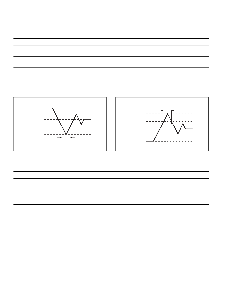
Undershoot Measurement and Timing
Overshoot Measurement and Timing
20% t
KC
50%
GND
V
IH
GND - 1.0V
20% t
KC
50%
V
DD
+ 1.0V
V
DD
V
IL
Integrated Silicon Solution, Inc. -- www.issi.com --
1-800-379-4774
17
ADVANCE INFORMATION
Rev. 00B
11/11/02
IS61LSCS25672
IS61LSCS51236
ISSI
Æ
AC TEST CONDITIONS
(V
DD
= 1.8V ± 0.1V, T
A
= 0 to 85∞C)
Parameter
Symbol
Conditions
Units
V
DDQ
1.5V±0.1
1.8 ±0.1
V
Input High Level
V
IH
1.25
1.4
V
Input Low Level
V
IL
0.25
0.4
V
Input Rise & Fall Time
2.0
2.0
V/ns
Input Reference Level
0.75
0.9
V
Clock Input High Voltage
V
KIH
1.25
1.4
V
Clock Input Low Voltage
V
KIL
0.25
0.4
V
Clock Input Rise & Fall Time
2.0
2.0
V/ns
Clock Input Reference Level
0.75
0.9
V
Output Reference Level
0.75
0.9
V
Output Load Conditions ZQ = V
IH
see below
see below
Notes:
1. Include scope and jig capacitance.
2. Test conditions as specified with output loading as shown unless otherwise noted.
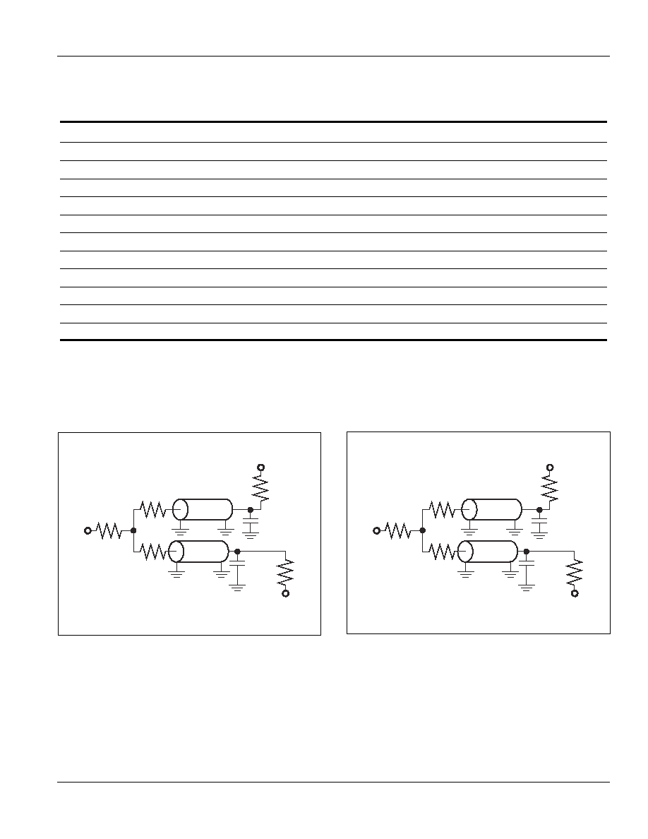
AC TEST LOADS
DQ
0.75V
50
50
16.7
16.7
50
16.7
0.75V
50
5 pF
5 pF
V
DDQ
= 1.5V
DQ
0.9V
50
50
16.7
16.7
50
16.7
0.9V
50
5 pF
5 pF
V
DDQ
= 1.8V
Figure 1 (V
DDQ
= 1.5V)
Figure 2 (V
DDQ
= 1.8V)

18
Integrated Silicon Solution, Inc. -- www.issi.com --
1-800-379-4774
ADVANCE INFORMATION
Rev. 00B
11/11/02
IS61LSCS25672
IS61LSCS51236
ISSI
Æ
SELECTABLE IMPEDANCE OUTPUT DRIVER DC ELECTRICAL CHARACTERISTICS
Symbol
Parameter
Test Conditions
Min.
Max.
Units
V
OHL
(1)
Low Drive Output High Voltage
I
OHL
= ≠4 mA
V
DDQ
≠ 0.4
--
V
V
OLL
(1)
Low Drive Output Low Voltage
I
OLL
= 4 mA
--
0.4
V
V
OHH
(2)
High Drive Output High Voltage
I
OHH
= ≠8 mA
V
DDQ
≠ 0.4
--
V
V
OLH
(2)
High Drive Output Low Voltage
I
OLH
= 8 mA
--
0.4
V
Notes:
1. ZQ = 1; High Impedance output driver setting
2. ZQ = 0; Low Impedance output driver setting
OUTPUT RESISTANCE
Symbol
Parameter
Test Conditions
Min.
Typ.
Max.
Units
R
OUT
Output Resistance
V
OH
,
V
OL
= V
DDQ
/2
17
25
33
ZQ = V
IL
V
OH
,
V
OL
= V
DDQ
/2
35
50
65
ZQ = V
IH

Integrated Silicon Solution, Inc. -- www.issi.com --
1-800-379-4774
19
ADVANCE INFORMATION
Rev. 00B
11/11/02
IS61LSCS25672
IS61LSCS51236
ISSI
Æ
DC ELECTRICAL CHARACTERISTICS
(V
DD
= 1.8V ±0.1V, GND = 0V, T
A
= 0
∞
to 85
∞
C)
Symbol
Parameter
Test Conditions
Min
Typ
Max
Units
I
LI
Input Leakage Current
V
IN
= GND to V
DDQ
-5
--
5
uA
(Address, Control, Clock)
I
MLI
Input Leakage Current
V
MIN
= GND to V
DD
-10
--
10
uA
(EP2, EP3, M2, M3, M4, ZQ)
I
DLI
Input Leakage Current
V
DIN
= GND to V
DDQ
-10
--
10
uA
(Data)
OPERATING CURRENTS
Symbol
Parameter
Test Conditions
-333
-300
-250
Units
Com. Ind.
Com. Ind.
Com. Ind.
I
CC
Operating Current
E1 < V
IL
Max.
Pipeline x72
650
mA
t
KHKH
> t
KHKH
Min.
x36
550
All other inputs
V
IL
> V
IN
> V
IH
I
SB
1
Bank Deselect Current
E1 < V
IH
Min. or
Pipeline x72
250
mA
&
&
E2 or E3 False
x36
225
I
SB
2
Chip Disable Current
t
KHKH
> t
KHKH
Min.
All other inputs
V
IL
> V
IN
> V
IH
I
SB
3
CMOS Deselect Current
Device Deselected
Pipeline x72
150
mA
All inputs
x36
150
GND+0.10V > V
IN
> V
DD
≠0.10V
Note: Com. = 0∞C to 70∞C
Ind. = ≠40∞C to +85∞C

20
Integrated Silicon Solution, Inc. -- www.issi.com --
1-800-379-4774
ADVANCE INFORMATION
Rev. 00B
11/11/02
IS61LSCS25672
IS61LSCS51236
ISSI
Æ
AC ELECTRICAL CHARACTERISTICS
-333
-300
-250
Symbol
Parameter
Min
Max
Min
Max
Min
Max
Unit
t
KHKH
Clock Cycle Time
3.0
--
3.3
--
4.0
--
ns
t
KHKL
Clock HIGH Time
1.2
--
1.3
--
1.5
--
ns
t
KLKH
Clock LOW Time
1.2
--
1.3
--
1.5
--
ns
t
KHCX
1
(2)
Clock High to Echo Clock Low-Z
0.5
--
0.5
--
0.5
--
ns
t
KHCH
Clock High to Echo Clock High
0.5
1.5
0.5
1.7
0.5
2.0
ns
t
CHCL
(2)
Echo Clock High Time
t
KHKL
±200 ps
t
KHKL
±200 ps
t
KHKL
±250 ps
ns
t
KLCL
Clock Low to Echo Clock Low
0.5
1.5
0.5
1.7
0.5
2.0
ns
t
CLCH
(2)
Echo Clock Low Time
t
KLKH
±200 ps
t
KLKH
±200 ps
t
KLKH
±250 ps
ns
t
KHCZ
(1, 2)
Clock High to Echo Clock High-Z
--
1.5
--
1.7
--
2.0
ns
t
KHQX
1
(1)
Clock High to Output in Low-Z
0.5
--
0.5
--
0.5
--
ns
t
KHQV
Clock High to Output Valid
--
1.6
--
1.8
--
2.1
ns
t
KHQX
Clock High to Output Invalid
0.5
--
0.5
--
0.5
--
ns
t
KHQZ
(1)
Clock High to Output in High-Z
0.5
1.6
0.5
1.8
0.5
2.1
ns
t
CHQV
(2)
Echo Clock High to Output Valid
--
0.4
--
0.4
--
0.5
ns
t
CHQX
(2)
Output Invalid to Echo Clock High
--
≠0.4
--
≠0.4
--
≠0.5
ns
t
AVKH
Address Valid to Clock High
0.6
--
0.7
--
0.8
--
ns
t
KHAX
Clock High to Address Don't Care
0.4
--
0.4
--
0.5
--
ns
t
EVKH
Enable Valid to Clock High
0.6
--
0.7
--
0.8
--
ns
t
KHEX
Clock High to Enable Don't Care
0.4
--
0.4
--
0.5
--
ns
t
WVKH
Write Valid to Clock High
0.6
--
0.7
--
0.8
--
ns
t
KHWX
Clock High to Write Don't Care
0.4
--
0.4
--
0.5
--
ns
t
BVKH
Byte Write Valid to Clock High
0.6
--
0.7
--
0.8
--
ns
t
KHBX
Clock High to Byte Write Don't Care
0.4
--
0.4
--
0.5
--
ns
t
DVKH
Data In Valid to Clock High
0.6
--
0.7
--
0.8
--
ns
t
KHDX
Clock High to Data In Don't Care
0.4
--
0.4
--
0.5
--
ns
t
advVKH
ADV Valid to Clock High
0.6
--
0.7
--
0.8
--
ns
t
KHadvX
Clock High to ADV Don't Care
0.4
--
0.4
--
0.5
--
ns
Notes:
1. Measured at 100 mV from steady state. Not 100% tested.
2. Guaranteed by design. Not 100% tested.
3. For any specific temperature and voltage t
KHCZ
< t
KHCX
1.

Integrated Silicon Solution, Inc. -- www.issi.com --
1-800-379-4774
21
ADVANCE INFORMATION
Rev. 00B
11/11/02
IS61LSCS25672
IS61LSCS51236
ISSI
Æ
AC ELECTRICAL CHARACTERISTICS
-225
-200
Symbol
Parameter
Min
Max
Min
Max
Unit
t
KHKH
Clock Cycle Time
4.5
--
5.0
--
ns
t
KHKL
Clock HIGH Time
1.8
--
2.0
--
ns
t
KLKH
Clock LOW Time
1.8
--
2.0
--
ns
t
KHCX
1
(2)
Clock High to Echo Clock Low-Z
0.5
--
0.5
--
ns
t
KHCH
Clock High to Echo Clock High
0.5
2.5
0.5
3.0
ns
t
CHCL
(2)
Echo Clock High Time
t
KHKL
±250 ps t
KHKL
±250 ps ns
t
KLCL
Clock Low to Echo Clock Low
0.5
2.5
0.5
3.0
ns
t
CLCH
(2)
Echo Clock Low Time
t
KLKH
±200 ps t
KLKH
±200 ps ns
t
KHCZ
(1, 2)
Clock High to Echo Clock High-Z
--
2.5
--
3.0
ns
t
KHQX
1
(1)
Clock High to Output in Low-Z
0.5
--
0.5
--
ns
t
KHQV
Clock High to Output Valid
--
2.6
--
3.1
ns
t
KHQX
Clock High to Output Invalid
0.5
--
0.5
--
ns
t
KHQZ
(1)
Clock High to Output in High-Z
0.5
2.6
0.5
3.1
ns
t
CHQV
(2)
Echo Clock High to Output Valid
--
0.5
-- 0.5 ns
t
CHQX
(2)
Output Invalid to Echo Clock High
--
≠0.5
--
≠0.5
ns
t
AVKH
Address Valid to Clock High
1.1
--
1.5
--
ns
t
KHAX
Clock High to Address Don't Care
0.5
--
0.5
--
ns
t
EVKH
Enable Valid to Clock High
1.1
--
1.5
--
ns
t
KHEX
Clock High to Enable Don't Care
0.5
--
0.5
--
ns
t
WVKH
Write Valid to Clock High
1.1
--
1.5
--
ns
t
KHWX
Clock High to Write Don't Care
0.5
--
0.5
--
ns
t
BVKH
Byte Write Valid to Clock High
1.1
--
1.5
--
ns
t
KHBX
Clock High to Byte Write Don't Care
0.5
--
0.5
--
ns
t
DVKH
Data In Valid to Clock High
1.1
--
1.5
--
ns
t
KHDX
Clock High to Data In Don't Care
0.5
--
0.5
--
ns
t
advVKH
ADV Valid to Clock High
1.1
--
1.5
--
ns
t
KHadvX
Clock High to ADV Don't Care
0.5
--
0.5
--
ns
Notes:
1. Measured at 100 mV from steady state. Not 100% tested.
2. Guaranteed by design. Not 100% tested.
3. For any specific temperature and voltage t
KHCZ
< t
KHCX
1.
22
Integrated Silicon Solution, Inc. -- www.issi.com --
1-800-379-4774
ADVANCE INFORMATION
Rev. 00B
11/11/02
IS61LSCS25672
IS61LSCS51236
ISSI
Æ
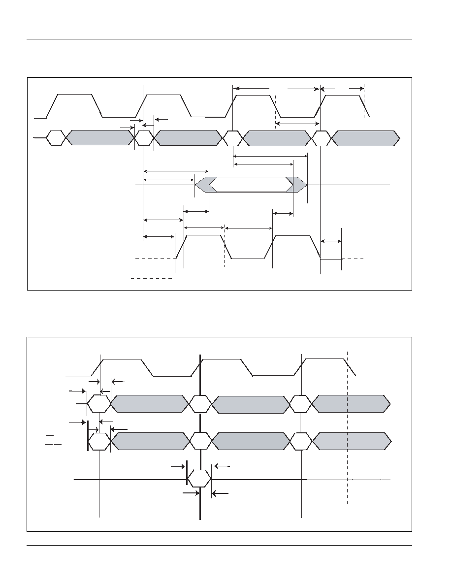
TIMING PARAMETER KEY--PIPELINED READ CYCLE TIMING
TIMING PARAMETER KEY--LATE WRITE MODE CONTROL AND DATA IN TIMING
Note: tn
VKH
= t
EVKH
, t
WVKH
, t
BVKH
, etc. and t
KH
n
X
= t
KHEX
, t
KHWX
, t
KHBX
, etc.
QB
t
KLKH
t
KHKH
t
KHKL
t
KHQZ
t
KHQX
t
KHQV
t
KHQX1
t
CQHQV
t
KHCQH
t
KHCQX1
t
CQHCQL
t
CQLCQH
t
CQHQX
t
KHCQZ
= CQ High Z
t
KHAX
t
AVKH
C
D
E
CK
DQ
CQ
B
A
B
C
CK
ADDRESS
E1,E2,E3
W, Bn, ADV
t
AVKH
t
KHAX
t
n
VKH
t
KH
n
X
DQ
DA
t
DVKH
t
KHDX
Control
"A"

Integrated Silicon Solution, Inc. -- www.issi.com --
1-800-379-4774
23
ADVANCE INFORMATION
Rev. 00B
11/11/02
IS61LSCS25672
IS61LSCS51236
ISSI
Æ
JTAG PORT OPERATION
Overview
These devices provide a JTAG Test Access Port (TAP) and
Boundary Scan interface using a limited set of IEEE std.
1149.1 functions. This test mode is intended to provide a
mechanism for testing the interconnect between master
(processor, controller, etc.), SRAMs, other components,
and the printed circuit board.
In conformance with a subset of IEEE std. 1149.1, these
devices contain a TAP Controller and four TAP Registers.
The TAP Registers consist of one Instruction Register
JTAG PIN DESCRIPTIONS
Pin
Pin Name
I/O
Description
TCK
Test Clock
In
Clocks all TAP events. All inputs are captured on the rising edge of TCK and
all outputs propagate from the falling edge of TCK.
TMS
Test Mode Select
In
The TMS input is sampled on the rising edge of TCK. This is the command input
for the TAP controller. An undriven TMS input will produce the same result as
a logic one input level.
TDI
Test Data In
In
The TDI input is sampled on the rising edge of TCK. This is the input side of the
serial registers placed between TDI and TDO. The register placed between TDI
and TDO is determined by the state of the TAP Controller and the instruction
that is currently loaded in the TAP Instruction Register (refer to the TAP
Controller State Diagram). An undriven TDI pin will produce the same result as
a logic one input level.
TDO
Test Data Out
Out
Output that is active depending on the state of the TAP Controller. Output
changes in response to the falling edge of TCK. This is the output side of the
serial registers placed between TDI and TDO.
Note:
This device does not have a TRST (TAP Reset) pin. TRST is optional in IEEE 1149.1. The Test-Logic-Reset state is entered while
TMS is held high for five rising edges of TCK. The TAP Controller is also reset automatically at power-up.
and three Data Registers (ID, Bypass, and Boundary
Scan Registers).
Disabling the JTAG Port
It is possible to use this device without utilizing the JTAG
port. The port is reset at power-up and will remain inactive
unless clocked. To assure normal operation of the RAM
with the JTAG Port unused, TCK should be tied Low, TDI
and TMS may be left floating or tied to V
DD
. TDO should be
left unconnected.

24
Integrated Silicon Solution, Inc. -- www.issi.com --
1-800-379-4774
ADVANCE INFORMATION
Rev. 00B
11/11/02
IS61LSCS25672
IS61LSCS51236
ISSI
Æ
JTAG TAP BLOCK DIAGRAM
Bypass Register
Instruction Register
ID Code Register
Boundary Scan Register
. . .
. . . . .
0
2 1 0
31 30 29
2 1 0
n
2 1 0
Test Access Port (TAP) Controller
TDI
TMS
TCK
TDO
JTAG PORT REGISTERS
Overview
The JTAG registers, referred to as Test Access Port (TAP)
registers, are selected (one at a time) via the sequences
of 1s and 0s applied to TMS as TCK is strobed. Each of
the TAP registers are serial shift registers that capture
serial input data on the rising edge of TCK and push serial
data out on the next falling edge of TCK. When a register
is selected, it is placed between the TDI and TDO pins.
Instruction Register
The Instruction Register holds the instructions that are
executed by the TAP controller when it is moved into the
Run, Test/Idle, or the various data register states. In-
structions are 3 bits long. The Instruction Register can be
loaded when it is placed between the TDI and TDO pins.
The Instruction Register is automatically preloaded with
the IDCODE instruction at power-up or whenever the
controller is placed in Test-Logic-Reset state.
Bypass Register
The Bypass Register is a single-bit register that can be
placed between TDI and TDO. It allows serial test data to
be passed through the RAM's JTAG Port to another
device in the scan chain with as little delay as possible.
Boundary Scan Register
The Boundary Scan Register is a collection of flip flops that can be
preset by the logic level found on the RAM's input or I/O pins. The
flip flops are then daisy chained together so the levels found can be
shifted serially out of the JTAG Port's TDO pin. The Boundary Scan
Register also includes a number of place holder flip flops (always set
to a logic 1). The relationship between the device pins and the bits
in the Boundary Scan Register is described in the following Scan
Order Table. The Boundary Scan Register, under the control of the
TAP Controller, is loaded with the contents of the RAMs I/O ring
when the controller is in Capture-DR state and then is placed
between the TDI and TDO pins when the controller is moved to
Shift-DR state. SAMPLE-Z, SAMPLE/PRELOAD and EXTEST
instructions can be used to activate the Boundary Scan Register.
Integrated Silicon Solution, Inc. -- www.issi.com --
1-800-379-4774
25
ADVANCE INFORMATION
Rev. 00B
11/11/02
IS61LSCS25672
IS61LSCS51236
ISSI
Æ
JTAG TAP CONTROLLER STATE DIAGRAM
Select DR
Capture DR
Shift DR
Exit1 DR
Pause DR
Exit2 DR
Update DR
Select IR
Capture IR
Shift IR
Exit1 IR
Pause IR
Exit2 IR
Update IR
Test Logic Reset
Run Test Idle
1
1
1
1
1
1
1
1
1
1
1
1
1
1
0
0
0
0
1
0
0
0
0
0
0
0
0
0
0
0
1
0
IDENTIFICATION (ID) REGISTER
The ID Register is a 32-bit register that is loaded with a
device and vendor specific 32-bit code when the controller
is put in Capture-DR state with the IDCODE command
loaded in the Instruction Register. The code is loaded from
a 32-bit on-chip ROM. It describes various attributes of
the RAM as indicated below. The register is then placed
between the TDI and TDO pins when the controller is
moved into Shift-DR state. Bit 0 in the register is the LSB
and the first to reach TDO when shifting begins.
Bit #
31 30 29 28 27 26 25 24 23 22 21 20 19 18 17 16 15 14 13 12 11 10 9
8
7
6
5
4
3
2
1
0
x72
X X X X
0
0
0
0
0
0
0
0 0
0
0
0
1
1
0
0
0
0
0
1
1
0
1
0
1
0
1
1
x36
X X X X 0 0
0 0
0 0
0 0 0
0 0
0 1 0
0 0
0 0 0 1
1
0 1 0
1 0
1
1
Presence Register
Die
I/O
ISSI Technology
Revision
Not Used
Configuration
JEDEC Vendor
Code
ID Code
ID REGISTER CONTENTS

26
Integrated Silicon Solution, Inc. -- www.issi.com --
1-800-379-4774
ADVANCE INFORMATION
Rev. 00B
11/11/02
IS61LSCS25672
IS61LSCS51236
ISSI
Æ
JTAG TAP INSTRUCTION SET SUMMARY
Instruction
Code
Description
EXTEST
(1)
000
Places the Boundary Scan Register between TDI and TDO. When EXTEST is
selected, data will be driven out of the DQ pad.
IDCODE
(1,2)
001
Preloads ID Register and places it between TDI and TDO.
SAMPLE-Z
(1)
010
Captures I/O ring contents. Places the Boundary Scan Register between TDI
and TDO. Forces all Data and Clock output drivers to High-Z.
RFU
(1)
011
Do not use this instruction; Reserved for Future Use. Replicates BYPASS
instruction. Places Bypass Register between TDI and TDO.
SAMPLE/PRELOAD
(1)
100
Captures I/O ring contents. Places the Boundary Scan Register between TDI and TDO.
Private
(1)
101
Private instruction.
RFU
(1)
110
Do not use this instruction; Reserved for Future Use.
BYPASS
(1)
111
Places Bypass Register between TDI and TDO.
Notes:
1. Instruction codes expressed in binary, MSB on left, LSB on right.
2. Default instruction automatically loaded at power-up and in Test-Logic-Reset state.
TAP CONTROLLER INSTRUCTION SET
Overview
There are two classes of instructions defined in the
Standard 1149.1-1990; standard (public) instructions, and
device specific (private) instructions. Some public instructions
are mandatory for 1149.1 compliance. Optional public
instructions must be implemented in prescribed ways.
The TAP on this device may be used to monitor all input
and I/O pads. This device will not perform INTEST but can
preform the preload portion of the SAMPLE/PRELOAD
command.
When the TAP controller is placed in Capture-IR state, the
two least significant bits of the instruction register are
loaded with 01. When the controller is moved to the Shift-IR
state, the Instruction Register is placed between TDI and
TDO. In this state the desired instruction is serially loaded
through the TDI input (while the previous contents are
shifted out at TDO). For all instructions, the TAP executes
newly loaded instructions only when the controller is
moved to Update-IR state. The TAP instruction set for this
device is listed in the JTAG TAP Instruction Set Summary.

Integrated Silicon Solution, Inc. -- www.issi.com --
1-800-379-4774
27
ADVANCE INFORMATION
Rev. 00B
11/11/02
IS61LSCS25672
IS61LSCS51236
ISSI
Æ
JTAG DC RECOMMENDED OPERATING CONDITIONS (T
A
= 0 to 85∞C)
Symbol
Parameter
Test Conditions
Min.
Max.
Unit
V
TIH
JTAG Input High Voltage
1.2
V
DD
+0.3
V
V
TIL
JTAG Input Low Voltage
-0.3
0.6
V
V
TOH
JTAG Output High Voltage
CMOS
I
TOH
= -100
µ
V
DD
-0.1
--
V
TTL
I
TOH
= -8m
V
DD
-0.4
--
V
TOL
JTAG Output Low Voltage
CMOS
I
TOL
= 100
µ
--
0.1
V
TTL
I
TOL
= 8m
--
0.4
I
TLI
JTAG Input Leakage Current
V
TIN
=GND to V
DD
-10
10
µ
JTAG AC TEST CONDITIONS (V
DD
= 1.8V ±0.1V, T
A
= 0 to 85∞C)
Symbol
Parameter
Test Conditions
Unit
V
TIH
JTAG Input High Voltage
1.6
V
V
TIL
JTAG Input Low Voltage
0.2
V
JTAG Input Rise & Fall Time
1.0
V/ns
JTAG Input Reference Level
0.9
V
JTAG Output Reference Level
0.9
V
JTAG Output Load Condition
see AC TEST LOADS

28
Integrated Silicon Solution, Inc. -- www.issi.com --
1-800-379-4774
ADVANCE INFORMATION
Rev. 00B
11/11/02
IS61LSCS25672
IS61LSCS51236
ISSI
Æ
Symbol
Parameter
Min
Max
Unit
t
THTH
TCK Cycle Time
20
--
ns
t
THTL
TCK High Pulse Width
8
--
ns
t
TLTH
TCK Low Pulse Width
8
--
ns
t
MVTH
TMS Setup Time
5
--
ns
t
THMX
TMS Hold Time
5
--
ns
t
DVTH
TDI Set Up Time
5
--
ns
t
THDX
TDI Hold Time
5
--
ns
t
TLQV
TCK Low to TDO Valid
--
10
ns
t
TLQX
TCK Low to TDO Hold
0
--
ns
JTAG PORT TIMING DIAGRAM
TCK
TMS
TDI
TDO
t
THTL
t
TLTH
t
THTH
t
MVTH
t
THMX
t
DVTH
t
THDX
t
TLQX
t
TLQV
JTAG PORT AC ELECTRICAL CHARACTERISTICS

Integrated Silicon Solution, Inc. -- www.issi.com --
1-800-379-4774
29
ADVANCE INFORMATION
Rev. 00B
11/11/02
IS61LSCS25672
IS61LSCS51236
ISSI
Æ
INSTRUCTION DESCRIPTIONS
BYPASS
When the BYPASS instruction is loaded to the Instruction
Register, the Bypass Register is placed between TDI and
TDO. This occurs when the TAP controller is moved to the
Shift-DR state. This allows the board level scan path to be
shortened to facilitate testing of other devices in the scan
path.
SAMPLE/PRELOAD
SAMPLE/PRELOAD is a Standard 1149.1 mandatory public
instruction. When the SAMPLE/PRELOAD instruction is
loaded in the Instruction Register, moving the TAP controller
into the Capture-DR state loads the data in the RAMs input
and I/O buffers into the Boundary Scan Register. Some
Boundary Scan Register locations are not associated with
an input or I/O pin, and are loaded with the default state
identified in the BSDL file. Because the RAM clock is
independent from the TAP Clock (TCK) it is possible for
the TAP to attempt to capture the I/O ring contents while
the input buffers are in transition (i.e. in a metastable
state). Although allowing the TAP to sample metastable
inputs will not harm the device, repeatable results cannot
be expected. RAM input signals must be stabilized for
long enough to meet the TAP's input data capture set-up
plus hold time (t
TS
plus t
TH
). The RAM's clock inputs need
not be paused for any other TAP operation except captur-
ing the I/O ring contents into the Boundary Scan Register.
Moving the controller to Shift-DR state then places the
Boundary Scan Register between the TDI and TDO pins.
EXTEST
EXTEST is an IEEE 1149.1 mandatory public instruction.
It is to be executed whenever the instruction register is
loaded with all logic 0s. The EXTEST command does not
block or override the RAM's input pins; therefore, the
RAM's internal state is still determined by its input pins.
Typically, the Boundary Scan Register is loaded with the
desired pattern of data with the SAMPLE/PRELOAD
command. Then the EXTEST command is used to output
the Boundary Scan Register's contents, in parallel, on the
RAM's data output drivers on the falling edge of TCK when
the controller is in the Update-IR state.
Alternately, the Boundary Scan Register may be loaded in
parallel using the EXTEST command. When the EXTEST
instruction is selected, the state of all the RAM's input and
I/O pins, as well as the default values at Scan Register
locations not associated with a pin (pin marked NC), are
transferred in parallel into the Boundary Scan Register on
the rising edge of TCK in the Capture-DR state, the RAM's
output pins drive out the value of the Boundary Scan
Register location with which each output pin is associated.
IDCODE
The IDCODE instruction causes the ID ROM to be loaded
to the ID register when the controller is in Capture-DR
mode and places the ID register between the TDI and TDO
pins in Shift-DR mode. The IDCODE instruction is the
default instruction loaded in at power up and any time the
controller is placed in the Test-Logic-Reset state.
SAMPLE-Z
If the SAMPLE-Z instruction is loaded to the instruction
register, all RAM outputs are forced to inactive state
(high-Z) and the Boundary Scan Register is connected
between TDI and TDO when the TAP controller is moved
to the Shift-DR state.
RFU
These instructions are reserved for future use. In this
device they replicate the BYPASS instruction.

30
Integrated Silicon Solution, Inc. -- www.issi.com --
1-800-379-4774
ADVANCE INFORMATION
Rev. 00B
11/11/02
IS61LSCS25672
IS61LSCS51236
ISSI
Æ
BOUNDARY SCAN ORDER ASSIGNMENTS (by Exit Sequence) -
PH=Place Holder
X72
Ball Loc.
X36
Sequence
Pkg. Ball
Sequence
Pkg. Ball
1
A0
W6
1
A0
2
A
V7
2
A
3
A
V8
3
A
4
A
U 8
4
A
5
A
V9
5
A
6
A
U 6
6
A
7
PH
(1)
U 5
7
PH
(1)
8
A
W7
8
A
9
PH
(1)
U 7
9
PH
(1)
10
MCL
T6
10
MCL
11
M3
M6
11
M3
12
M4
J6
12
M4
13
MCL
K6
13
MCL
14
MCL
D 6
14
MCL
15
PH
(1)
C 7
15
PH
(1)
16
Be
C 8
17
Ba
C 9
16
Ba
18
Bb
B8
17
Bb
19
Bf
B9
20
W
B6
18
W
21
ADV
A6
19
ADV
22
A
B7
20
A
23
E3
A8
21
E3
24
A
A9
22
A
25
ZQ
F6
23
ZQ
26
A
A3
24
A
27
E2
A4
25
E2
28
A
A5
26
A
29
A
A7
27
A
B5
28
AO36
30
Bc
B3
29
Bc
31
Bg
B4
32
Bh
C 3
33
Bd
C 4
30
Bd
34
PH
(1)
C 5
31
PH
(1)
35
E1
C 6
32
E1
36
EP2
G6
33
EP2
37
EP3
H 6
34
EP3
38
CK
K3
35
CK
39
M2
L6
36
M2
Note:
1. Input of PH register connected to Vss.

Integrated Silicon Solution, Inc. -- www.issi.com --
1-800-379-4774
31
ADVANCE INFORMATION
Rev. 00B
11/11/02
IS61LSCS25672
IS61LSCS51236
ISSI
Æ
BOUNDARY SCAN ORDER ASSIGNMENTS (by Exit Sequence) Continued:
X72
Ball Loc.
X36
Sequence
Pkg. Ball
Sequence
Pkg. Ball
40
MCH
N 6
37
MCH
41
MCL
P6
38
MCL
42
A
V3
39
A
43
A
U 4
40
A
44
A
V4
41
A
45
A
V5
42
A
46
A
W5
43
A
47
A
V6
44
A
48
DQd
W2
45
DQd
49
DQd
W1
46
DQd
50
DQd
V2
47
DQd
51
DQd
V1
48
DQd
52
DQd
U 2
49
DQd
53
DQd
U 1
50
DQd
54
DQd
T2
51
DQd
55
DQd
T1
52
DQd
56
DQPd
R 1
53
DQPd
57
DQPh
R 2
58
DQh
P2
59
DQh
P1
60
DQh
N 2
61
DQh
N 1
62
DQh
M2
63
DQh
M1
64
DQh
L2
65
DQh
L1
66
CQ2
K2
54
CQ2
67
CQ2
K1
55
CQ2
68
DQc
J2
56
DQc
69
DQc
J1
57
DQc
70
DQc
H 2
58
DQc
71
DQc
H 1
59
DQc
72
DQc
G2
60
DQc
73
DQc
G1
61
DQc
74
DQc
F2
62
DQc
75
DQc
F1
63
DQc
76
DQPc
E2
64
DQPc
77
DQPg
E1
78
DQg
D 2
79
DQg
D 1
80
DQg
C 2
81
DQg
C 1

32
Integrated Silicon Solution, Inc. -- www.issi.com --
1-800-379-4774
ADVANCE INFORMATION
Rev. 00B
11/11/02
IS61LSCS25672
IS61LSCS51236
ISSI
Æ
BOUNDARY SCAN ORDER ASSIGNMENTS (by Exit Sequence) Continued:
X72
Ball Loc.
X36
Sequence
Pkg. Ball
Sequence
Pkg. Ball
82
DQg
B2
83
DQg
B1
84
DQg
A2
85
DQg
A1
86
DQb
A10
65
DQb
87
DQb
A11
66
DQb
88
DQb
B10
67
DQb
89
DQb
B11
68
DQb
90
DQb
C10
69
DQb
91
DQb
C11
70
DQb
92
DQb
D10
71
DQb
93
DQb
D11
72
DQb
94
DQPb
E11
73
DQPb
95
DQPf
E10
96
DQf
F10
97
DQf
F11
98
DQf
G10
99
DQf
G11
100
DQf
H10
101
DQf
H11
102
DQf
J10
103
DQf
J11
104
CQ1
K11
74
CQ1
105
CQ1
K10
75
CQ1
106
DQa
L10
76
DQa
107
DQa
L11
77
DQa
108
DQa
M10
78
DQa
109
DQa
M11
79
DQa
110
DQa
N10
80
DQa
111
DQa
N11
81
DQa
112
DQa
P10
82
DQa
113
DQa8
P11
83
DQa8
114
DQPa9
R10
84
DQPa9
115
DQPe1
R11
116
DQe2
T10
117
DQe3
T11
118
DQe4
U10
119
DQe5
U11
120
DQe6
V10
121
DQe7
V11
122
DQe8
W10
123
DQe9
W11

Integrated Silicon Solution, Inc. -- www.issi.com --
1-800-379-4774
33
ADVANCE INFORMATION
Rev. 00B
11/11/02
IS61LSCS25672
IS61LSCS51236
ISSI
Æ
ORDERING INFORMATION
Commercial Range: 0
∞∞
∞∞
∞
C to 70
∞∞
∞∞
∞
C
Frequency
Order Part No.
Package
256K x 72
250
IS61LSCS25672-250B
209-Ball BGA
300
IS61LSCS25672-300B
209-Ball BGA
333
IS61LSCS25672-333B
209-Ball BGA
512K x 36
250
IS61LSCS51236-250B
209-Ball BGA
300
IS61LSCS51236-300B
209-Ball BGA
333
IS61LSCS51236-333B
209-Ball BGA
Industrial Range: -40
∞∞
∞∞
∞
C to 85
∞∞
∞∞
∞
C
FrequencySpeed (ns)
Order Part No.
Package
TBD