Integrated Silicon Solution, Inc. -- www.issi.com --
1-800-379-4774
1
Rev. C
04/13/06
IS61LV10248
ISSI
Æ
Copyright © 2006 Integrated Silicon Solution, Inc. All rights reserved. ISSI reserves the right to make changes to this specification and its products at any time
without notice. ISSI assumes no liability arising out of the application or use of any information, products or services described herein. Customers are advised to
obtain the latest version of this device specification before relying on any published information and before placing orders for products.
1M x 8 HIGH-SPEED CMOS STATIC RAM
APRIL 2006
FEATURES
∑ High-speed access times:
8, 10 ns
∑ High-performance, low-power CMOS process
∑ Multiple center power and ground pins for
greater noise immunity
∑ Easy memory expansion with
CE and OE
options
∑
CE power-down
∑ Fully static operation: no clock or refresh
required
∑ TTL compatible inputs and outputs
∑ Single 3.3V power supply
∑ Packages available:
≠ 48-ball miniBGA (9mm x 11mm)
≠ 36-ball miniBGA (9mm x 11mm)
≠ 44-pin TSOP (Type II)
∑ Lead-free available
DESCRIPTION
The
ISSI
IS61LV10248 is a very high-speed, low power,
1M-word by 8-bit CMOS static RAM. The IS61LV10248 is
fabricated using
ISSI
's high-performance CMOS technol-
ogy. This highly reliable process coupled with innovative
circuit design techniques, yields higher performance and
low power consumption devices.
When
CE is HIGH (deselected), the device assumes a
standby mode at which the power dissipation can be
reduced down with CMOS input levels.
The IS61LV10248 operates from a single 3.3V power
supply and all inputs are TTL-compatible.
The IS61LV10248 is available in 48 ball mini BGA, 36-ball
mini BGA, and 44-pin TSOP (Type II) packages.
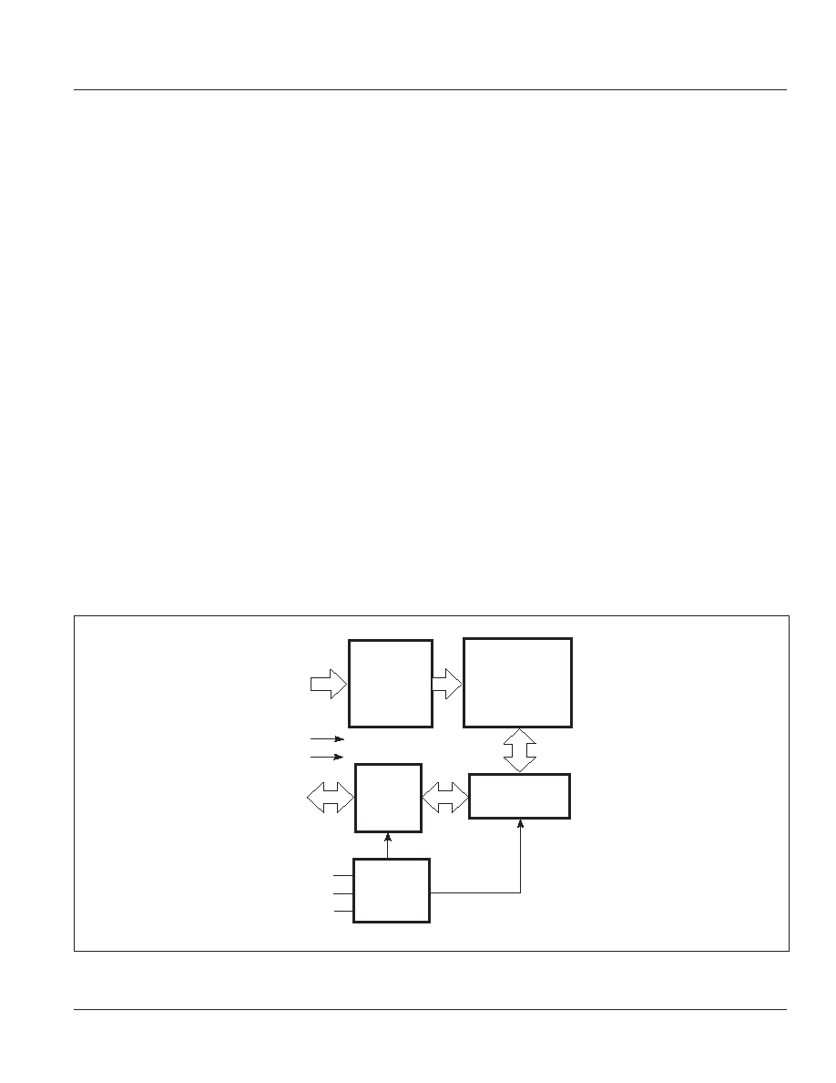
FUNCTIONAL BLOCK DIAGRAM
A0-A19
CE
OE
WE
1M X 8
MEMORY ARRAY
DECODER
COLUMN I/O
CONTROL
CIRCUIT
GND
VDD
I/O
DATA
CIRCUIT
I/O0-I/O7
2
Integrated Silicon Solution, Inc. -- www.issi.com --
1-800-379-4774
Rev. C
04/13/06
IS61LV10248
ISSI
Æ
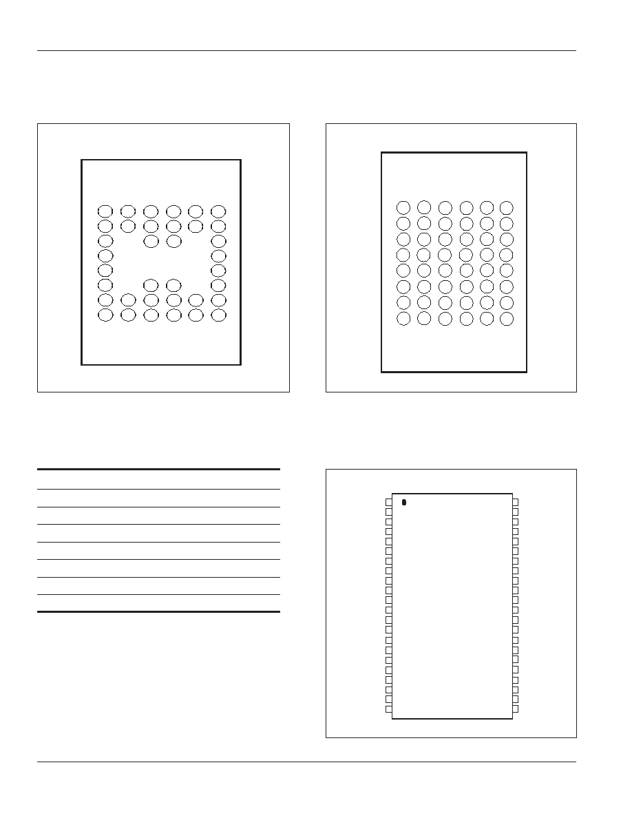
PIN CONFIGURATION
36 mini BGA (B) (9mm x 11mm)
PIN DESCRIPTIONS
A0-A19
Address Inputs
CE
Chip Enable Input
OE
Output Enable Input
WE
Write Enable Input
I/O0-I/O7
Data Input / Output
V
DD
Power
GND
Ground
NC
No Connection
48-pin Mini BGA (M ) (9mm x 11mm)
44-pin TSOP (Type II )
1 2 3 4 5 6
A
B
C
D
E
F
G
H
A0
I/O4
I/O5
GND
V
DD
I/O6
I/O7
A9
A1
A2
OE
A10
NC
WE
A19
A18
CE
A11
A3
A4
A5
A17
A16
A12
A6
A7
A15
A13
A8
I/O0
I/O1
V
DD
GND
I/O2
I/O3
A14
1 2 3 4 5 6
A
B
C
D
E
F
G
H
NC
NC
NC
GND
V
DD
NC
NC
A18
OE
NC
NC
NC
NC
NC
NC
A8
A0
A3
A5
A17
NC
A14
A12
A9
A1
A4
A6
A7
A16
A15
A13
A10
A2
CE
I/O1
I/O3
I/O4
I/O5
WE
A11
NC
I/O0
I/O2
V
DD
GND
I/O6
I/O7
A19
1
2
3
4
5
6
7
8
9
10
11
12
13
14
15
16
17
18
19
20
21
22
40
39
38
37
36
35
34
33
32
31
30
29
28
27
26
25
24
23
NC
NC
A0
A1
A2
A3
A4
CE
I/O0
I/O1
VDD
GND
I/O2
I/O3
WE
A5
A6
A7
A8
A9
NC
NC
NC
NC
NC
A18
A17
A16
A15
OE
I/O7
I/O6
GND
VDD
I/O5
I/O4
A14
A13
A12
A11
A10
A19
NC
NC
44
43
42
41

Integrated Silicon Solution, Inc. -- www.issi.com --
1-800-379-4774
3
Rev. C
04/13/06
IS61LV10248
ISSI
Æ
ABSOLUTE MAXIMUM RATINGS
(1)
Symbol
Parameter
Value
Unit
V
TERM
Terminal Voltage with Respect to GND
≠0.5 to V
DD
+ 0.5
V
V
DD
V
DD
Relates to GND
≠0.3 to 4.0
V
T
STG
Storage Temperature
≠65 to +150
∞C
P
T
Power Dissipation
1.0
W
Notes:
1. Stress greater than those listed under ABSOLUTE MAXIMUM RATINGS may cause permanent damage
to the device. This is a stress rating only and functional operation of the device at these or any other
conditions above those indicated in the operational sections of this specification is not implied. Exposure
to absolute maximum rating conditions for extended periods may affect reliability.
TRUTH TABLE
Mode
WE
WE
WE
WE
WE
CE
CE
CE
CE
CE
OE
OE
OE
OE
OE
I/O Operation
V
DD
Current
Not Selected
X
H
X
High-Z
I
SB
1
, I
SB
2
(Power-down)
Output Disabled H
L
H
High-Z
I
CC
Read
H
L
L
D
OUT
I
CC
Write
L
L
X
D
IN
I
CC
OPERATING RANGE
Range
Ambient Temperature
V
DD
Commercial
0∞C to +70∞C
3.3V +10%, -5%
Industrial
≠40∞C to +85∞C
3.3V +10%, -5%
CAPACITANCE
(1,2)
Symbol
Parameter
Conditions
Max.
Unit
C
IN
Input Capacitance
V
IN
= 0V
6
pF
C
I/O
Input/Output Capacitance
V
OUT
= 0V
8
pF
Notes:
1. Tested initially and after any design or process changes that may affect these parameters.
2. Test conditions: T
A
= 25∞C, f = 1 MHz, V
DD
= 3.3V.

4
Integrated Silicon Solution, Inc. -- www.issi.com --
1-800-379-4774
Rev. C
04/13/06
IS61LV10248
ISSI
Æ
DC ELECTRICAL CHARACTERISTICS
(Over Operating Range)
Symbol Parameter
Test Conditions
Min.
Max.
Unit
V
OH
Output HIGH Voltage
V
DD
= Min., I
OH
= ≠4.0 mA
2.4
--
V
V
OL
Output LOW Voltage
V
DD
= Min., I
OL
= 8.0 mA
--
0.4
V
V
IH
Input HIGH Voltage
2.2
V
DD
+ 0.3
V
V
IL
Input LOW Voltage
(1)
≠0.3
0.8
V
I
LI
Input Leakage
GND
V
IN
V
DD
Com.
≠1
1
µA
Ind.
≠5
5
I
LO
Output Leakage
GND
V
OUT
V
DD
, Outputs Disabled
Com.
≠1
1
µA
Ind.
≠5
5
Note:
1. V
IL
= ≠3.0V for pulse width less than 10 ns.
POWER SUPPLY CHARACTERISTICS
(1)
(Over Operating Range)
-8
-10
Symbol Parameter
Test Conditions
Min.
Max.
Min.
Max.
Unit
I
CC
V
DD
Dynamic Operating
V
DD
= Max.,
Com.
--
110
--
100
mA
Supply Current
I
OUT
= 0 mA, f = f
MAX
Ind.
--
120
--
110
I
SB
1
TTL Standby Current
V
DD
= Max.,
Com.
--
30
--
30
mA
(TTL Inputs)
V
IN
= V
IH
or V
IL
Ind.
--
35
--
35
CE
V
IH
, f = 0
I
SB
2
CMOS Standby
V
DD
= Max.,
Com.
--
20
--
20
mA
Current (CMOS Inputs)
CE
V
DD
≠ 0.2V,
Ind.
--
25
--
25
V
IN
V
DD
≠ 0.2V, or
V
IN
0.2V, f = 0
Note:
1. At f = f
MAX
, address and data inputs are cycling at the maximum frequency, f = 0 means no input lines change.
Integrated Silicon Solution, Inc. -- www.issi.com --
1-800-379-4774
5
Rev. C
04/13/06
IS61LV10248
ISSI
Æ
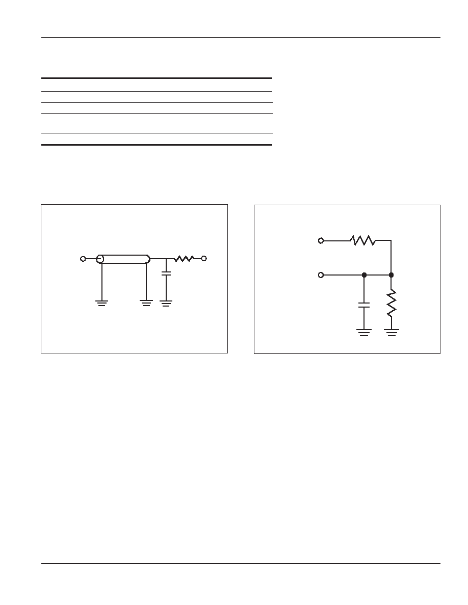
AC TEST LOADS
AC TEST CONDITIONS
Parameter
Unit
Input Pulse Level
0V to 3.0V
Input Rise and Fall Times
3 ns
Input and Output Timing
1.5V
and Reference Levels
Output Load
See Figures 1 and 2
Figure 1
319
5 pF
Including
jig and
scope
353
OUTPUT
3.3V
Figure 2
Z
O
= 50
1.5V
50
OUTPUT
30 pF
Including
jig and
scope
6
Integrated Silicon Solution, Inc. -- www.issi.com --
1-800-379-4774
Rev. C
04/13/06
IS61LV10248
ISSI
Æ
READ CYCLE SWITCHING CHARACTERISTICS
(1)
(Over Operating Range)
-8
-10
Symbol
Parameter
Min.
Max.
Min.
Max.
Unit
t
RC
Read Cycle Time
8
--
10
--
ns
t
AA
Address Access Time
--
8
--
10
ns
t
OHA
Output Hold Time
3
--
3
--
ns
t
ACE
CE Access Time
--
8
--
10
ns
t
DOE
OE Access Time
--
3.5
--
4
ns
t
HZOE
(2)
OE to High-Z Output
--
3
--
4
ns
t
LZOE
(2)
OE to Low-Z Output
0
--
0
--
ns
t
HZCE
(2
CE to High-Z Output
--
3
0
4
ns
t
LZCE
(2)
CE to Low-Z Output
3
--
3
--
ns
t
PU
Power Up Time
0
--
0
--
ns
t
PD
Power Down Time
--
8
--
10
ns
Notes:
1. Test conditions assume signal transition times of 3 ns or less, timing reference levels of 1.5V, input pulse
levels of 0V to 3.0V and output loading specified in Figure 1.
2. Tested with the load in Figure 2. Transition is measured ±500 mV from steady-state voltage.
Integrated Silicon Solution, Inc. -- www.issi.com --
1-800-379-4774
7
Rev. C
04/13/06
IS61LV10248
ISSI
Æ
t
RC
t
OHA
t
AA
t
DOE
t
LZOE
t
ACE
t
LZCE
t
HZOE
HIGH-Z
DATA VALID
CE_RD2.eps
ADDRESS
OE
CE
D
OUT
t
HZCE
READ CYCLE NO. 2
(1,3)
(
CE and OE Controlled)
Notes:
1.
WE is HIGH for a Read Cycle.
2. The device is continuously selected.
OE, CE = V
IL
.
3. Address is valid prior to or coincident with
CE LOW transitions.
AC WAVEFORMS
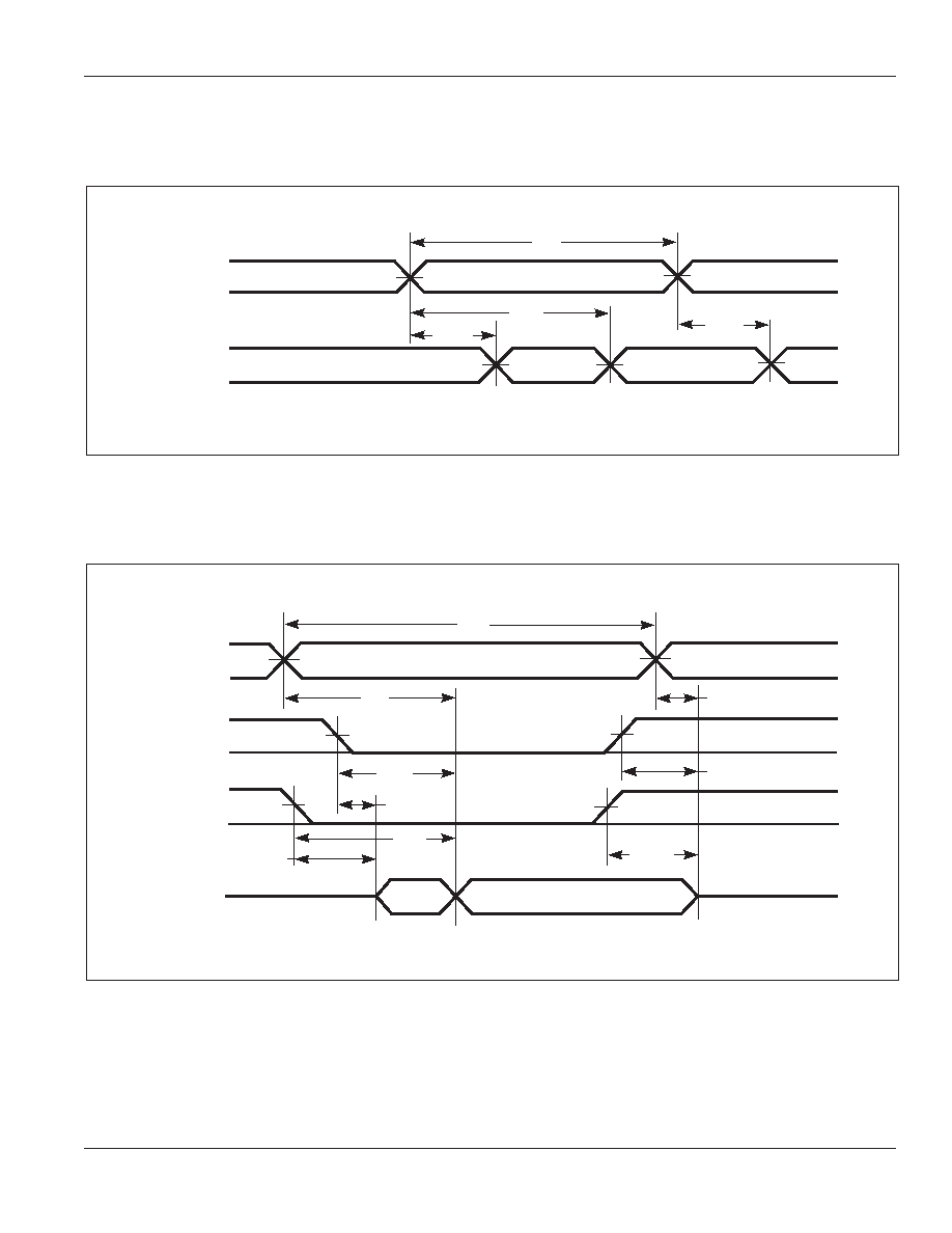
READ CYCLE NO. 1
(1,2)
(Address Controlled) (
CE = OE = V
IL
)
DATA VALID
READ1.eps
PREVIOUS DATA VALID
t
AA
t
OHA
t
OHA
t
RC
D
OUT
ADDRESS

8
Integrated Silicon Solution, Inc. -- www.issi.com --
1-800-379-4774
Rev. C
04/13/06
IS61LV10248
ISSI
Æ
WRITE CYCLE SWITCHING CHARACTERISTICS
(1,3)
(Over Operating Range)
-8
-10
Symbol
Parameter
Min.
Max.
Min.
Max.
Unit
t
WC
Write Cycle Time
8
--
10
--
ns
t
SCE
CE to Write End
6.5
--
8
--
ns
t
AW
Address Setup Time
6.5
--
8
--
ns
to Write End
t
HA
Address Hold from Write End
0
--
0
--
ns
t
SA
Address Setup Time
0
--
0
--
ns
t
PWE
1
WE Pulse Width
6.5
--
8
--
ns
t
PWE
2
WE Pulse Width (OE = LOW)
8
--
10
--
ns
t
SD
Data Setup to Write End
5
--
6
--
ns
t
HD
Data Hold from Write End
0
--
0
--
ns
t
HZWE
(2)
WE LOW to High-Z Output
--
3.5
--
5
ns
t
LZWE
(2)
WE HIGH to Low-Z Output
2
--
2
--
ns
Notes:
1. Test conditions assume signal transition times of 3 ns or less, timing reference levels of 1.5V, input pulse levels of 0V to 3.0V
and output loading specified in Figure 1.
2. Tested with the load in Figure 2. Transition is measured ±500 mV from steady-state voltage. Not 100% tested.
3. The internal write time is defined by the overlap of
CE LOW and WE LOW. All signals must be in valid states to initiate a Write,
but any one can go inactive to terminate the Write. The Data Input Setup and Hold timing are referenced to the rising or falling
edge of the signal that terminates the write.
Integrated Silicon Solution, Inc. -- www.issi.com --
1-800-379-4774
9
Rev. C
04/13/06
IS61LV10248
ISSI
Æ
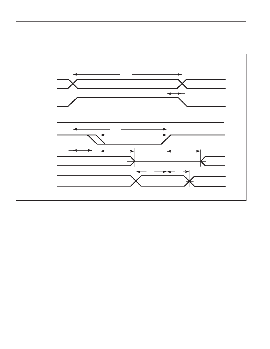
AC WAVEFORMS
WRITE CYCLE NO. 1
(1,2)
(
CE Controlled, OE = HIGH or LOW)
DATA UNDEFINED
t
WC
VALID ADDRESS
t
SCE
t
PWE1
t
PWE2
t
AW
t
HA
HIGH-Z
t
HD
t
SA
t
HZWE
ADDRESS
CE
WE
D
OUT
D
IN
DATA
IN
VALID
t
LZWE
t
SD
CE_WR1.eps
10
Integrated Silicon Solution, Inc. -- www.issi.com --
1-800-379-4774
Rev. C
04/13/06
IS61LV10248
ISSI
Æ
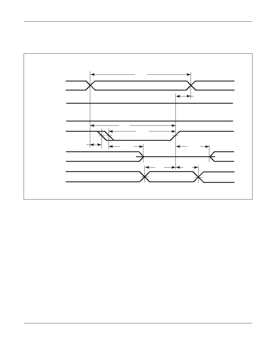
DATA UNDEFINED
LOW
t
WC
VALID ADDRESS
t
PWE1
t
AW
t
HA
HIGH-Z
t
HD
t
SA
t
HZWE
ADDRESS
CE
WE
D
OUT
D
IN
OE
DATA
IN
VALID
t
LZWE
t
SD
CE_WR2.eps
Notes:
1. The internal write time is defined by the overlap of
CE LOW and WE LOW. All signals must be in valid states to initiate a Write, but
any one can go inactive to terminate the Write. The Data Input Setup and Hold timing are referenced to the rising or falling edge of
the signal that terminates the Write.
2. I/O will assume the High-Z state if
OE > V
IH
.
AC WAVEFORMS
WRITE CYCLE NO. 2
(1,2)
(
WE Controlled: OE is HIGH During Write Cycle)
Integrated Silicon Solution, Inc. -- www.issi.com --
1-800-379-4774
11
Rev. C
04/13/06
IS61LV10248
ISSI
Æ
AC WAVEFORMS
WRITE CYCLE NO. 3
(
WE Controlled: OE is LOW During Write Cycle)
DATA UNDEFINED
t
WC
VALID ADDRESS
LOW
LOW
t
PWE2
t
AW
t
HA
HIGH-Z
t
HD
t
SA
t
HZWE
ADDRESS
CE
WE
D
OUT
D
IN
OE
DATA
IN
VALID
t
LZWE
t
SD
CE_WR3.eps

12
Integrated Silicon Solution, Inc. -- www.issi.com --
1-800-379-4774
Rev. C
04/13/06
IS61LV10248
ISSI
Æ
ORDERING INFORMATION
Commercial Range: 0∞C to +70∞C
Speed (ns)
Order Part No.
Package
8
IS61LV10248-8M
48 mini BGA (9mm x 11mm)
IS61LV10248-8T
TSOP (Type II)
IS61LV10248-8B
36 mini BGA (9mm x 11mm)
10
IS61LV10248-10T
TSOP (Type II)
Industrial Range: -40∞C to +85∞C
Speed (ns)
Order Part No.
Package
8
IS61LV10248-8MI
48 mini BGA (9mm x 11mm)
IS61LV10248-8TI
TSOP (Type II)
IS61LV10248-8BI
36 mini BGA (9mm x 11mm)
10
IS61LV10248-10MI
48 mini BGA (9mm x 11mm)
IS61LV10248-10TI
TSOP (Type II)
IS61LV10248-10TLI
TSOP (Type II), Lead-free
IS61LV10248-10BI
36 mini BGA (9mm x 11m)
IS61LV10248-10BLI
36 mini BGA (9mm x 11m), Lead-free
Integrated Silicon Solution, Inc. -- www.issi.com --
1-800-379-4774
13
Rev. C
04/13/06
IS61LV10248
ISSI
Æ
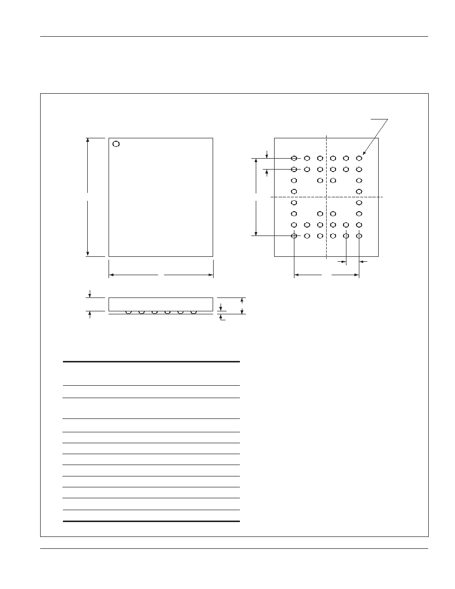
Mini Ball Grid Array
Package Code: B (36-pin)
Notes:
1. Controlling dimensions are in millimeters.
mBGA - 9mm x 11mm
MILLIMETERS
INCHES
Sym.
Min. Typ. Max.
Min. Typ. Max.
N0.
Leads
36
A
--
--
1.20
--
--
0.047
A1
0.24
--
0.30
0.009
--
0.012
A2
0.60
--
--
0.024
--
--
D
10.90 11.00 11.10
0.429 0.433 0.437
D1
5.25 BSC
0.207 BSC
E
8.90
9.00
9.10
0.350 0.354 0.358
E1
3.75 BSC
0.148 BSC
e
0.75 BSC
0.030 BSC
b
0.30
0.35
0.40
0.012 0.014 0.016
SEATING PLANE
A
A1
A2
A
B
C
D
E
F
G
H
e
e
D1
E1
E
D
b (36x)
Top View
Bottom View
6 5 4 3 2 1
1 2 3 4 5 6
A
B
C
D
E
F
G
H
PACKAGING INFORMATION
ISSI
Æ
Integrated Silicon Solution, Inc. -- www.issi.com --
1-800-379-4774
Rev. D
01/15/03
Copyright © 2003 Integrated Silicon Solution, Inc. All rights reserved. ISSI reserves the right to make changes to this specification and its products at any time
without notice. ISSI assumes no liability arising out of the application or use of any information, products or services described herein. Customers are advised to
obtain the latest version of this device specification before relying on any published information and before placing orders for products.
Mini Ball Grid Array
Package Code: M (48-pin)
Notes:
1. Controlling dimensions are in millimeters.
SEATING PLANE
A
A1
A2
A
B
C
D
E
F
G
H
e
e
D1
E1
E
D
b (48x)
Top View
Bottom View
6 5 4 3 2 1
1 2 3 4 5 6
A
B
C
D
E
F
G
H
PACKAGING INFORMATION
ISSI
Æ
2
Integrated Silicon Solution, Inc. -- www.issi.com --
1-800-379-4774
Rev. D
01/15/03
mBGA - 7.2mm x 8.7mm
MILLIMETERS
INCHES
Sym.
Min. Typ. Max.
Min. Typ. Max.
N0.
Leads
48
A
--
--
1.20
--
--
0.047
A1
0 .24
--
0.30
0.009
--
0.012
A2
0.60
--
--
0.024
--
--
D
8.60
8.70
8.80
0.339 0.343 0.346
D1
5.25BSC
0.207BSC
E
7.10
7.20
7.30
0.280 0.283 0.287
E1
3.75BSC
0.148BSC
e
0.75BSC
0.030BSC
b
0.30
0.35
0.40
0.012 0.014 0.016
mBGA - 9mm x 11mm
MILLIMETERS
INCHES
Sym.
Min. Typ. Max.
Min. Typ. Max.
N0.
Leads
48
A
--
--
1.20
--
--
0.047
A1
0.24
--
0.30
0.009
--
0.012
A2
0.60
--
--
0.024
--
--
D
10.90 11.00 11.10
0.429 0.433 0.437
D1
5.25BSC
0.207BSC
E
8.90
9.00
9.10
0.350 0.354 0.358
E1
3.75BSC
0.148BSC
e
0.75BSC
0.030BSC
b
0.30
0.35
0.40
0.012 0.014 0.016
mBGA - 6mm x 8mm
MILLIMETERS
INCHES
Sym.
Min. Typ. Max.
Min. Typ. Max.
N0.
Leads
48
A
--
--
1.20
.--
--
0.047
A1
0.25
--
0.40
0.010
-- 0.016
A2
0.60
--
--
0.024
--
--
D
7.90
8.00
8.10
0.311 0.314 0.319
D1
5.60BSC
0.220BSC
E
5.90
6.00
6.10
0.232 0.236 0.240
E1
4.00BSC
0.157BSC
e
0.80BSC
0.031BSC
b
0.40
0.45
0.50
0.016 0.018 0.020
Mini Ball Grid Array
Package Code: M (48-pin)
PACKAGING INFORMATION
ISSI
Æ
Integrated Silicon Solution, Inc. -- www.issi.com --
1-800-379-4774
Rev. F
06/18/03
Copyright © 2003 Integrated Silicon Solution, Inc. All rights reserved. ISSI reserves the right to make changes to this specification and its products at any time
without notice. ISSI assumes no liability arising out of the application or use of any information, products or services described herein. Customers are advised to
obtain the latest version of this device specification before relying on any published information and before placing orders for products.
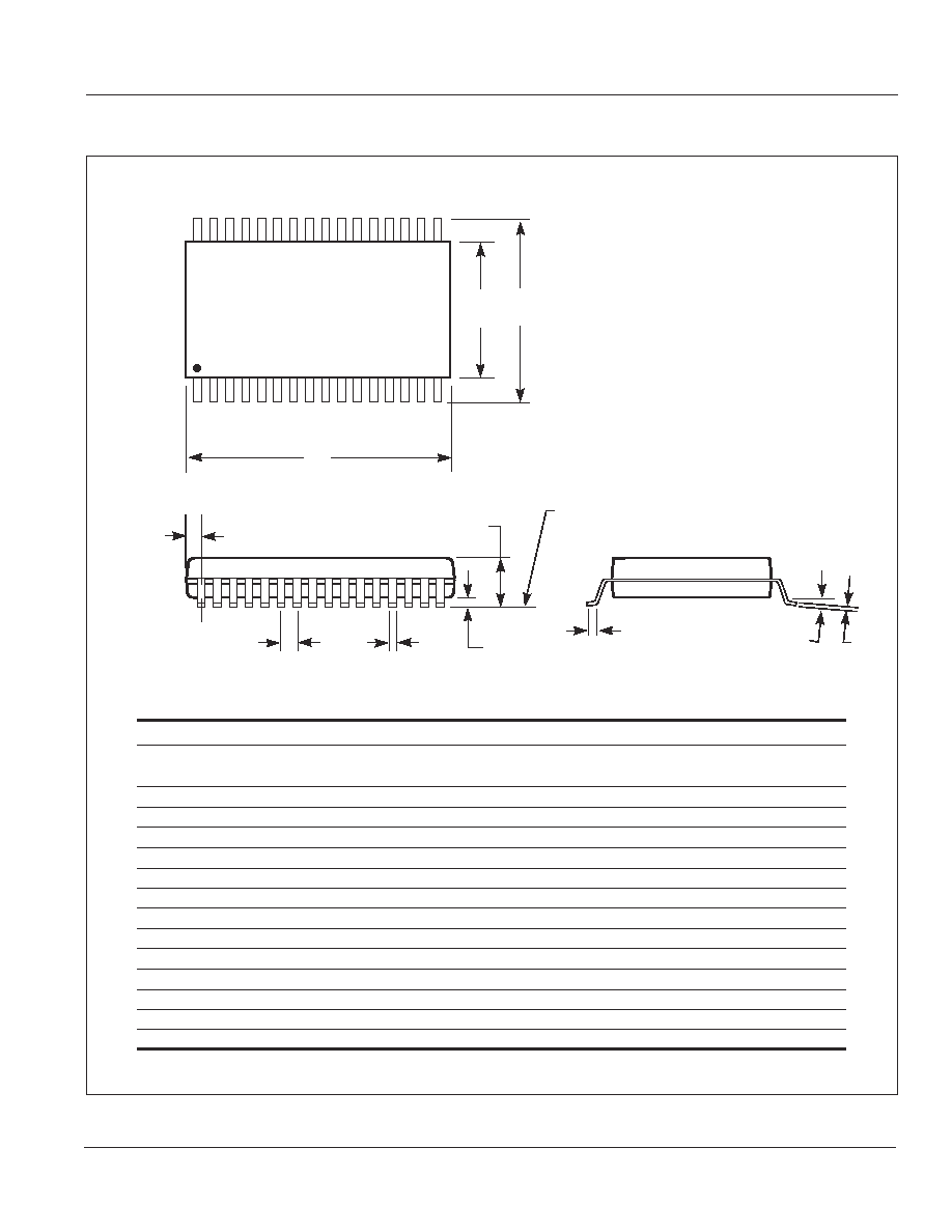
Plastic TSOP
Package Code: T (Type II)
D
SEATING PLANE
b
e
C
1
N/2
N/2+1
N
E1
A1
A
E
L
ZD
.
Notes:
1. Controlling dimension: millimieters,
unless otherwise specified.
2. BSC = Basic lead spacing
between centers.
3. Dimensions D and E1 do not
include mold flash protrusions and
should be measured from the
bottom of the package.
4. Formed leads shall be planar with
respect to one another within
0.004 inches at the seating plane.
Plastic TSOP (T - Type II)
Millimeters
Inches
Millimeters
Inches
Millimeters
Inches
Symbol Min
Max
Min
Max
Min
Max
Min
Max
Min
Max
Min
Max
Ref. Std.
No. Leads (N)
32
44
50
A
--
1.20
--
0.047
--
1.20
--
0.047
--
1.20
--
0.047
A1
0.05
0.15
0.002 0.006
0.05
0.15
0.002 0.006
0.05
0.15
0.002 0.006
b
0.30
0.52
0.012 0.020
0.30
0.45
0.012 0.018
0.30
0.45
0.012 0.018
C
0.12
0.21
0.005 0.008
0.12
0.21
0.005 0.008
0.12
0.21
0.005 0.008
D
20.82 21.08
0.820 0.830
18.31 18.52
0.721 0.729
20.82 21.08
0.820 0.830
E1
10.03 10.29
0.391 0.400
10.03 10.29
0.395 0.405
10.03 10.29
0.395 0.405
E
11.56 11.96
0.451 0.466
11.56 11.96
0.455 0.471
11.56 11.96
0.455 0.471
e
1.27 BSC
0.050 BSC
0.80 BSC
0.032 BSC
0.80 BSC
0.031 BSC
L
0.40
0.60
0.016 0.024
0.41
0.60
0.016 0.024
0.40
0.60
0.016 0.024
ZD 0.95 REF 0.037 REF 0.81 REF 0.032 REF 0.88 REF 0.035 REF
0∞
5∞
0∞
5∞
0∞
5∞
0∞
5∞
0∞
5∞
0∞
5∞