
Integrated Silicon Solution, Inc. -- 1-800-379-4774
1
Rev. A
11/30/00
IS61LV12816
ISSI
Æ
FEATURES
∑ High-speed access time: 8, 10, 12, and 15 ns
∑ CMOS low power operation
∑ TTL and CMOS compatible interface levels
∑ Single 3.3V ± 10% power supply
∑ Fully static operation: no clock or refresh
required
∑ Three state outputs
∑ Data control for upper and lower bytes
∑ Industrial temperature available
128K x 16 HIGH-SPEED CMOS STATIC RAM
WITH 3.3V SUPPLY
DESCRIPTION
The
ISSI
IS61LV12816 is a high-speed, 2,097,152-bit static
RAM organized as 131,072 words by 16 bits. It is fabricated
using
ISSI
's high-performance CMOS technology. This highly
reliable process coupled with innovative circuit design
techniques, yields access times as fast as 8 ns with low power
consumption.
When
CE is HIGH (deselected), the device assumes a
standby mode at which the power dissipation can be reduced
down with CMOS input levels.
Easy memory expansion is provided by using Chip Enable and
Output Enable inputs,
CE and OE. The active LOW Write
Enable (
WE) controls both writing and reading of the memory.
A data byte allows Upper Byte (
UB) and Lower Byte (LB)
access.
The IS61LV12816 is packaged in the JEDEC standard 44-pin
400-mil SOJ, 44-pin TSOP, 44-pin LQFP, and 48-pin mini
BGA (6mm x 8mm).
FUNCTIONAL BLOCK DIAGRAM
NOVEMBER 2000
ISSI reserves the right to make changes to its products at any time without notice in order to improve design and supply the best possible product. We assume no responsibility for any errors
which may appear in this publication. © Copyright 2000, Integrated Silicon Solution, Inc.
A0-A16
CE
OE
WE
128K x 16
MEMORY ARRAY
DECODER
COLUMN I/O
CONTROL
CIRCUIT
GND
VCC
I/O
DATA
CIRCUIT
I/O0-I/O7
Lower Byte
I/O8-I/O15
Upper Byte
UB
LB
Integrated Silicon Solution, Inc. -- 1-800-379-4774
1
Rev. A
11/30/00
IS61LV12816
2
Integrated Silicon Solution, Inc. -- 1-800-379-4774
Rev. A
11/30/00
ISSI
Æ
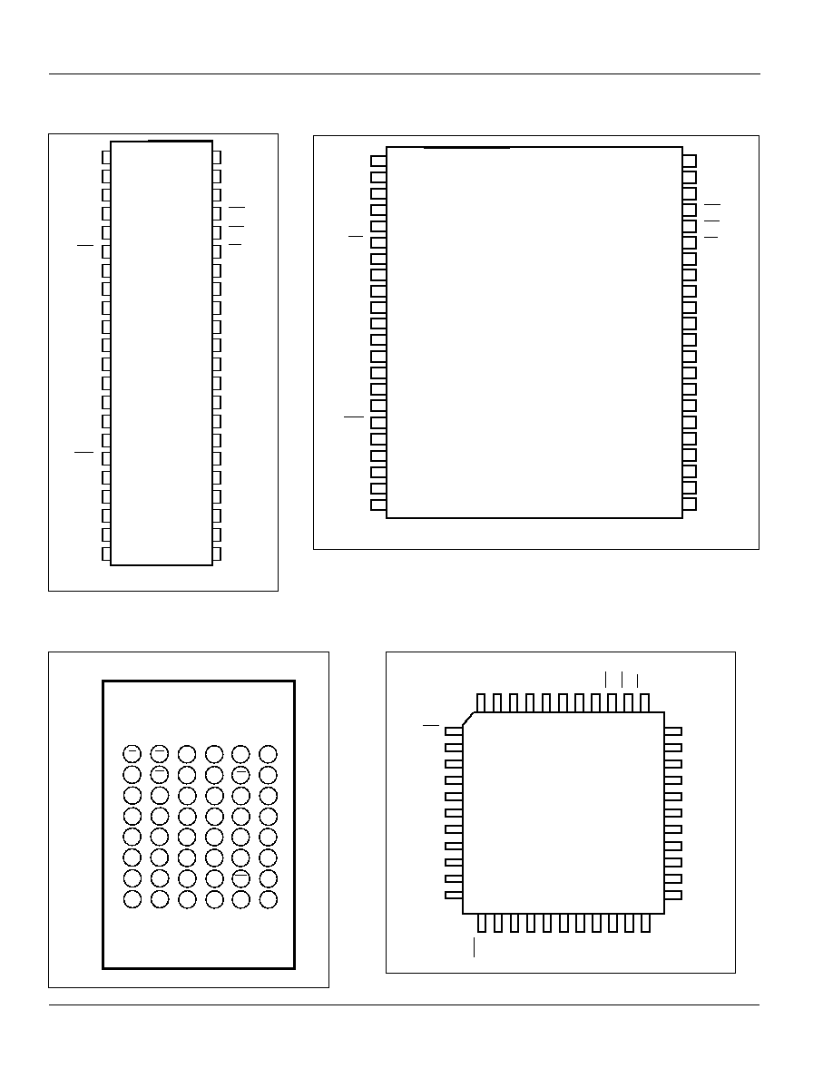
PIN CONFIGURATIONS
44-Pin SOJ (K)
1
2
3
4
5
6
7
8
9
10
11
12
13
14
15
16
17
18
19
20
21
22
44
43
42
41
40
39
38
37
36
35
34
33
32
31
30
29
28
27
26
25
24
23
A4
A3
A2
A1
A0
CE
I/O0
I/O1
I/O2
I/O3
Vcc
GND
I/O4
I/O5
I/O6
I/O7
WE
A16
A15
A14
A13
A12
A5
A6
A7
OE
UB
LB
I/O15
I/O14
I/O13
I/O12
GND
Vcc
I/O11
I/O10
I/O9
I/O8
NC
A8
A9
A10
A11
NC
44-Pin TSOP (T)
48-Pin mini BGA (B)
1 2 3 4 5 6
A
B
C
D
E
F
G
H
LB
OE
A0
A1
A2
N/C
I/O
8
UB
A3
A4
CE
I/O
0
I/O
9
I/O
10
A5
A6
I/O
1
I/O
2
GND
I/O
11
NC
A7
I/O
3
Vcc
Vcc
I/O
12
NC
A16
I/O
4
GND
I/O
14
I/O
13
A14
A15
I/O
5
I/O
6
I/O
15
NC
A12
A13
WE
I/O
7
NC
A8
A9
A10
A11
NC
44-Pin LQFP (LQ)
1
2
3
4
5
6
7
8
9
10
11
33
32
31
30
29
28
27
26
25
24
23
12 13 14 15 16 17 18 19 20 21 22
44 43 42 41 40 39 38 37 36 35 345
CE
I/O0
I/O1
I/O2
I/O3
Vcc
GND
I/O4
I/O5
I/O6
I/O7
I/O15
I/O14
I/O13
I/O12
GND
Vcc
I/O11
I/O10
I/O9
I/O8
NC
TOP VIEW
WE
A0
A1
A2
A3
A4
NC
A5
A6
A7
A8
A16
A15
A14
A13
A12
A11
A10
A9
OE
UB
LB
IS61LV12816
Integrated Silicon Solution, Inc. -- 1-800-379-4774
3
Rev. A
11/30/00
ISSI
Æ
OPERATING RANGE
Range
Ambient Temperature
V
CC
Commercial
0∞C to + 70∞C
3.3V ± 10%
Industrial
≠40∞C to + 85∞C
3.3V ± 10%
DC ELECTRICAL CHARACTERISTICS
(Over Operating Range)
Symbol
Parameter
Test Conditions
Min.
Max.
Unit
V
OH
Output HIGH Voltage
V
CC
= Min., I
OH
= ≠4.0 mA
2.4
--
V
V
OL
Output LOW Voltage
V
CC
= Min., I
OL
= 8.0 mA
--
0.4
V
V
IH
Input HIGH Voltage
(1)
2
V
CC
+ 0.3
V
V
IL
Input LOW Voltage
(1)
≠0.3
0.8
V
I
LI
Input Leakage
GND - V
IN
- V
CC
≠1
1
µA
I
LO
Output Leakage
GND - V
OUT
- V
CC
, Outputs Disabled
≠1
1
µA
Note:
1. V
IL
(min.) = ≠0.3V DC; V
IL
(min.) = ≠2.0V AC (pulse width - 2.0 ns).
V
IH
(max.) = V
CC
+ 0.3V DC; V
IH
(max.) = V
CC
+ 2.0V AC (pulse width - 2.0 ns).
PIN DESCRIPTIONS
A0-A16
Address Inputs
I/O0-I/O15
Data Inputs/Outputs
CE
Chip Enable Input
OE
Output Enable Input
WE
Write Enable Input
LB
Lower-byte Control (I/O0-I/O7)
UB
Upper-byte Control (I/O8-I/O15)
NC
No Connection
Vcc
Power
GND
Ground
ABSOLUTE MAXIMUM RATINGS
(1)
Symbol
Parameter
Value
Unit
V
CC
Power Supply Voltage Relative to GND
≠0.5 to 5.0
V
V
TERM
Terminal Voltage with Respect to GND
≠0.5 to Vcc + 0.5
V
T
STG
Storage Temperature
≠65 to + 150
∞C
T
BIAS
Temperature Under Bias:
Com.
≠10 to + 85
∞C
Ind.
≠45 to + 90
∞C
P
T
Power Dissipation
2.0
W
I
OUT
DC Output Current
±20
mA
Note:
1. Stress greater than those listed under ABSOLUTE MAXIMUM RATINGS may cause permanent
damage to the device. This is a stress rating only and functional operation of the device at these or
any other conditions above those indicated in the operational sections of this specification is not
implied. Exposure to absolute maximum rating conditions for extended periods may affect reliability.
IS61LV12816
4
Integrated Silicon Solution, Inc. -- 1-800-379-4774
Rev. A
11/30/00
ISSI
Æ
POWER SUPPLY CHARACTERISTICS
(1)
(Over Operating Range)
-8 ns
-10 ns
-12 ns
-15 ns
Symbol
Parameter
Test Conditions
Min. Max.
Min. Max.
Min. Max.
Min. Max.
Unit
I
CC
Vcc Operating
V
CC
= Max.,
CE = V
IL
Com.
--
150
--
125
--
110
--
90
mA
Supply Current
I
OUT
= 0 mA, f = Max.
Ind.
--
160
--
135
--
120
--
100
I
SB
1
TTL Standby
V
CC
= Max.,
Com.
--
50
--
40
--
35
--
30
mA
Current
V
IN
= V
IH
or V
IL
Ind.
--
60
--
50
--
45
--
40
(TTL Inputs)
CE ∑ V
IH
, f = max
I
SB
2
CMOS Standby
V
CC
= Max.,
Com.
--
10
--
10
--
10
--
10
mA
Current
CE - V
CC
≠ 0.2V,
Ind.
--
20
--
20
--
20
--
20
(CMOS Inputs)
V
IN
> V
CC
≠ 0.2V, or
V
IN
- 0.2V, f = 0
Note:
1. At f = f
MAX
, address and data inputs are cycling at the maximum frequency, f = 0 means no input lines change.
TRUTH TABLE
I/O PIN
Mode
WE
CE
OE
LB
UB
I/O0-I/O7
I/O8-I/O15
Vcc Current
Not Selected
X
H
X
X
X
High-Z
High-Z
I
SB
1
, I
SB
2
Output Disabled
H
L
H
X
X
High-Z
High-Z
I
CC
X
L
X
H
H
High-Z
High-Z
Read
H
L
L
L
H
D
OUT
High-Z
I
CC
H
L
L
H
L
High-Z
D
OUT
H
L
L
L
L
D
OUT
D
OUT
Write
L
L
X
L
H
D
IN
High-Z
I
CC
L
L
X
H
L
High-Z
D
IN
L
L
X
L
L
D
IN
D
IN
IS61LV12816
Integrated Silicon Solution, Inc. -- 1-800-379-4774
5
Rev. A
11/30/00
ISSI
Æ
READ CYCLE SWITCHING CHARACTERISTICS
(1)
(Over Operating Range)
-8 ns
-10 ns
-12 ns
-15 ns
Symbol
Parameter
Min.
Max
Min.
Max.
Min.
Max.
Min.
Max.
Unit
t
RC
Read Cycle Time
8
--
10
--
12
--
15
--
ns
t
AA
Address Access Time
--
8
--
10
--
12
--
15
ns
t
OHA
Output Hold Time
3
--
3
--
3
--
3
--
ns
t
ACE
CE Access Time
8
--
--
10
--
12
--
15
ns
t
DOE
OE Access Time
--
3
--
4
--
5
--
6
ns
t
HZOE
(2)
OE to High-Z Output
--
3
--
4
--
5
0
6
ns
t
LZOE
(2)
OE to Low-Z Output
0
--
0
--
0
--
0
--
ns
t
HZCE
(2)
CE to High-Z Output
0
3
0
4
0
5
0
8
ns
t
LZCE
(2)
CE to Low-Z Output
3
--
3
--
3
--
3
--
ns
t
BA
LB, UB Access Time
--
3
--
4
--
5
--
6
ns
t
HZB
(2)
LB, UB to High-Z Output
0
3
0
4
0
5
0
6
ns
t
LZB
(2)
LB, UB to Low-Z Output
0
--
0
--
0
--
0
--
ns
Notes:
1. Test conditions assume signal transition times of 3 ns or less, timing reference levels of 1.5V, input pulse levels
of 0V to 3.0V and output loading specified in Figure 1.
2. Tested with the load in Figure 2. Transition is measured ±500 mV from steady-state voltage. Not 100% tested.
AC TEST CONDITIONS
Parameter
Unit
Input Pulse Level
0V to 3.0V
Input Rise and Fall Times
3 ns
Input and Output Timing
1.5V
and Reference Level
Output Load
See Figures 1 and 2
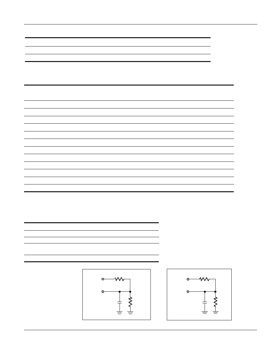
AC TEST LOADS
Figure 1.
319
5 pF
Including
jig and
scope
353
OUTPUT
3.3V
CAPACITANCE
(1)
Symbol
Parameter
Conditions
Max.
Unit
C
IN
Input Capacitance
V
IN
= 0V
6
pF
C
OUT
Input/Output Capacitance
V
OUT
= 0V
8
pF
Note:
1. Tested initially and after any design or process changes that may affect these parameters.
319
30 pF
Including
jig and
scope
353
OUTPUT
3.3V
Figure 2.
IS61LV12816
6
Integrated Silicon Solution, Inc. -- 1-800-379-4774
Rev. A
11/30/00
ISSI
Æ
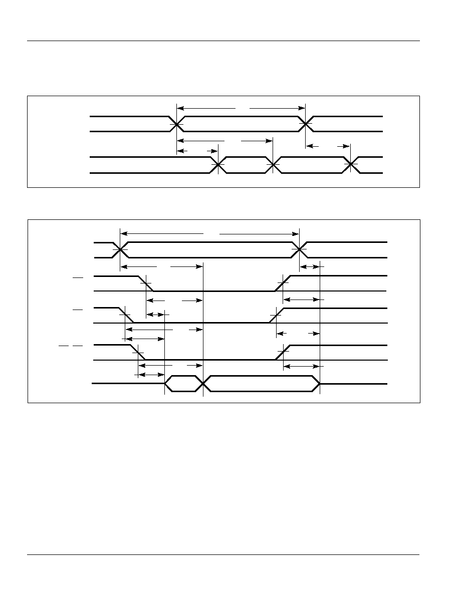
DATA VALID
READ1.eps
PREVIOUS DATA VALID
t
AA
t
OHA
t
OHA
t
RC
D
OUT
ADDRESS
t
RC
t
OHA
t
AA
t
DOE
t
LZOE
t
ACE
t
LZCE
t
HZOE
HIGH-Z
DATA VALID
UB_CEDR2.eps
t
HZB
ADDRESS
OE
CE
LB, UB
D
OUT
t
HZCE
t
BA
t
LZB
READ CYCLE NO. 2
(1,3)
AC WAVEFORMS
READ CYCLE NO. 1
(1,2)
(Address Controlled) (
CE = OE = V
IL
,
UB or LB = V
IL
)
Notes:
1.
WE is HIGH for a Read Cycle.
2. The device is continuously selected.
OE, CE, UB, or LB = V
IL
.
3. Address is valid prior to or coincident with
CE LOW transition.

IS61LV12816
Integrated Silicon Solution, Inc. -- 1-800-379-4774
7
Rev. A
11/30/00
ISSI
Æ
WRITE CYCLE SWITCHING CHARACTERISTICS
(1,3)
(Over Operating Range)
-8 ns
-10 ns
-12 ns
-15 ns
Symbol
Parameter
Min.
Max
Min.
Max.
Min.
Max.
Min.
Max.
Unit
t
WC
Write Cycle Time
8
--
10
--
12
--
15
--
ns
t
SCE
CE to Write End
6.5
--
8
--
8
--
10
--
ns
t
AW
Address Setup Time
6.5
--
8
--
8
--
10
--
ns
to Write End
t
HA
Address Hold from Write End
0
--
0
--
0
--
0
--
ns
t
SA
Address Setup Time
0
--
0
--
0
--
0
--
ns
t
PWB
LB, UB Valid to End of Write
6.5
--
8
--
9
--
10
--
ns
t
PWE
1
WE Pulse Width (OE = HIGH)
5
--
7
--
8
--
10
--
ns
t
PWE
2
WE Pulse Width (OE = LOW)
6.5
--
8
--
10
--
11
--
ns
t
SD
Data Setup to Write End
4
--
5
--
6
--
7
--
ns
t
HD
Data Hold from Write End
0
--
0
--
0
--
0
--
ns
t
HZWE
(3)
WE LOW to High-Z Output
--
3
--
4
--
5
--
6
ns
t
LZWE
(3)
WE HIGH to Low-Z Output
0
--
0
--
0
--
0
--
ns
Notes:
1. Test conditions assume signal transition times of 3 ns or less, timing reference levels of 1.5V, input pulse levels of 0V
to 3.0V and output loading specified in Figure 1.
2. The internal write time is defined by the overlap of
CE LOW and UB or LB, and WE LOW. All signals must be in valid
states to initiate a Write, but any one can go inactive to terminate the Write. The Data Input Setup and Hold timing
are referenced to the rising or falling edge of the signal that terminates the write.
3. Tested with the load in Figure 2. Transition is measured ±500 mV from steady-state voltage. Not 100% tested.
IS61LV12816
8
Integrated Silicon Solution, Inc. -- 1-800-379-4774
Rev. A
11/30/00
ISSI
Æ
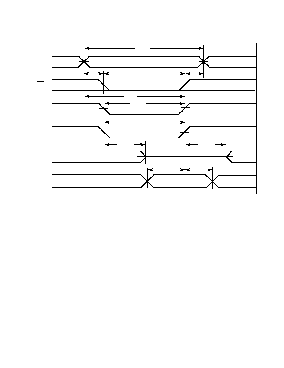
WRITE CYCLE NO. 1
(1,2)
(
CE Controlled, OE = HIGH or LOW)
DATA UNDEFINED
t
WC
VALID ADDRESS
t
SCE
t
PWE1
t
PWE2
t
AW
t
HA
HIGH-Z
t
PBW
t
HD
t
SA
t
HZWE
ADDRESS
CE
UB, LB
WE
D
OUT
D
IN
DATA
IN
VALID
t
LZWE
t
SD
UB_CEWR1.eps
IS61LV12816
Integrated Silicon Solution, Inc. -- 1-800-379-4774
9
Rev. A
11/30/00
ISSI
Æ
WRITE CYCLE NO. 2
(1)
(
WE Controlled, OE = HIGH during Write Cycle)
DATA UNDEFINED
LOW
t
WC
VALID ADDRESS
t
PWE1
t
AW
t
HA
HIGH-Z
t
PBW
t
HD
t
SA
t
HZWE
ADDRESS
CE
UB, LB
WE
D
OUT
D
IN
OE
DATA
IN
VALID
t
LZWE
t
SD
UB_CEWR2.eps
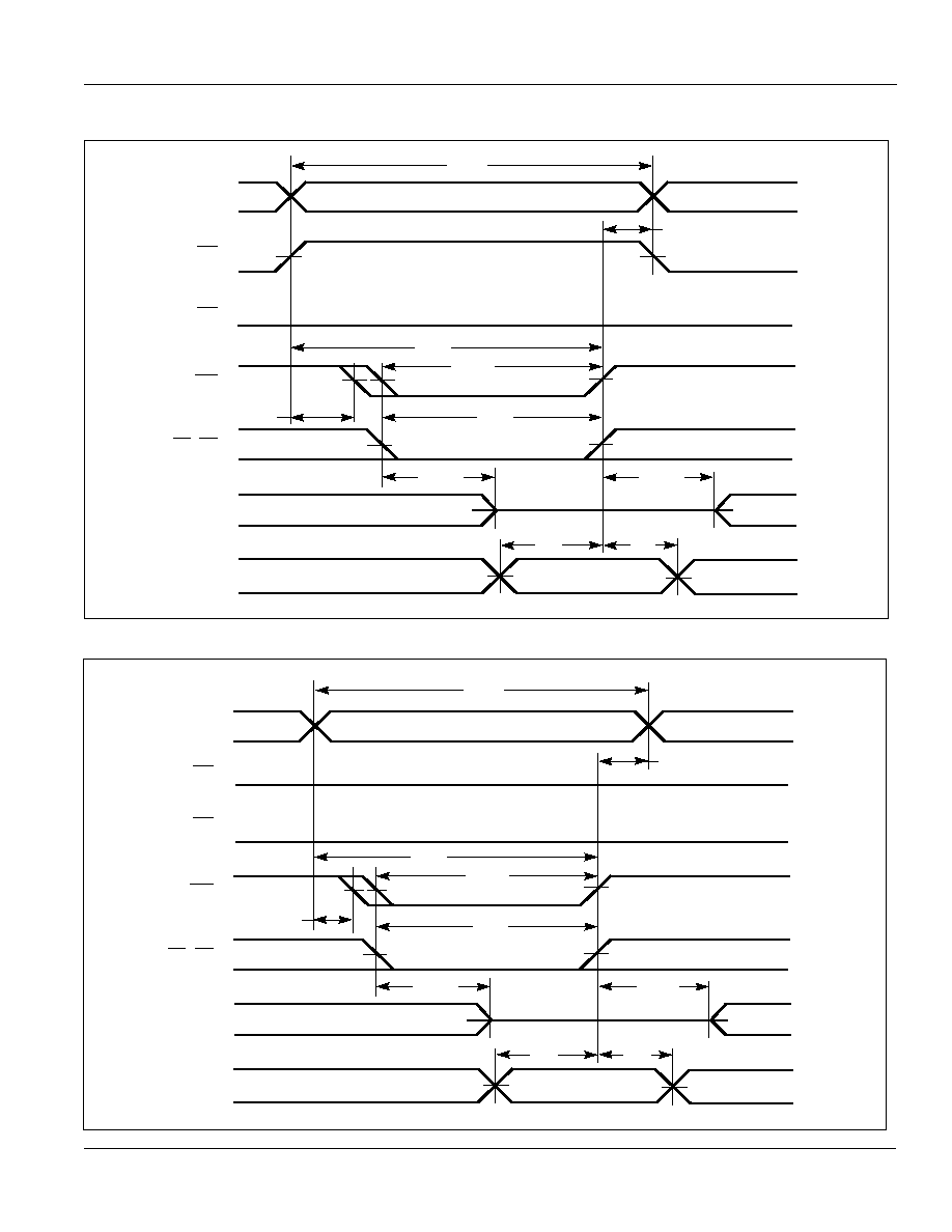
WRITE CYCLE NO. 3
(
WE Controlled: OE is LOW During Write Cycle)
DATA UNDEFINED
t
WC
VALID ADDRESS
LOW
LOW
t
PWE2
t
AW
t
HA
HIGH-Z
t
PBW
t
HD
t
SA
t
HZWE
ADDRESS
CE
UB, LB
WE
D
OUT
D
IN
OE
DATA
IN
VALID
t
LZWE
t
SD
UB_CEWR3.eps
IS61LV12816
10
Integrated Silicon Solution, Inc. -- 1-800-379-4774
Rev. A
11/30/00
ISSI
Æ
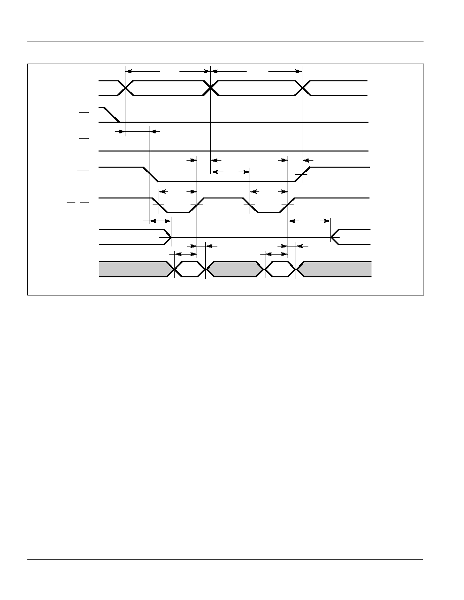
DATA UNDEFINED
t
WC
ADDRESS 1
ADDRESS 2
t
WC
HIGH-Z
t
PBW
WORD 1
LOW
WORD 2
UB_CEWR4.eps
t
HD
t
SA
t
HZWE
ADDRESS
CE
UB, LB
WE
D
OUT
D
IN
OE
DATA
IN
VALID
t
LZWE
t
SD
t
PBW
DATA
IN
VALID
t
SD
t
HD
t
SA
t
HA
t
HA
WRITE CYCLE NO. 4
(
LB, UB Controlled, Back-to-Back Write)
(1,3)
Notes:
1. The internal Write time is defined by the overlap of
CE = LOW, UB and/or LB = LOW, and WE = LOW. All signals must be
in valid states to initiate a Write, but any can be deasserted to terminate the Write. The
t
SA
,
t
HA
,
t
SD
, and
t
HD
timing is
referenced to the rising or falling edge of the signal that terminates the Write.
2. Tested with
OE HIGH for a minimum of 4 ns before WE = LOW to place the I/O in a HIGH-Z state.
3.
WE may be held LOW across many address cycles and the LB, UB pins can be used to control the Write function.
IS61LV12816
Integrated Silicon Solution, Inc. -- 1-800-379-4774
11
Rev. A
11/30/00
ISSI
Æ
IS61LV12816 STANDARD VERSION
ORDERING INFORMATION
Commercial Range: 0∞C to +70∞C
Speed (ns) Order Part No.
Package
8
IS61LV12816-8B
mini BGA (6mm x 8mm)
IS61LV12816-8K
400-mil Plastic SOJ
IS61LV12816-8LQ
LQFP
IS61LV12816-8T
Plastic TSOP
10
IS61LV12816-10B
mini BGA (6mm x 8mm)
IS61LV12816-10K
400-mil Plastic SOJ
IS61LV12816-10LQ
LQFP
IS61LV12816-10T
Plastic TSOP
12
IS61LV12816-12B
mini BGA (6mm x 8mm)
IS61LV12816-12K
400-mil Plastic SOJ
IS61LV12816-12LQ
LQFP
IS61LV12816-12T
Plastic TSOP
15
IS61LV12816-15B
mini BGA (6mm x 8mm)
IS61LV12816-15K
400-mil Plastic SOJ
IS61LV12816-15LQ
LQFP
IS61LV12816-15T
Plastic TSOP
IS61LV12816 STANDARD VERSION
ORDERING INFORMATION
Industrial Range: ≠40∞C to +85∞C
Speed (ns) Order Part No.
Package
8
IS61LV12816-8BI
mini BGA (6mm x 8mm)
IS61LV12816-8KI
400-mil Plastic SOJ
IS61LV12816-8LQI
LQFP
IS61LV12816-8TI
Plastic TSOP
10
IS61LV12816-10BI
mini BGA (6mm x 8mm)
IS61LV12816-10KI
400-mil Plastic SOJ
IS61LV12816-10LQI
LQFP
IS61LV12816-10TI
Plastic TSOP
12
IS61LV12816-12BI
mini BGA (6mm x 8mm)
IS61LV12816-12KI
400-mil Plastic SOJ
IS61LV12816-12LQI
LQFP
IS61LV12816-12TI
Plastic TSOP
15
IS61LV12816-15BI
mini BGA (6mm x 8mm)
IS61LV12816-15KI
400-mil Plastic SOJ
IS61LV12816-15LQI
LQFP
IS61LV12816-15TI
Plastic TSOP
ISSI
Æ
Integrated Silicon Solution, Inc.
2231 Lawson Lane
Santa Clara, CA 95054
Tel: 1-800-379-4774
Fax: (408) 588-0806
E-mail: sales@issi.com
www.issi.com