
Integrated Silicon Solution, Inc. -- 1-800-379-4774
1
Rev. A
03/17/06
IS61LV256AL
ISSI
Æ
Copyright © 2006 Integrated Silicon Solution, Inc. All rights reserved. ISSI reserves the right to make changes to this specification and its products at any time without notice. ISSI assumes no liability
arising out of the application or use of any information, products or services described herein. Customers are advised to obtain the latest version of this device specification before relying on any
published information and before placing orders for products.
FEATURES
∑ High-speed access times:
-- 10 ns
∑ Automatic power-down when chip is deselected
∑ CMOS low power operation
-- 60 µW (typical) CMOS standby
-- 65 mW (typical) operating
∑ TTL compatible interface levels
∑ Single 3.3V power supply
∑ Fully static operation: no clock or refresh
required
∑ Three-state outputs
∑ Lead-free available
DESCRIPTION
The
ISSI
IS61LV256AL is a very high-speed, low power,
32,768-word by 8-bit static RAM. It is fabricated using
ISSI
's high-performance CMOS technology. This highly
reliable process coupled with innovative circuit design
techniques, yields access times as fast as 8 ns maximum.
When
CE is HIGH (deselected), the device assumes a
standby mode at which the power dissipation is reduced to
150 µW (typical) with CMOS input levels.
Easy memory expansion is provided by using an active
LOW Chip Enable (
CE). The active LOW Write Enable
(
WE) controls both writing and reading of the memory.
The IS61LV256AL is available in the JEDEC standard 28-
pin, 300-mil SOJ and the 450-mil TSOP (Type I) packages.
32K x 8 LOW VOLTAGE
CMOS STATIC RAM
FUNCTIONAL BLOCK DIAGRAM
A0-A14
CE
OE
WE
32K X 8
MEMORY ARRAY
DECODER
COLUMN I/O
CONTROL
CIRCUIT
GND
VDD
I/O
DATA
CIRCUIT
I/O0-I/O7
MARCH 2006
IS61LV256AL
ISSI
Æ
2
Integrated Silicon Solution, Inc. -- 1-800-379-4774
Rev. A
03/17/06
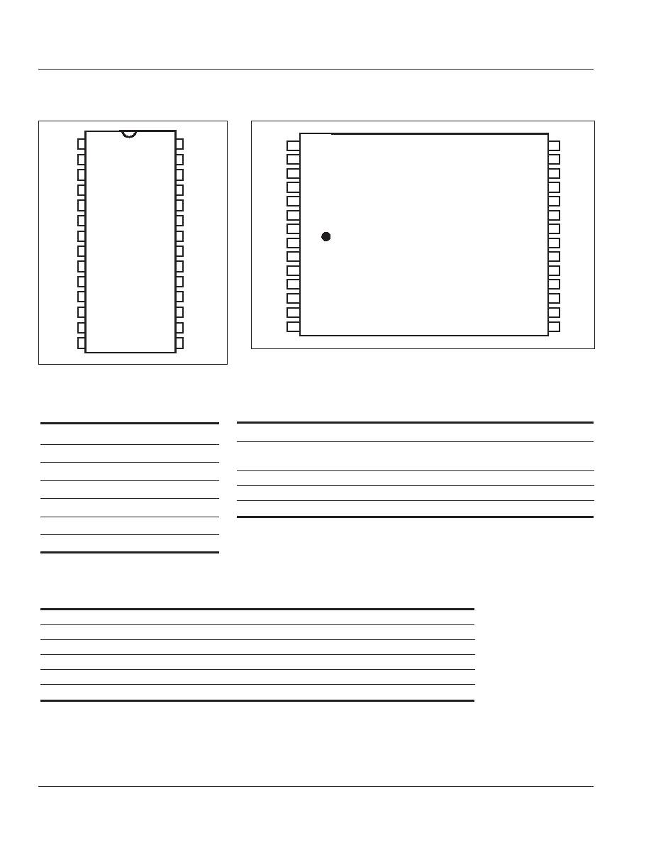
PIN CONFIGURATION
28-Pin SOJ
22
23
24
25
26
27
28
1
2
3
4
5
6
7
21
20
19
18
17
16
15
14
13
12
11
10
9
8
OE
A11
A9
A8
A13
WE
VDD
A14
A12
A7
A6
A5
A4
A3
A10
CE
I/O7
I/O6
I/O5
I/O4
I/O3
GND
I/O2
I/O1
I/O0
A0
A1
A2
1
2
3
4
5
6
7
8
9
10
11
12
13
14
28
27
26
25
24
23
22
21
20
19
18
17
16
15
A14
A12
A7
A6
A5
A4
A3
A2
A1
A0
I/O0
I/O1
I/O2
GND
VDD
WE
A13
A8
A9
A11
OE
A10
CE
I/O7
I/O6
I/O5
I/O4
I/O3
PIN CONFIGURATION
28-Pin TSOP (Type I)
PIN DESCRIPTIONS
A0-A14
Address Inputs
CE
Chip Enable Input
OE
Output Enable Input
WE
Write Enable Input
I/O0-I/O7
Input/Output
V
DD
Power
GND
Ground
TRUTH TABLE
Mode
WE
WE
WE
WE
WE
CE
CE
CE
CE
CE
OE
OE
OE
OE
OE
I/O Operation
V
DD
Current
Not Selected
X
H
X
High-Z
I
SB
1
, I
SB
2
(Power-down)
Output Disabled
H
L
H
High-Z
I
CC
Read
H
L
L
D
OUT
I
CC
Write
L
L
X
D
IN
I
CC
ABSOLUTE MAXIMUM RATINGS
(1)
Symbol
Parameter
Value
Unit
V
DD
Power Supply Voltage Relative to GND
≠0.5 to +4.6
V
V
TERM
Terminal Voltage with Respect to GND
≠0.5 to +4.6
V
T
STG
Storage Temperature
≠65 to +150
∞C
P
D
Power Dissipation
1
W
I
OUT
DC Output Current
±20
mA
Notes:
1. Stress greater than those listed under ABSOLUTE MAXIMUM RATINGS may cause permanent
damage to the device. This is a stress rating only and functional operation of the device at these or any
other conditions above those indicated in the operational sections of this specification is not implied.
Exposure to absolute maximum rating conditions for extended periods may affect reliability.
IS61LV256AL
ISSI
Æ
Integrated Silicon Solution, Inc. -- 1-800-379-4774
3
Rev. A
03/17/06
DC ELECTRICAL CHARACTERISTICS
(Over Operating Range)
Symbol Parameter
Test Conditions
Min.
Max.
Unit
V
OH
Output HIGH Voltage
V
DD
= Min., I
OH
= ≠2.0 mA
2.4
--
V
V
OL
Output LOW Voltage
V
DD
= Min., I
OL
= 4.0 mA
--
0.4
V
V
IH
Input HIGH Voltage
2.2
V
DD
+ 0.3
V
V
IL
Input LOW Voltage
(1)
≠0.3
0.8
V
I
LI
Input Leakage
GND
V
IN
V
DD
Com.
≠1
1
µA
Ind.
≠2
2
I
LO
Output Leakage
GND
V
OUT
V
DD
, Outputs Disabled
Com.
≠1
1
µA
Ind.
≠2
2
Notes:
1. V
IL
(min.) = ≠0.3V (DC); V
IL
(min.) = ≠2.0V (pulse width
2.0 ns).
V
IH
(max.) = V
DD
+ 0.5V (DC); V
IH
(max.) = V
DD
+ 2.0V (pulse width
2.0 ns).
2. Not more than one output should be shorted at one time. Duration of the short circuit should not exceed 30 seconds.
OPERATING RANGE
Range
Ambient Temperature
Speed (ns)
V
DD
(1)
Commercial
0∞C to +70∞C
10
3.3V, +10%, ≠5%
Industrial
≠40∞C to +85∞C
10
3.3V + 10%, ≠5%
Note: 1. If operated at 12ns, V
DD
range is 3.3V + 10%.

IS61LV256AL
ISSI
Æ
4
Integrated Silicon Solution, Inc. -- 1-800-379-4774
Rev. A
03/17/06
CAPACITANCE
(1,2)
Symbol
Parameter
Conditions
Max.
Unit
C
IN
Input Capacitance
V
IN
= 0V
6
pF
C
OUT
Output Capacitance
V
OUT
= 0V
5
pF
Notes:
1. Tested initially and after any design or process changes that may affect these parameters.
2. Test conditions: T
A
= 25∞C, f = 1 MHz, V
DD
= 3.3V.
POWER SUPPLY CHARACTERISTICS
(1)
(Over Operating Range)
-10 ns
Sym.
Parameter
Test Conditions
Min.
Max.
Unit
I
CC
1
V
DD
Operating
V
DD
= Max.,
CE = V
IL
Com.
--
20
mA
Supply Current
I
OUT
= 0 mA, f = 1 MHz
Ind.
--
25
I
CC
2
V
DD
Dynamic Operating
V
DD
= Max.,
CE = V
IL
Com.
--
30
mA
Supply Current
I
OUT
= 0 mA, f = f
MAX
Ind.
--
35
typ.
(2)
20
I
SB
1
TTL Standby Current
V
DD
= Max.,
Com.
--
1
mA
(TTL Inputs)
V
IN
= V
IH
or V
IL
Ind.
--
1
CE
V
IH
, f = 0
I
SB
2
CMOS Standby
V
DD
= Max.,
Com.
--
40
µA
Current (CMOS Inputs)
CE
V
DD
≠ 0.2V,
Ind.
--
50
V
IN
V
DD
≠ 0.2V, or
typ.
(2)
2
V
IN
0.2V, f = 0
Notes:
1. At f = f
MAX
, address and data inputs are cycling at the maximum frequency, f = 0 means no input lines change.
2. Typical values are measured at V
DD
= 3.3V, T
A
= 25
o
C and not 100% tested.
IS61LV256AL
ISSI
Æ
Integrated Silicon Solution, Inc. -- 1-800-379-4774
5
Rev. A
03/17/06
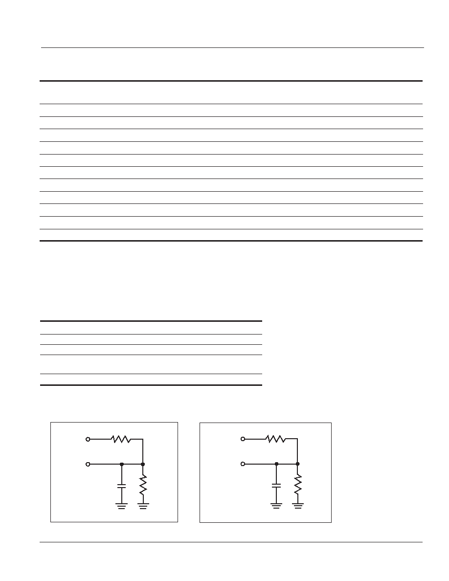
AC TEST LOADS
Figure 1.
Figure 2.
AC TEST CONDITIONS
Parameter
Unit
Input Pulse Level
0V to 3.0V
Input Rise and Fall Times
3 ns
Input and Output Timing
1.5V
and Reference Levels
Output Load
See Figures 1 and 2
READ CYCLE SWITCHING CHARACTERISTICS
(1)
(Over Operating Range)
-10 ns
-12 ns
Symbol
Parameter
Min.
Max.
Min.
Max.
Unit
t
RC
Read Cycle Time
10
--
12
--
ns
t
AA
Address Access Time
--
10
--
12
ns
t
OHA
Output Hold Time
2
--
2
--
ns
t
ACE
CE Access Time
--
10
--
12
ns
t
DOE
OE Access Time
--
5
--
5
ns
t
LZOE
(2)
OE to Low-Z Output
0
--
0
--
ns
t
HZOE
(2)
OE to High-Z Output
--
5
--
5
ns
t
LZCE
(2)
CE to Low-Z Output
3
--
3
--
ns
t
HZCE
(2)
CE to High-Z Output
--
5
--
6
ns
t
PU
(3)
CE to Power-Up
0
--
0
--
ns
t
PD
(3)
CE to Power-Down
--
10
--
12
ns
Notes:
1. Test conditions assume signal transition times of 3 ns or less, timing reference levels of 1.5V, input pulse levels of 0 to 3.0V
and output loading specified in Figure 1.
2. Tested with the load in Figure 2. Transition is measured ±200 mV from steady-state voltage. Not 100% tested.
3. Not 100% tested.
319
30 pF
Including
jig and
scope
353
OUTPUT
3.3V
319
5 pF
Including
jig and
scope
353
OUTPUT
3.3V
IS61LV256AL
ISSI
Æ
6
Integrated Silicon Solution, Inc. -- 1-800-379-4774
Rev. A
03/17/06
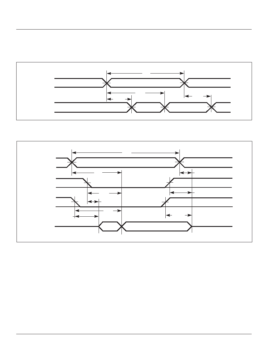
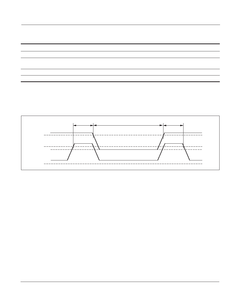
DATA VALID
READ1.eps
PREVIOUS DATA VALID
t
AA
t
OHA
t
OHA
t
RC
D
OUT
ADDRESS
t
RC
t
OHA
t
AA
t
DOE
t
LZOE
t
ACE
t
LZCE
t
HZOE
HIGH-Z
DATA VALID
CE_RD2.eps
ADDRESS
OE
CE
D
OUT
t
HZCE
READ CYCLE NO. 2
(1,3)
Notes:
1.
WE is HIGH for a Read Cycle.
2. The device is continuously selected.
OE, CE = V
IL
.
3. Address is valid prior to or coincident with
CE LOW transitions.
AC WAVEFORMS
READ CYCLE NO. 1
(1,2)

IS61LV256AL
ISSI
Æ
Integrated Silicon Solution, Inc. -- 1-800-379-4774
7
Rev. A
03/17/06
AC WAVEFORMS
WRITE CYCLE NO. 1
(
CE Controlled, OE is HIGH or LOW)
(1 )
DATA UNDEFINED
t
WC
VALID ADDRESS
t
SCE
t
PWE1
t
PWE2
t
AW
t
HA
HIGH-Z
t
HD
t
SA
t
HZWE
ADDRESS
CE
WE
D
OUT
D
IN
DATA
IN
VALID
t
LZWE
t
SD
CE_WR1.eps
WRITE CYCLE SWITCHING CHARACTERISTICS
(1,2)
(Over Operating Range)
-10 ns
-12 ns
Symbol
Parameter
Min.
Max.
Min. Max.
Unit
t
WC
Write Cycle Time
10
--
12
--
ns
t
SCE
CE to Write End
8
--
8
--
ns
t
AW
Address Setup Time
8
--
8
--
ns
to Write End
t
HA
Address Hold
0
--
0
--
ns
from Write End
t
SA
Address Setup Time
0
--
0
--
ns
t
PWE
1
WE Pulse Width (OE HIGH)
7
--
8
--
ns
t
PWE
2
WE Pulse Width (OE LOW)
10
--
12
--
ns
t
SD
Data Setup to Write End
6.5
--
7
--
ns
t
HD
Data Hold from Write End
0
--
0
--
ns
t
HZWE
(3)
WE LOW to High-Z Output
--
3.5
--
5
ns
t
LZWE
(3)
WE HIGH to Low-Z Output
0
--
0
--
ns
Notes:
1. Test conditions assume signal transition times of 3 ns or less, timing reference levels of 1.5V, input pulse levels of 0 to 3.0V
and output loading specified in Figure 1.
2. The internal write time is defined by the overlap of
CE LOW and WE LOW. All signals must be in valid states to initiate a
Write, but any one can go inactive to terminate the Write. The Data Input Setup and Hold timing are referenced to the rising
or falling edge of the signal that terminates the Write.
3. Tested with the load in Figure 2. Transition is measured ±500 mV from steady-state voltage. Not 100% tested.

IS61LV256AL
ISSI
Æ
8
Integrated Silicon Solution, Inc. -- 1-800-379-4774
Rev. A
03/17/06
DATA UNDEFINED
LOW
t
WC
VALID ADDRESS
t
PWE1
t
AW
t
HA
HIGH-Z
t
HD
t
SA
t
HZWE
ADDRESS
CE
WE
D
OUT
D
IN
OE
DATA
IN
VALID
t
LZWE
t
SD
CE_WR2.eps
WRITE CYCLE NO. 2
(
WE Controlled, OE is HIGH During Write Cycle)
(1,2)
WRITE CYCLE NO. 3
(
WE Controlled, OE is LOW During Write Cycle)
(1)
DATA UNDEFINED
t
WC
VALID ADDRESS
LOW
LOW
t
PWE2
t
AW
t
HA
HIGH-Z
t
HD
t
SA
t
HZWE
ADDRESS
CE
WE
D
OUT
D
IN
OE
DATA
IN
VALID
t
LZWE
t
SD
CE_WR3.eps
Notes:
1. The internal write time is defined by the overlap of
CE LOW and WE LOW. All signals must be in valid states to initiate a Write,
but any one can go inactive to terminate the Write. The Data Input Setup and Hold timing are referenced to the rising or falling
edge of the signal that terminates the Write.
2. I/O will assume the High-Z state if
OE
> V
IH
.
IS61LV256AL
ISSI
Æ
Integrated Silicon Solution, Inc. -- 1-800-379-4774
9
Rev. A
03/17/06
DATA RETENTION SWITCHING CHARACTERISTICS
Symbol
Parameter
Test Condition
Min.
Typ.
(1)
Max.
Unit
V
DR
V
DD
for Data Retention
See Data Retention Waveform
2.0
3.6
V
I
DR
Data Retention Current
V
DD
= 2.0V,
CE
V
DD
≠ 0.2V
Com.
--
2
40
µA
V
IN
V
DD
≠ 0.2V, or V
IN
V
SS
+ 0.2V
Ind.
--
--
50
t
SDR
Data Retention Setup Time
See Data Retention Waveform
0
--
ns
t
RDR
Recovery Time
See Data Retention Waveform
t
RC
--
ns
Note:
1. Typical Values are measured at V
DD
= 3.3V, T
A
= 25
o
C and not 100% tested.
DATA RETENTION WAVEFORM (
CE
CE
CE
CE
CE Controlled)
VDD
CE
VDD
- 0.2V
t
SDR
t
RDR
V
DR
CE
GND
Data Retention Mode

IS61LV256AL
ISSI
Æ
10
Integrated Silicon Solution, Inc. -- 1-800-379-4774
Rev. A
03/17/06
ORDERING INFORMATION
Commercial Range: 0∞C to +70∞C
Speed (ns)
Order Part No.
Package
10
IS61LV256AL-10T
TSOP - Type I
IS61LV256AL-10TL
TSOP - Type I, Lead-free
IS61LV256AL-10J
300-mil Plastic SOJ
IS61LV256AL-10JL
300-mil Plastic SOJ, Lead-free
ORDERING INFORMATION
Industrial Range: ≠40∞C to +85∞C
Speed (ns)
Order Part No.
Package
10
IS61LV256AL-10TI
TSOP - Type I
IS61LV256AL-10TLI
TSOP - Type I, Lead-free
IS61LV256AL-10JI
300-mil Plastic SOJ
IS61LV256AL-10JLI
300-mil Plastic SOJ, Lead-free

PACKAGING INFORMATION
ISSI
Æ
Integrated Silicon Solution, Inc. -- www.issi.com --
1-800-379-4774
Rev. D
02/25/03
Copyright © 2003 Integrated Silicon Solution, Inc. All rights reserved. ISSI reserves the right to make changes to this specification and its products at any time
without notice. ISSI assumes no liability arising out of the application or use of any information, products or services described herein. Customers are advised to
obtain the latest version of this device specification before relying on any published information and before placing orders for products.
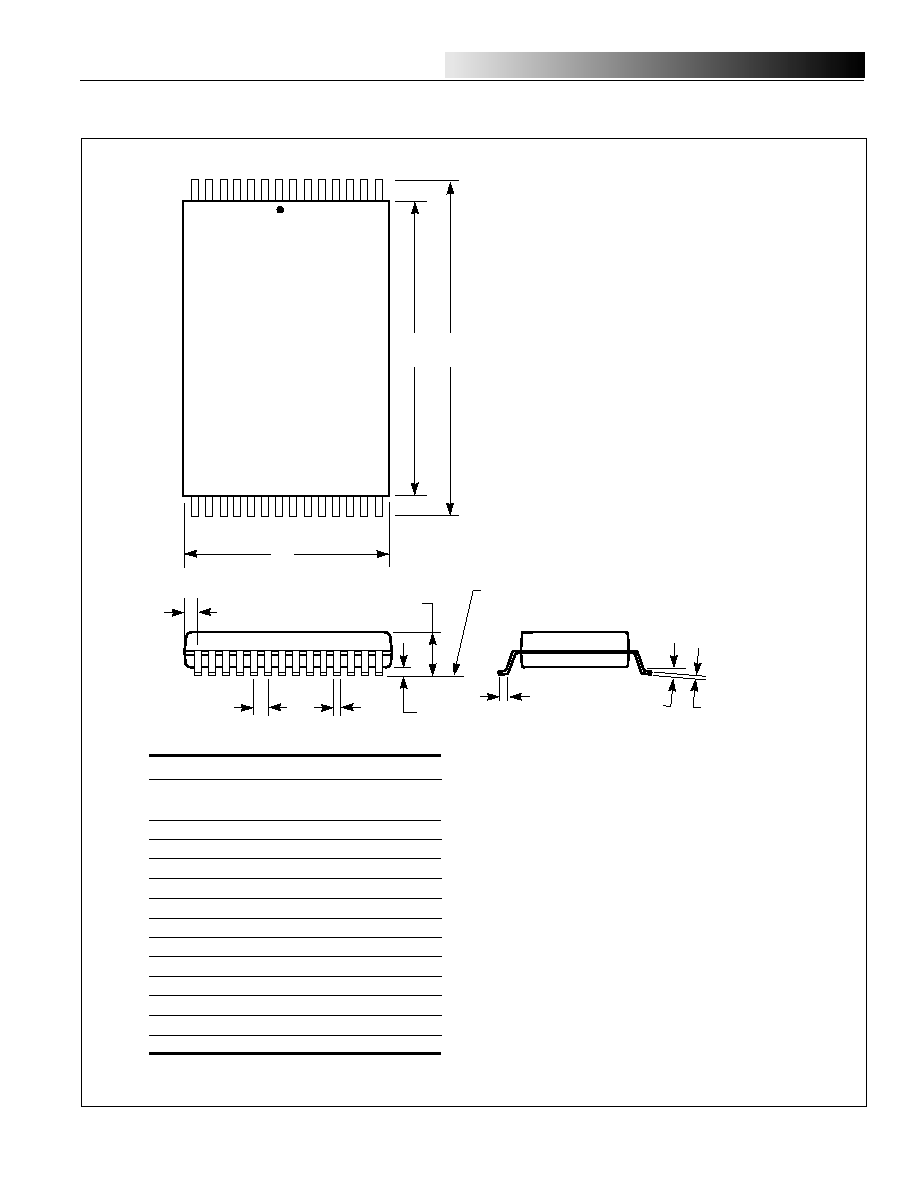
300-mil Plastic SOJ
Package Code: J
Notes:
1. Controlling dimension: inches, unless otherwise
specified.
2. BSC = Basic lead spacing between centers.
3. Dimensions D and E1 do not include mold flash
protrusions and
should be measured from the bottom of
the package
.
4. Formed leads shall be planar with respect to one
another within 0.004 inches at the seating plane.
MILLIMETERS
INCHES
Sym.
Min. Typ. Max.
Min. Typ. Max.
N0.
Leads
24/26
A
--
--
3.56
--
--
0.140
A1
0.64
--
--
0.025
--
--
A2
2.41
--
2.67
0.095
--
0.105
b
0.41
--
0.51
0.016
--
0.020
B
0.66
--
0.81
0.026
--
0.032
C
0.20
--
0.25
0.008
--
0.010
D
17.02
--
17.27
0.670
--
0.680
E
8.26
--
8.76
0.325
--
0.345
E1
7.49
--
7.75
0.295
--
0.305
E2
6.27
--
7.29
0.247
--
0.287
e
1.27 BSC
0.050 BSC
SEATING PLANE
1
N
E1
D
E2
E
b
e
A1
A
B
C
A2
PACKAGING INFORMATION
ISSI
Æ
2
Integrated Silicon Solution, Inc. -- www.issi.com --
1-800-379-4774
Rev. D
02/25/03
MILLIMETERS
INCHES
Sym.
Min. Typ. Max.
Min. Typ. Max.
N0.
Leads
28
A
--
--
3.56
--
--
0.140
A1
0.64
--
--
0.025
--
--
A2
2.41
--
2.67
0.095
--
0.105
b
0.41
--
0.51
0.016
--
0.020
B
0.66
--
0.81
0.026
--
0.032
C
0.20
--
0.25
0.008
--
0.010
D
18.29
--
18.54
0.720
--
0.730
E
8.26
--
8.76
0.325
--
0.345
E1
7.49
--
7.75
0.295
--
0.305
E2
6.27
--
7.29
0.247
--
0.287
e
1.27 BSC
0.050 BSC
MILLIMETERS
INCHES
Sym.
Min. Typ. Max.
Min. Typ. Max.
N0.
Leads
32
A
--
--
3.56
--
--
0.140
A1
0.64
--
--
0.025
--
--
A2
2.41
--
2.67
0.095
--
0.105
b
0.41
--
0.51
0.016
--
0.020
B
0.66
--
0.81
0.026
--
0.032
C
0.20
--
0.25
0.008
--
0.010
D
20.83
--
21.08
0.820
--
0.830
E
8.26
--
8.76
0.325
--
0.345
E1
7.49
--
7.75
0.295
--
0.305
E2
6.27
--
7.29
0.247
--
0.287
e
1.27 BSC
0.050 BSC
300-mil Plastic SOJ
Package Code: J
Integrated Silicon Solution, Inc.
ISSI
Æ
PACKAGING INFORMATION
D
SEATING PLANE
B
e
C
1
E
A1
A
S
H
L
N
Plastic TSOP - 28-pins
Package Code: T (Type I)
Plastic TSOP (T--Type I)
Millimeters
Inches
Symbol
Min
Max
Min
Max
Ref. Std.
No. Leads
28
A
1.00
1.20
0.037
0.047
A1
0.05
0.20
0.002
0.008
B
0.16
0.27
0.006
0.011
C
0.10
0.20
0.004
0.008
D
7.90
8.10
0.308
0.316
E
11.70
11.90
0.456
0.465
H
13.20
13.60
0.515
0.531
e
0.55 BSC
0.022 BSC
L
0.30
0.70
0.011
0.027
0
∞
5
∞
0
∞
5
∞
Notes:
1. Controlling dimension: millimeters, unless otherwise specified.
2. BSC = Basic lead spacing between centers.
3. Dimensions D and E do not include mold flash protrusions and
should be measured from the bottom of the package
.
4. Formed leads shall be planar with respect to one another within
0.004 inches at the seating plane.
PK13197T28 Rev. B 01/31/97