IS61LV6464
ISSI
Æ
Integrated Silicon Solution, Inc. -- 1-800-379-4774
1
Rev. A
04/17/01
ISSI reserves the right to make changes to its products at any time without notice in order to improve design and supply the best possible product. We assume no responsibility for any
errors which may appear in this publication. © Copyright 2001, Integrated Silicon Solution, Inc.
FEATURES
∑ Fast access time:
≠ -100 MHz; 6 ns-83 MHz;
7 ns-75 MHz; 8 ns-66 MHz
∑ Internal self-timed write cycle
∑ Individual Byte Write Control and Global Write
∑ Clock controlled, registered address, data and
control
∑ PentiumTM or linear burst sequence control
using MODE input
∑ Five chip enables for simple depth expansion
and address pipelining
∑ Common data inputs and data outputs
∑ Power-down control by ZZ input
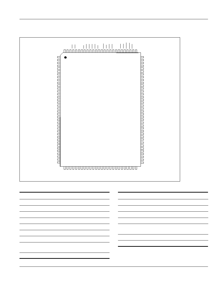
∑ JEDEC 128-Pin TQFP 14mm x 20mm
package
∑ Single +3.3V power supply
∑ 2.5V V
CCQ
(I/O supply)
∑ Control pins mode upon power-up:
≠ MODE in interleave burst mode
≠ ZZ in normal operation mode
These control pins can be connected to GND
Q
or V
CCQ
to alter their power-up state
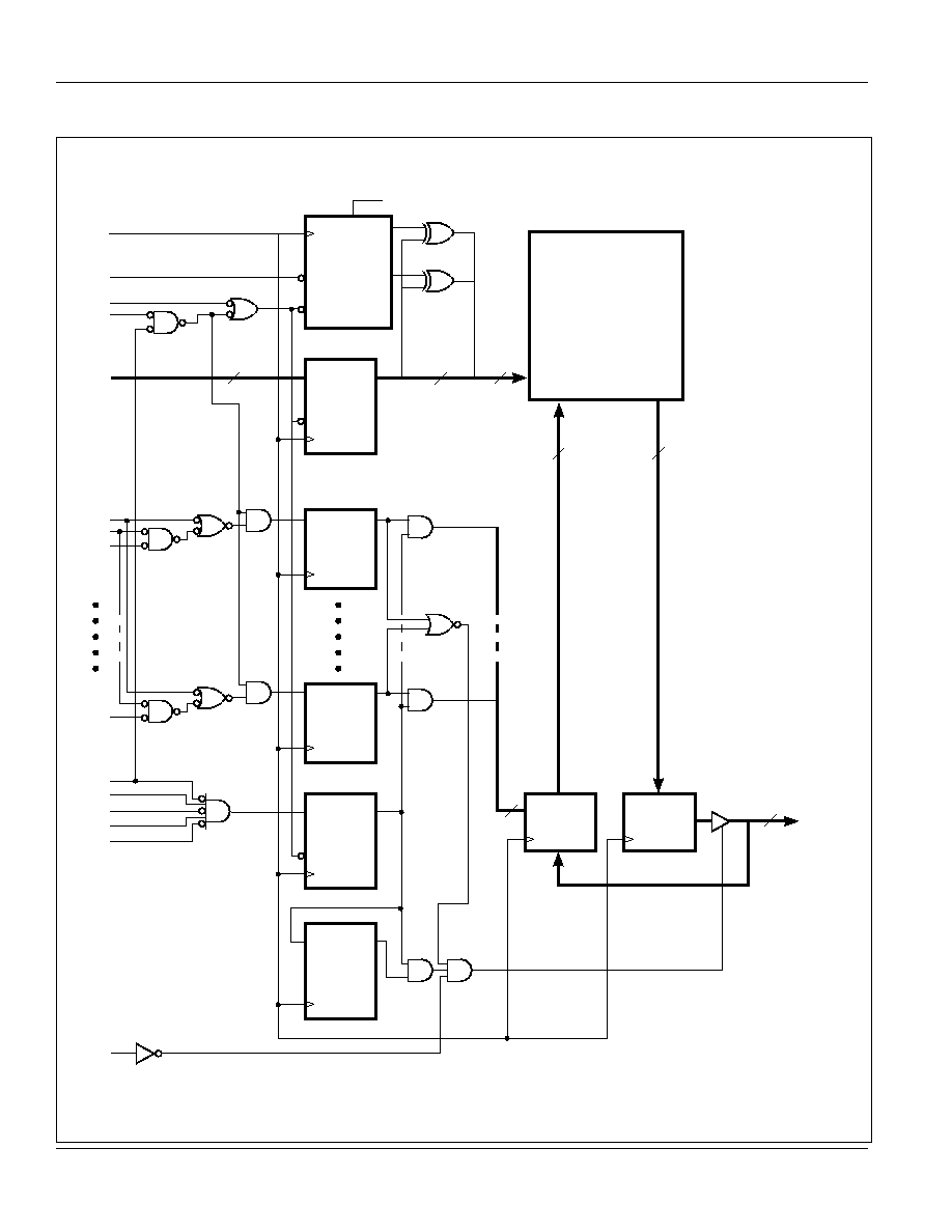
DESCRIPTION
The
ISSI
IS61LV6464 is a high-speed, low-power synchro-
nous static RAM designed to provide a burstable, high-
performance, secondary cache for the PentiumTM, 680X0TM,
and PowerPCTM microprocessors. It is organized as 65,536
words by 64 bits, fabricated with
ISSI
's advanced CMOS
technology. The device integrates a 2-bit burst counter, high-
speed SRAM core, and high-drive capability outputs into a
single monolithic circuit. All synchronous inputs pass through
registers controlled by a positive-edge-triggered single clock
input.
Write cycles are internally self-timed and are initiated by the
rising edge of the clock input. Write cycles can be from one to
eight bytes wide as controlled by the write control inputs.
Separate byte enables allow individual bytes to be written.
BW1
controls I/O1-I/O8,
BW2
controls I/O9-I/O16,
BW3
con-
trols I/O17-I/O24,
BW4
controls I/O25-I/O32,
BW5
controls
I/O33-I/O40,
BW6
controls I/O41-I/O48,
BW7
controls I/O49-
I/O56,
BW8
controls I/O57-I/O64, conditioned by
BWE
being
LOW. A LOW on
GW
input would cause all bytes to be written.
Bursts can be initiated with either
ADSP
(Address Status
Processor) or
ADSC
(Address Status Cache Controller) input
pins. Subsequent burst addresses can be generated inter-
nally by the IS61LV6464 and controlled by the
ADV
(burst
address advance) input pin.
Asynchronous signals include output enable (
OE
), sleep mode
input (ZZ), and burst mode input (MODE). A HIGH input on the
ZZ pin puts the SRAM in the power-down state. When ZZ is
pulled LOW (or no connect), the SRAM normally operates
after the wake-up period. A LOW input, i.e., GND
Q
, on MODE
pin selects LINEAR Burst. A V
CCQ
(or no connect) on MODE
pin selects INTERLEAVED Burst.
64K x 64 SYNCHRONOUS
PIPELINE STATIC RAM
APRIL 2001

IS61LV6464
ISSI
Æ
4
Integrated Silicon Solution, Inc. -- 1-800-379-4774
Rev. A
04/17/01
TRUTH TABLE
ADDRESS
OPERATION
USED
CE3
CE2
CE3
CE2
CE
ADSP ADSC ADV WRITE
OE
CLK
I/O
Deselected, Power-down
None
X
X
X
X
H
X
L
X
X
X
L-H
High-Z
Deselected, Power-down
None
L
X
X
X
L
L
X
X
X
X
L-H
High-Z
Deselected, Power-down
None
X
L
X
X
L
L
X
X
X
X
L-H
High-Z
Deselected, Power-down
None
X
X
H
X
L
L
X
X
X
X
L-H
High-Z
Deselected, Power-down
None
X
X
X
H
L
L
X
X
X
X
L-H
High-Z
Deselected, Power-down
None
L
X
X
X
L
H
L
X
X
X
L-H
High-Z
Deselected, Power-down
None
X
L
X
X
L
H
L
X
X
X
L-H
High-Z
Deselected, Power-down
None
X
X
H
X
L
H
L
X
X
X
L-H
High-Z
Deselected, Power-down
None
X
X
X
H
L
H
L
X
X
X
L-H
High-Z
Read Cycle, Begin Burst
External
H
H
L
L
L
L
X
X
X
L
L-H
Dout
Read Cycle, Begin Burst
External
H
H
L
L
L
L
X
X
X
H
L-H
High-Z
Write Cycle, Begin Burst
External
H
H
L
L
L
H
L
X
L
X
L-H
Din
Read Cycle, Begin Burst
External
H
H
L
L
L
H
L
X
H
L
L-H
Dout
Read Cycle, Begin Burst
External
H
H
L
L
L
H
L
X
H
H
L-H
High-Z
Read Cycle, Continue Burst
Next
X
X
X
X
X
H
H
L
H
L
L-H
Dout
Read Cycle, Continue Burst
Next
X
X
X
X
X
H
H
L
H
H
L-H
High-Z
Read Cycle, Continue Burst
Next
X
X
X
X
H
X
H
L
H
L
L-H
Dout
Read Cycle, Continue Burst
Next
X
X
X
X
H
X
H
L
H
H
L-H
High-Z
Write Cycle, Continue Burst
Next
X
X
X
X
X
H
H
L
L
X
L-H
Din
Write Cycle, Continue Burst
Next
X
X
X
X
H
X
H
L
L
X
L-H
Din
Read Cycle, Suspend Burst
Current
X
X
X
X
X
H
H
H
H
L
L-H
Dout
Read Cycle, Suspend Burst
Current
X
X
X
X
X
H
H
H
H
H
L-H
High-Z
Read Cycle, Suspend Burst
Current
X
X
X
X
H
X
H
H
H
L
L-H
Dout
Read Cycle, Suspend Burst
Current
X
X
X
X
H
X
H
H
H
H
L-H
High-Z
Write Cycle, Suspend Burst
Current
X
X
X
X
X
H
H
H
L
X
L-H
Din
Write Cycle, Suspend Burst
Current
X
X
X
X
H
X
H
H
L
X
L-H
Din
Notes:
1. All inputs except
OE
must meet setup and hold times for the Low-to-High transition of clock (CLK).
2. Wait states are inserted by suspending burst.
3. X means don't care.
WRITE
=L means any one or more byte write enable signals (
BW
1-
BW
8) and
BWE
are LOW or
GW
is LOW.
WRITE
=H means all byte write enable signals are HIGH.
4. For a Write operation following a Read operation,
OE
must be HIGH before the input data required setup time and held HIGH
throughout the input data hold time.
5.
ADSP
LOW always initiates an internal READ at the Low-to-High edge of clock. A WRITE is performed by setting one or more
byte write enable signals and
BWE
LOW or
GW
LOW for the subsequent L-H edge of clock.