Integrated Silicon Solution, Inc. -- www.issi.com --
1-800-379-4774
1
Rev. 00A
08/26/05
IS61NLF12836A/IS61NVF12836A
IS61NLF25618A/IS61NVF25618A
ISSI
Æ
Copyright © 2005 Integrated Silicon Solution, Inc. All rights reserved. ISSI reserves the right to make changes to this specification and its products at any time without notice. ISSI assumes no liability
arising out of the application or use of any information, products or services described herein. Customers are advised to obtain the latest version of this device specification before relying on any
published information and before placing orders for products.
FEATURES
∑ 100 percent bus utilization
∑ No wait cycles between Read and Write
∑ Internal self-timed write cycle
∑ Individual Byte Write Control
∑ Single Read/Write control pin
∑ Clock controlled, registered address,
data and control
∑ Interleaved or linear burst sequence control using
MODE input
∑ Three chip enables for simple depth expansion
and address pipelining
∑ Power Down mode
∑ Common data inputs and data outputs
∑
CKE
pin to enable clock and suspend operation
∑ JEDEC 100-pin TQFP, 119-ball PBGA, and 165-
ball PBGA packages
∑ Power supply:
NVF: V
DD
2.5V (± 5%), V
DDQ
2.5V (± 5%)
NLF: V
DD
3.3V (± 5%), V
DDQ
3.3V/2.5V (± 5%)
∑ Industrial temperature available
∑ Lead-free available
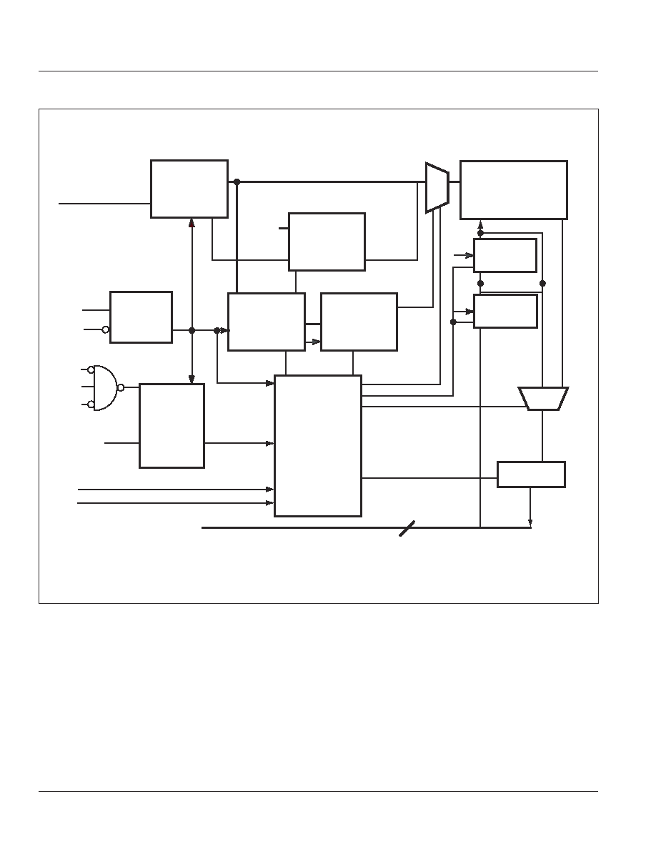
DESCRIPTION
The 4 Meg 'NLF/NVF' product family feature high-speed,
low-power synchronous static RAMs designed to provide
a burstable, high-performance, 'no wait' state, device for
networking and communications applications. They are
organized as 128K words by 36 bits and 256K words by 18
bits, fabricated with
ISSI
's advanced CMOS technology.
Incorporating a 'no wait' state feature, wait cycles are
eliminated when the bus switches from read to write, or
write to read. This device integrates a 2-bit burst counter,
high-speed SRAM core, and high-drive capability outputs
into a single monolithic circuit.
All synchronous inputs pass through registers are controlled
by a positive-edge-triggered single clock input. Operations
may be suspended and all synchronous inputs ignored
when Clock Enable,
CKE
is HIGH. In this state the internal
device will hold their previous values.
All Read, Write and Deselect cycles are initiated by the
ADV input. When the ADV is HIGH the internal burst
counter is incremented. New external addresses can be
loaded when ADV is LOW.
Write cycles are internally self-timed and are initiated by
the rising edge of the clock inputs and when
WE
is LOW.
Separate byte enables allow individual bytes to be written.
A burst mode pin (MODE) defines the order of the burst
sequence. When tied HIGH, the interleaved burst sequence
is selected. When tied LOW, the linear burst sequence is
selected.
128K x 36 and 256K x 18
4Mb, FLOW THROUGH 'NO WAIT'
STATE BUS SRAM
PRELIMINARY INFORMATION
SEPTEMBER 2005
FAST ACCESS TIME
Symbol
Parameter
6.5
7.5
Units
t
KQ
Clock Access Time
6.5
7.5
ns
t
KC
Cycle Time
7.5
8.5
ns
Frequency
133
117
MHz
4
Integrated Silicon Solution, Inc. -- www.issi.com --
1-800-379-4774
Rev. 00A
08/26/05
IS61NLF12836A/IS61NVF12836A
IS61NLF25618A/IS61NVF25618A
ISSI
Æ
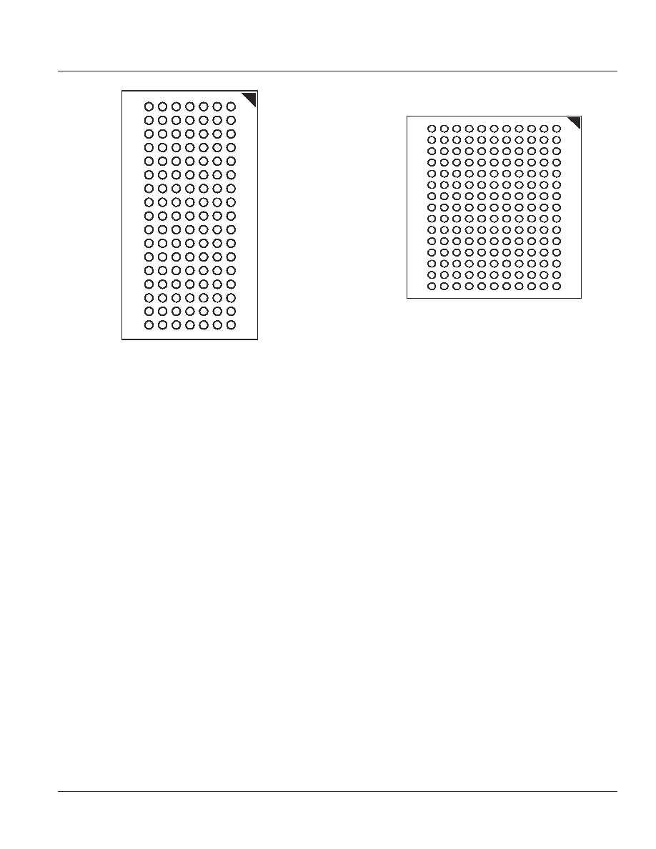
PIN CONFIGURATION -- 128K
X
36, 165-Ball PBGA (TOP VIEW)
1
2
3
4
5
6
7
8
9
10
11
A
NC
A
CE
BW
c
BW
b
CE
2
CKE
ADV
NC
A
NC
B
NC
A
CE2
BW
d
BW
a
CLK
WE
OE
NC
A
NC
C
DQPc
NC
V
DDQ
V
SS
V
SS
V
SS
V
SS
V
SS
V
DDQ
NC
DQPb
D
DQc
DQc
V
DDQ
V
DD
V
SS
V
SS
V
SS
V
DD
V
DDQ
DQb
DQb
E
DQc
DQc
V
DDQ
V
DD
V
SS
V
SS
V
SS
V
DD
V
DDQ
DQb
DQb
F
DQc
DQc
V
DDQ
V
DD
V
SS
V
SS
V
SS
V
DD
V
DDQ
DQb
DQb
G
DQc
DQc
V
DDQ
V
DD
V
SS
V
SS
V
SS
V
DD
V
DDQ
DQb
DQb
H
NC
NC
NC
V
DD
V
SS
V
SS
V
SS
V
DD
NC
NC
ZZ
J
DQd
DQd
V
DDQ
V
DD
V
SS
V
SS
V
SS
V
DD
V
DDQ
DQa
DQa
K
DQd
DQd
V
DDQ
V
DD
V
SS
V
SS
V
SS
V
DD
V
DDQ
DQa
DQa
L
DQd
DQd
V
DDQ
V
DD
V
SS
V
SS
V
SS
V
DD
V
DDQ
DQa
DQa
M
DQd
DQd
V
DDQ
V
DD
V
SS
V
SS
V
SS
V
DD
V
DDQ
DQa
DQa
N
DQPd
NC
V
DDQ
V
SS
NC
NC
NC
V
SS
V
DDQ
NC
DQPa
P
NC
NC
A
A
NC
A1*
NC
A
A
A
NC
R
MODE
NC
A
A
NC
A0*
NC
A
A
A
A
Note:
A0 and A1 are the two least significant bits (LSB) of the address field and set the internal burst counter if burst is desired.
PIN DESCRIPTIONS
Symbol
Pin Name
A
Address Inputs
A0, A1
Synchronous Burst Address Inputs
ADV
Synchronous Burst Address Advance/
Load
WE
Synchronous Read/Write Control Input
CLK
Synchronous Clock
CKE
Clock Enable
CE
,
CE2
, CE2 Synchronous Chip Enable
BW
x (x=a-d)
Synchronous Byte Write Inputs
OE
Output Enable
ZZ
Power Sleep Mode
MODE
Burst Sequence Selection
V
DD
3.3V/2.5V Power Supply
NC
No Connect
DQx
Data Inputs/Outputs
DQPx
Parity Data I/O
V
DDQ
Isolated output Power Supply
3.3V/2.5V
V
SS
Ground
Integrated Silicon Solution, Inc. -- www.issi.com --
1-800-379-4774
5
Rev. 00A
08/26/05
IS61NLF12836A/IS61NVF12836A
IS61NLF25618A/IS61NVF25618A
ISSI
Æ
119-PIN PBGA PACKAGE CONFIGURATION 128K x 36 (TOP VIEW)
1
2
3
4
5
6
7
A
A
BW
b
B
NC
C
NC
D
DQc
DQPc
Vss
E
DQc
DQc
Vss
F
V
DDQ
DQc
G
DQc
DQc
H
DQc
DQc
J
V
DDQ
V
DD
K
DQd
DQd
L
DQd
DQd
M
V
DDQ
DQd
N
DQd
DQd
Vss
P
NC
DQPd
R
A
CE2
MODE
A
0
*
A
A
A
V
SS
V
SS
V
SS
V
SS
BW
d
V
SS
V
SS
V
SS
NC
NC
V
DD
V
DD
V
DD
V
DD
NC
Vss
Vss
Vss
Vss
Vss
NC
CE
2
NC
A
NC
T
U
V
DDQ
NC
V
DDQ
DQd
A
NC
NC
NC
A
A
BW
c
NC
A
1
*
CKE
NC
CLK
NC
WE
NC
OE
CE
NC
ADV
NC
A
NC
BW
a
A
A
A
DQPa
DQa
DQa
DQa
DQa
DQb
DQb
DQb
DQb
DQPb
A
A
V
DDQ
ZZ
DQa
DQa
V
DDQ
DQa
DQa
V
DDQ
DQb
DQb
V
DDQ
DQb
DQb
NC
V
DDQ
V
SS
Note:
A0 and A1 are the two least significant bits (LSB) of the address field and set the internal burst counter if burst is desired.
PIN DESCRIPTIONS
Symbol
Pin Name
A
Address Inputs
A0, A1
Synchronous Burst Address Inputs
ADV
Synchronous Burst Address Advance/
Load
WE
Synchronous Read/Write Control Input
CLK
Synchronous Clock
CKE
Clock Enable
CE
Synchronous Chip Select
CE
2
Synchronous Chip Select
CE2
Synchronous Chip Select
BW
x (x=a-d)
Synchronous Byte Write Inputs
OE
Output Enable
ZZ
Power Sleep Mode
MODE
Burst Sequence Selection
V
DD
Power Supply
V
SS
Ground
NC
No Connect
DQa-DQd
Data Inputs/Outputs
DQPa-Pd
Parity Data I/O
V
DDQ
Output Power Supply