Integrated Silicon Solution, Inc. -- www.issi.com --
1-800-379-4774
1
ADVANCED INFORMATION Rev. 00A
07/17/02
IS61NVVP25672
IS61NVVP51236
ISSI
Æ
Copyright © 2002 Integrated Silicon Solution, Inc. All rights reserved. ISSI reserves the right to make changes to this specification and its products at any time
without notice. ISSI assumes no liability arising out of the application or use of any information, products or services described herein. Customers are advised to
obtain the latest version of this device specification before relying on any published information and before placing orders for products.
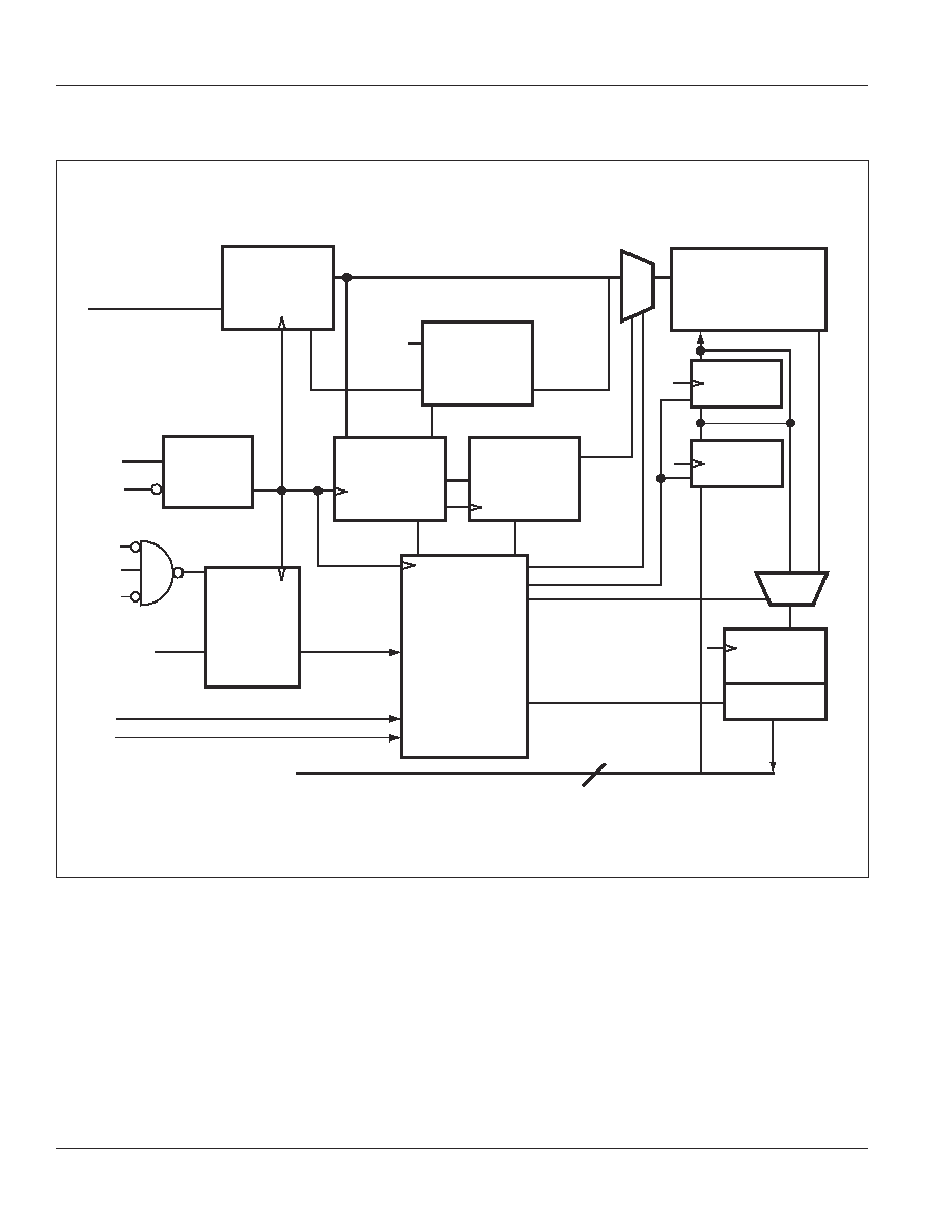
FEATURES
∑ 100 percent bus utilization
∑ No wait cycles between Read and Write
∑ Internal self-timed write cycle
∑ Individual Byte Write Control
∑ Single R/W (Read/Write) control pin
∑ Clock controlled, registered address,
data and control
∑ Interleaved or linear burst sequence control
using MODE input
∑ Power Down mode
∑ Common data inputs and data outputs
∑
CKE
pin to enable clock and suspend operation
∑ JEDEC 119-ball PBGA (x36) and
209-ball (x72) PBGA packages
∑ Single +1.8V (± 5%) power supply
∑ JTAG Boundary Scan
∑ Industrial temperature available
DESCRIPTION
The 16 Meg 'NVVP' product family feature high-speed,
low-power synchronous static RAMs designed to provide
a burstable, high-performance, 'no wait' state, device for
network and communications customers. They are
organized as 256K words by 72 bits, 512K words
by 36 bits and are fabricated with
ISSI
's advanced CMOS
technology.
Incorporating a 'no wait' state feature, wait cycles are
eliminated when the bus switches from read to write, or
write to read. This device integrates a 2-bit burst counter,
high-speed SRAM core, and high-drive capability outputs
into a single monolithic circuit.
All synchronous inputs pass through registers are controlled
by a positive-edge-triggered single clock input. Operations
may be suspended and all synchronous inputs ignored
when Clock Enable,
CKE
is HIGH. In this state the internal
device will hold their previous values.
All Read, Write and Deselect cycles are initiated by the
ADV input. When the ADV is HIGH the internal burst
counter is incremented. New external addresses can be
loaded when ADV is LOW.
Write cycles are internally self-timed and are initiated by
the rising edge of the clock inputs and when
WE
is LOW.
Separate byte enables allow individual bytes to be written.
A burst mode pin (MODE) defines the order of the burst
sequence. When tied HIGH, the interleaved burst sequence
is selected. When tied LOW, the linear burst sequence is
selected.
256K x 72 and 512K x 36, 18Mb
PIPELINE 'NO WAIT' STATE BUS SRAM
ADVANCE INFORMATION
JULY 2002
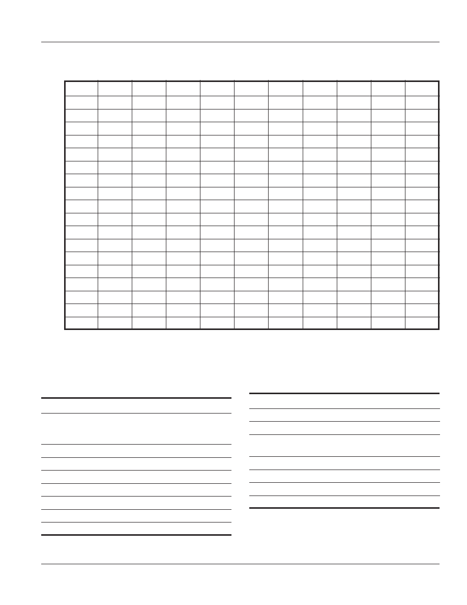
FAST ACCESS TIME
Symbol
Parameter
-250
-200
Units
t
KQ
Clock Access Time
2.6
3.2
ns
t
KC
Cycle Time
4
5
ns
Frequency
250
200
MHz
Integrated Silicon Solution, Inc. -- www.issi.com --
1-800-379-4774
3
ADVANCED INFORMATION Rev. 00A
07/17/02
IS61NVVP25672
IS61NVVP51236
ISSI
Æ
PIN DESCRIPTIONS
A
Synchronous Address Inputs
A0, A1
Synchronous Address Inputs. These
pins must tied to the two LSBs of the
address bus.
ADV
Synchronous Burst Address Advance
BW
a-
BW
h
Synchronous Byte Write Enable
CE
,
CE2
, CE2 Synchronous Chip Enable
CLK
Synchronous Clock
CKE
Clock Enable
DQa-DQh
Synchronous Data Input/Output
DQPa-DQPh
Parity Data Input/Output
GND
Ground
MODE
Burst Sequence Mode Selection
OE
Output Enable
TCK, TDI
JTAG Boundary Scan Pins
TDO, TMS
V
CC
+1.8V Power Supply
V
CCQ
Isolated Output Buffer Supply: 1.8V
WE
Write Enable
ZZ
Snooze Enable
PIN CONFIGURATION -- 256K X 72, 209-Ball PBGA (TOP VIEW)
1
2
3
4
5
6
7
8
9
10
11
A
DQg
DQg
A
CE2
A
ADV
A
CE2
A
DQb
DQb
B
DQg
DQg
BW
c
BW
g
NC
WE
A
BW
b
BW
f
DQb
DQb
C
DQg
DQg
BW
h
BW
d
NC
CE
NC
BW
e
BW
a
DQb
DQb
D
DQg
DQg
GND
NC
NC
OE
NC
NC
GND
DQb
DQb
E
DQPg
DQPc
V
CCQ
V
CCQ
V
CC
V
CC
V
CC
V
CCQ
V
CCQ
DQPf
DQPb
F
DQc
DQc
GND
GND
GND
NC
GND
GND
GND
DQf
DQf
G
DQc
DQc
V
CCQ
V
CCQ
V
CC
NC
V
CC
V
CCQ
V
CCQ
DQf
DQf
H
DQc
DQc
GND
GND
GND
NC
GND
GND
GND
DQf
DQf
J
DQc
DQc
V
CCQ
V
CCQ
V
CC
NC
V
CC
V
CCQ
V
CCQ
DQf
DQf
K
NC
NC
CLK
NC
GND
CKE
GND
NC
NC
NC
NC
L
DQh
DQh
V
CCQ
V
CCQ
VCC
NC
V
CC
V
CCQ
V
CCQ
DQa
DQa
M
DQh
DQh
GND
GND
GND
NC
GND
GND
GND
DQa
DQa
N
DQh
DQh
V
CCQ
V
CCQ
VCC
NC
V
CC
V
CCQ
V
CCQ
DQa
DQa
P
DQh
DQh
GND
GND
GND
ZZ
GND
GND
GND
DQa
DQa
R
DQPd
DQPh
V
CCQ
V
CCQ
V
CC
V
CC
V
CC
V
CCQ
V
CCQ
DQPa
DQPe
T
DQd
DQd
GND
NC
NC
MODE
NC
NC
GND
DQe
DQe
U
DQd
DQd
NC
A
NC
A
NC
A
NC
DQe
DQe
V
DQd
DQd
A
A
A
A1
A
A
A
DQe
DQe
W
DQd
DQd
TMS
TDI
A
A0
A
TDO
TCK
DQe
DQe
11 x 19 Ball BGA--14 x 22 mm
2
Body--1 mm Ball Pitch
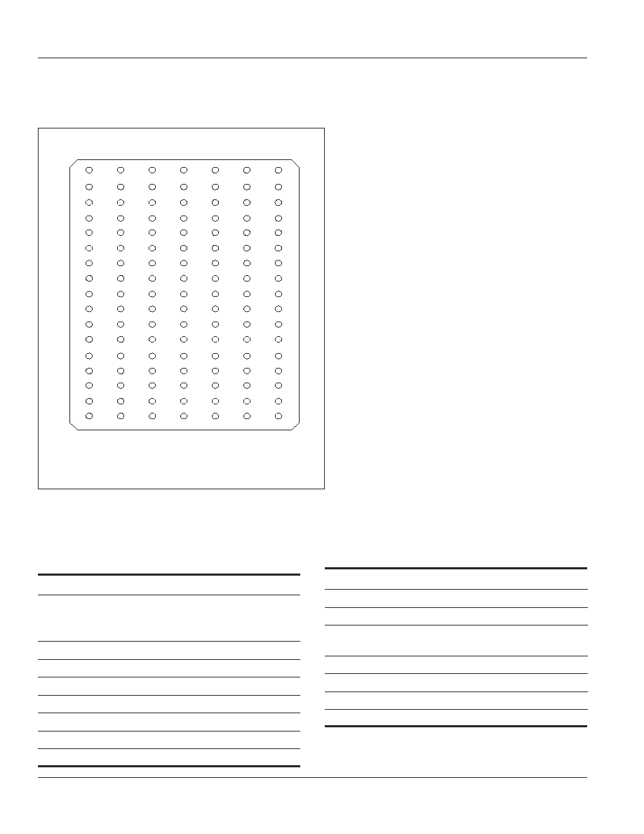
4
Integrated Silicon Solution, Inc. -- www.issi.com --
1-800-379-4774
ADVANCED INFORMATION Rev. 00A
07/17/02
IS61NVVP25672
IS61NVVP51236
ISSI
Æ
PIN CONFIGURATION
119-pin PBGA (Top View)
512K x 36
PIN DESCRIPTIONS
A
Synchronous Address Inputs
A0, A1
Synchronous Address Inputs. These
pins must tied to the two LSBs of the
address bus.
ADV
Synchronous Burst Address Advance
BW
a-
BW
h
Synchronous Byte Write Enable
CE
,
CE2
, CE2 Synchronous Chip Enable
CLK
Synchronous Clock
CKE
Clock Enable
DQa-DQd
Synchronous Data Input/Output
DQPa-DQPd
Parity Data Input/Output
GND
Ground
MODE
Burst Sequence Mode Selection
OE
Output Enable
TCK, TDI
JTAG Boundary Scan Pins
TDO, TMS
V
CC
1.8V Power Supply
V
CCQ
Isolated Output Buffer Supply: 1.8V
WE
Write Enable
ZZ
Snooze Enable
A
B
C
D
E
F
G
H
J
K
L
M
N
P
R
T
U
VCCQ
NC
NC
DQc
DQc
VCCQ
DQc
DQc
VCCQ
DQd
DQd
VCCQ
DQd
DQd
NC
NC
VCCQ
A
CE2
A
DQPc
DQc
DQc
DQc
DQc
VCC
DQd
DQd
DQd
DQd
DQPd
A
NC
TMS
A
A
A
GND
GND
GND
BW
c
GND
NC
GND
BW
d
GND
GND
GND
MODE
A
TDI
A
ADV
VCC
NC
CE
OE
A
WE
VCC
CLK
NC
CKE
A1
A0
VCC
A
TCK
A
A
A
GND
GND
GND
BW
b
GND
NC
GND
BW
a
GND
GND
GND
NC
A
TDO
A
CE2
A
DQPb
DQb
DQb
DQb
DQb
VCC
DQa
DQa
DQa
DQa
DQPa
A
NC
NC
VCCQ
NC
NC
DQb
DQb
VCCQ
DQb
DQb
VCCQ
DQa
DQa
VCCQ
DQa
DQa
NC
ZZ
VCCQ
1
2
3
4
5
6
7
Integrated Silicon Solution, Inc. -- www.issi.com --
1-800-379-4774
5
ADVANCED INFORMATION Rev. 00A
07/17/02
IS61NVVP25672
IS61NVVP51236
ISSI
Æ
SYNCHRONOUS TRUTH TABLE
(1)
Address
Operation
Used
CS
CS
CS
CS
CS
1
CS2
CS
CS
CS
CS
CS
2
ADV
WE
WE
WE
WE
WE
BW
BW
BW
BW
BW
x
OE
OE
OE
OE
OE
CKE
CKE
CKE
CKE
CKE
CLK
Not Selected Continue
N/A
X
X
X
H
X
X
X
L
Not Selected
N/A
H
X
X
L
X
X
X
L
Not Selected
N/A
X
L
X
L
X
X
X
L
Not Selected
N/A
X
X
H
L
X
X
X
L
Begin Burst Read
External Address
L
H
L
L
H
X
L
L
Continue Burst Read
Next Address
X
X
X
H
X
X
L
L
NOP/Dummy Read
External Address
L
H
L
L
H
X
H
L
Dummy Read
Next Address
X
X
X
H
X
X
H
L
Begin Burst Write
External Address
L
H
L
L
L
L
X
L
Continue Burst Write
Next Address
X
X
X
H
X
L
X
L
NOP/Write Abort
N/A
L
H
L
L
L
H
X
L
Write Abort
Next Address
X
X
X
H
X
H
X
L
Ignore Clock
Current Address
X
X
X
X
X
X
X
H
Notes:
1. "X" means don't care.
2. The rising edge of clock is symbolized by
3. A continue deselect cycle can only be entered if a deselect cycle is executed first.
4.
WE
= L means Write operation in Write Truth Table.
WE
= H means Read operation in Write Truth Table.
5. Operation finally depends on status of asynchronous pins (ZZ and
OE
).
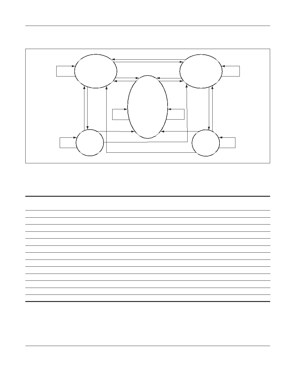
STATE DIAGRAM
BURST
READ
DESELECT
BURST
WRITE
BEGIN
READ
BEGIN
WRITE
READ
WRITE
READ
WRITE
BURST
BURST
BURST
DS
DS
DS
READ
DS
DS
READ
WRITE
WRITE
BURST
BURST
WRITE
READ