
Integrated Silicon Solution, Inc. -- 1-800-379-4774
1
Rev. B
06/29/06
ISSI
Æ
36 Mb (1M x 36 & 2M x 18)
QUAD (Burst of 2) Synchronous SRAMs
Features
∑ 1M x 36 or 2M x 18.
∑ On-chip delay-locked loop (DLL) for wide data
valid window.
∑ Separate read and write ports with concurrent
read and write operations.
∑ Synchronous pipeline read with early write oper-
ation.
∑ Double data rate (DDR) interface for read and
write input ports.
∑ Fixed 2-bit burst for read and write operations.
∑ Clock stop support.
∑ Two input clocks (K and K) for address and con-
trol registering at rising edges only.
∑ Two input clocks (C and C) for data output con-
trol.
∑ Two echo clocks (
CQ and CQ) that are delivered
simultaneously with data.
∑ +1.8V core power supply and 1.5, 1.8V V
DDQ
,
used with 0.75, 0.9V V
REF
.
∑ HSTL input and output levels.
∑ Registered addresses, write and read controls,
byte writes, data in, and data outputs.
∑ Full data coherency.
∑ Boundary scan using limited set of JTAG 1149.1
functions.
∑ Byte write capability.
∑ Fine ball grid array (FBGA) package
- 15mm x 17mm body size
- 1mm pitch
- 165-ball (11 x 15) array
∑ Programmable impedance output drivers via 5x
user-supplied precision resistor.
Description
The 36Mb
IS61QDB21Mx36 and
IS61QDB22Mx18 are synchronous, high-perfor-
mance CMOS static random access memory
(SRAM) devices. These SRAMs have separate I/Os,
eliminating the need for high-speed bus turnaround.
The rising edge of K clock initiates the read/write
operation, and all internal operations are self-timed.
Refer to the Timing Reference Diagram for Truth
Table on page
8 for a description of the basic opera-
tions of these SRAMs.
The input address bus operates at double data rate.
The following are registered internally on the rising
edge of the K clock:
∑ Read address
∑ Read enable
∑ Write enable
∑ Byte writes
∑ Data-in for early writes
The following are registered on the rising edge of
the K clock:
∑ Write address
∑ Byte writes
∑ Data-in for second burst addresses
Byte writes can change with the corresponding data-
in to enable or disable writes on a per-byte basis. An
internal write buffer enables the data-ins to be regis-
tered half a cycle earlier than the write address. The
first data-in burst is clocked at the same time as the
write command signal, and the second burst is timed
to the following rising edge of the K clock.
During the burst read operation, the data-outs from
the first burst are updated from output registers off
the second rising edge of the C clock (1.5 cycles
later). The data-outs from the second burst are
updated with the third rising edge of the C clock. The
K and K clocks are used to time the data-outs when-
ever the C and C clocks are tied high.
The device is operated with a single +1.8V power
supply and is compatible with HSTL I/O interfaces.
.
JULY 2006
2
Integrated Silicon Solution, Inc. -- 1-800-379-4774
Rev. B
06/29/06
ISSI
Æ
36 Mb (1M x 36 & 2M x 18)
QUAD (Burst of 2) Synchronous SRAMs
x36 FBGA Pinout
(Top View)
1
2
3
4
5
6
7
8
9
10
11
A
CQ
V
SS
/SA
NC/SA*
W
BW
2
K
BW
1
R
SA
V
SS
/SA
CQ
B
Q27
Q18
D18
SA
BW
3
K
BW
0
SA
D17
Q17
Q8
C
D27
Q28
D19
V
SS
SA
SA
SA
V
SS
D16
Q7
D8
D
D28
D20
Q19
V
SS
V
SS
V
SS
V
SS
V
SS
Q16
D15
D7
E
Q29
D29
Q20
V
DDQ
V
SS
V
SS
V
SS
V
DDQ
Q15
D6
Q6
F
Q30
Q21
D21
V
DDQ
V
DD
V
SS
V
DD
V
DDQ
D14
Q14
Q5
G
D30
D22
Q22
V
DDQ
V
DD
V
SS
V
DD
V
DDQ
Q13
D13
D5
H
Doff
V
REF
V
DDQ
V
DDQ
V
DD
V
SS
V
DD
V
DDQ
V
DDQ
V
REF
ZQ
J
D31
Q31
D23
V
DDQ
V
DD
V
SS
V
DD
V
DDQ
D12
Q4
D4
K
Q32
D32
Q23
V
DDQ
V
DD
V
SS
V
DD
V
DDQ
Q12
D3
Q3
L
Q33
Q24
D24
V
DDQ
V
SS
V
SS
V
SS
V
DDQ
D11
Q11
Q2
M
D33
Q34
D25
V
SS
V
SS
V
SS
V
SS
V
SS
D10
Q1
D2
N
D34
D26
Q25
V
SS
SA
SA
SA
V
SS
Q10
D9
D1
P
Q35
D35
Q26
SA
SA
C
SA
SA
Q9
D0
Q0
R
TDO
TCK
SA
SA
SA
C
SA
SA
SA
TMS
TDI
Note: The following pins are reserved for higher densities: A3 for 64Mb, 10A for 144Mb, and 2A for 288Mb.
x18 FBGA Pinout
(Top View)
1
2
3
4
5
6
7
8
9
10
11
A
CQ
V
SS
/SA*
SA
W
BW
1
K
NC
R
SA
V
SS
/SA*
CQ
B
NC
Q9
D9
SA
NC
K
BW
0
SA
NC
NC
Q8
C
NC
NC
D10
V
SS
SA
SA
SA
V
SS
NC
Q7
D8
D
NC
D11
Q10
V
SS
V
SS
V
SS
V
SS
V
SS
NC
NC
D7
E
NC
NC
Q11
V
DDQ
V
SS
V
SS
V
SS
V
DDQ
NC
D6
Q6
F
NC
Q12
D12
V
DDQ
V
DD
V
SS
V
DD
V
DDQ
NC
NC
Q5
G
NC
D13
Q13
V
DDQ
V
DD
V
SS
V
DD
V
DDQ
NC
NC
D5
H
Doff
V
REF
V
DDQ
V
DDQ
V
DD
V
SS
V
DD
V
DDQ
V
DDQ
V
REF
ZQ
J
NC
NC
D14
V
DDQ
V
DD
V
SS
V
DD
V
DDQ
NC
Q4
D4
K
NC
NC
Q14
V
DDQ
V
DD
V
SS
V
DD
V
DDQ
NC
D3
Q3
L
NC
Q15
D15
V
DDQ
V
SS
V
SS
V
SS
V
DDQ
NC
NC
Q2
M
NC
NC
D16
V
SS
V
SS
V
SS
V
SS
V
SS
NC
Q1
D2
N
NC
D17
Q16
V
SS
SA
SA
SA
V
SS
NC
NC
D1
P
NC
NC
Q17
SA
SA
C
SA
SA
NC
D0
Q0
R
TDO
TCK
SA
SA
SA
C
SA
SA
SA
TMS
TDI
Note: The following pins are reserved for higher densities: 10A for
72Mb and 2A for 144Mb.
Integrated Silicon Solution, Inc. -- 1-800-379-4774
3
Rev. B
06/29/06
ISSI
Æ
36 Mb (1M x 36 & 2M x 18)
QUAD (Burst of 2) Synchronous SRAMs
Pin Description
Symbol
Pin Number
Description
K, K
6B, 6A
Input clock.
C, C
6P, 6R
Input clock for output data control.
CQ, CQ
11A, 1A
Output echo clock.
Doff
1H
DLL disable when low.
SA
9A, 4B, 8B, 5C, 6C, 7C, 5N, 6N, 7N, 4P, 5P, 7P, 8P, 3R, 4R, 5R,
7R, 8R, 9R
1M x 36 address inputs.
SA
3A, 9A, 4B, 8B, 5C, 6C, 7C, 5N, 6N, 7N, 4P, 5P, 7P, 8P, 3R, 4R,
5R, 7R, 8R, 9R
2M x 18 address inputs.
D0≠D8
D9≠D17
D18≠D26
D27≠D35
10P, 11N, 11M, 10K, 11J, 11G, 10E, 11D, 11C
10N, 9M, 9L, 9J, 10G, 9F, 10D, 9C, 9B
3B, 3C, 2D, 3F, 2G, 3J, 3L, 3M, 2N
1C, 1D, 2E, 1G, 1J, 2K, 1M, 1N, 2P
1M x 36 data inputs.
Q0≠Q8
Q9≠Q17
Q18≠Q26
Q27≠Q35
11P, 10M, 11L, 11K, 10J, 11F, 11E, 10C, 11B
9P, 9N, 10L, 9K, 9G, 10F, 9E, 9D, 10B
2B, 3D, 3E, 2F, 3G, 3K, 2L, 3N, 3P
1B, 2C, 1E, 1F, 2J, 1K, 1L, 2M, 1P
1M x 36 data outputs.
D0≠D8
D9≠D17
10P, 11N, 11M, 10K, 11J, 11G, 10E, 11D, 11C
3B, 3C, 2D, 3F, 2G, 3J, 3L, 3M, 2N
2M x 18 data inputs.
Q0≠Q8
Q9≠Q17
11P, 10M, 11L, 11K, 10J, 11F, 11E, 10C, 11B
2B, 2D, 3E, 2F, 3G, 2K, 2L, 3N, 3P
2M x 18 data outputs.
W
4A
Write control, active low.
R
8A
Read control, active low.
BW
0,
BW
1,
BW
2,
BW
3
7B, 7A, 5A,5B
1M x 36 byte write control, active low.
BW
0,
BW
1
7B, 5A
2M x 18 byte write control, active low.
V
REF
2H, 10H
Input reference level.
V
DD
5F, 7F, 5G, 7G, 5H, 7H, 5J, 7J, 5K, 7K
Power supply.
V
DDQ
4E,8E,4F,8F,4G,8G,3H,4H,8H,9H,4J,8J,4K,8K,4L,8L
Output power supply.
V
SS
2A, 10A, 4C, 8C, 4D, 5D, 6D, 7D, 8D, 5E, 6E, 7E, 6F, 6G, 6H, 6J,
6K, 5L, 6L, 7L, 4M, 8M, 4N, 8N
Power supply.
ZQ
11H
Output driver impedance control.
TMS, TDI, TCK
10R, 11R, 2R
IEEE 1149.1 test inputs (1.8V LVTTL lev-
els).
TDO
1R
IEEE 1149.1 test output (1.8V LVTTL level).
4
Integrated Silicon Solution, Inc. -- 1-800-379-4774
Rev. B
06/29/06
ISSI
Æ
36 Mb (1M x 36 & 2M x 18)
QUAD (Burst of 2) Synchronous SRAMs
SRAM Features
Read Operations
The SRAM operates continuously in a burst-of-two mode. Read cycles are started by registering R in active
low state at the rising edge of the K clock. A second set of clocks, C and C, are used to control the timing to
the outputs. A set of free-running echo clocks, CQ and CQ, are produced internally with timings identical to
the data-outs. The echo clocks can be used as data capture clocks by the receiver device.
When the C and C clocks are connected high, the K and K clocks assume the function of those clocks. In this
case, the data corresponding to the first address is clocked 1.5 cycles later by the rising edge of the K clock.
The data corresponding to the second burst is clocked 2 cycles later by the following rising edge of the K
clock.
A NOP operation (R is high) does not terminate the previous read.
Write Operations
Write operations can also be initiated at every rising edge of the K clock whenever W is low. The write
address is provided 0.5 cycles later, registered by the rising edge of K. Again, the write always occurs in
bursts of two.
The write data is provided in an `early write' mode; that is, the data-in corresponding to the first address of the
burst, is presented 0.5 cycles earlier or at the rising edge of the preceding K clock. The data-in corresponding
to the second write burst address follows next, registered by the rising edge of K.
The data-in provided for writing is initially kept in write buffers. The information on these buffers is written into
the array on the following write cycle. A read cycle to the last write address produces data from the write
buffers. Similarly, a read address followed by the same write address produces the latest write data. The
SRAM maintains data coherency.
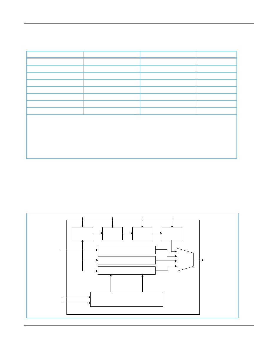
Block Diagram
1M x 36
(2M x 18)
Memory
Array
W
r
i
t
e/Read Dec
ode
S
ense Am
ps
Write Driver
Select Output Control
Data
Reg
Add
Reg
Control
Logic
Clock
Gen
O
u
tput Reg
O
u
t
p
u
t
Select
O
u
t
put Dr
i
v
er
72
(or 36)
72
(or 36)
36 (or 18)
Q (Data-Out)
CQ, CQ
(Echo Clock Out)
D (Data-In)
36 (or 18)
Address
R
W
BW
x
K
K
C
C
4 (or 2)
19 (or 20)
19 (or 20)
36 (or 18)
36 (or 18)

Integrated Silicon Solution, Inc. -- 1-800-379-4774
5
Rev. B
06/29/06
ISSI
Æ
36 Mb (1M x 36 & 2M x 18)
QUAD (Burst of 2) Synchronous SRAMs
During a write, the byte writes independently control which byte of any of the two burst addresses is written
(see X18/X36 Write Truth Tables on page
9 and Timing Reference Diagram for Truth Table on page 8).
Whenever a write is disabled (W is high at the rising edge of K), data is not written into the memory.
RQ Programmable Impedance
An external resistor, RQ, must be connected between the ZQ pin on the SRAM and V
SS
to enable the SRAM
to adjust its output driver impedance. The value of RQ must be 5x the value of the intended line impedance
driven by the SRAM. For example, an RQ of 250
results in a driver impedance of 50. The allowable range
of RQ to guarantee impedance matching is between 175
and 350, with the tolerance described in
Programmable Impedance Output Driver DC Electrical Characteristics on page 14. The RQ resistor should
be placed less than two inches away from the ZQ ball on the SRAM module. The capacitance of the loaded
ZQ trace must be less than 3 pF.
The ZQ pin can also be directly connected to V
DDQ
to obtain a minimum impedance setting. ZQ must never
be connected to V
SS
.
Programmable Impedance and Power-Up Requirements
Periodic readjustment of the output driver impedance is necessary as the impedance is greatly affected by
drifts in supply voltage and temperature. At power-up, the driver impedance is in the middle of allowable
impedances values. The final impedance value is achieved within 1024 clock cycles.
Clock Consideration
This device uses an internal DLL for maximum output data valid window. It can be placed in a stopped-clock
mode to minimize power and requires only 1024 cycles to restart.
No clocks can be issued until V
DD
reaches its allowable operating range.
Single Clock Mode
This device can be also operated in single-clock mode. In this case, C and C are both connected high at
power-up and must never change. Under this condition, K and K will control the output timings.
Either clock pair must have both polarities switching and must never connect to V
REF
, as they are not differ-
ential clocks
Depth Expansion
Separate input and output ports enable easy depth expansion, as each port can be selected and deselected
independently. Read and write operations can occur simultaneously without affecting each other. Also, all
pending read and write transactions are always completed prior to deselecting the corresponding port.
In the following application example, the second pair of C and C clocks is delayed such that the return data
meets the data setup and hold times at the bus master.
6
Integrated Silicon Solution, Inc. -- 1-800-379-4774
Rev. B
06/29/06
ISSI
Æ
36 Mb (1M x 36 & 2M x 18)
QUAD (Burst of 2) Synchronous SRAMs
Power-Up and Power-Down Sequences
The power supplies must be powered up in the following order:
1. V
DD
2. V
DDQ
3. V
REF
4. Inputs
The power-down sequence must be the reverse. V
DDQ
can be allowed to exceed V
DD
by no more than 0.6V.
Application Example
2M x 18
SA
R W BW
0
BW
1
C C K K
D
0≠17
Q
0≠17
ZQ
SRAM #4
R=250
Vt
Data-In 0≠71
Data-Out 0≠71
Address 0≠79
R
W
BW
0≠7
Memory
Controller
Return CLK
Source CLK
Return CLK
Source CLK
SA
R W BW
0
BW
1
C C K K
D
0≠17
Q
0≠17
ZQ
SRAM #1
R=250
Vt
Vt
R
Vt
Vt
R=50
Vt=V
REF
R
Integrated Silicon Solution, Inc. -- 1-800-379-4774
7
Rev. B
06/29/06
ISSI
Æ
36 Mb (1M x 36 & 2M x 18)
QUAD (Burst of 2) Synchronous SRAMs
The Timing Reference Diagram for Truth Table on page
8 is helpful in understanding the clock and write truth
tables, as it shows the cycle relationship between clocks, address, data in, data out, and controls. All read
and write commands are issued at the beginning of cycle "t".
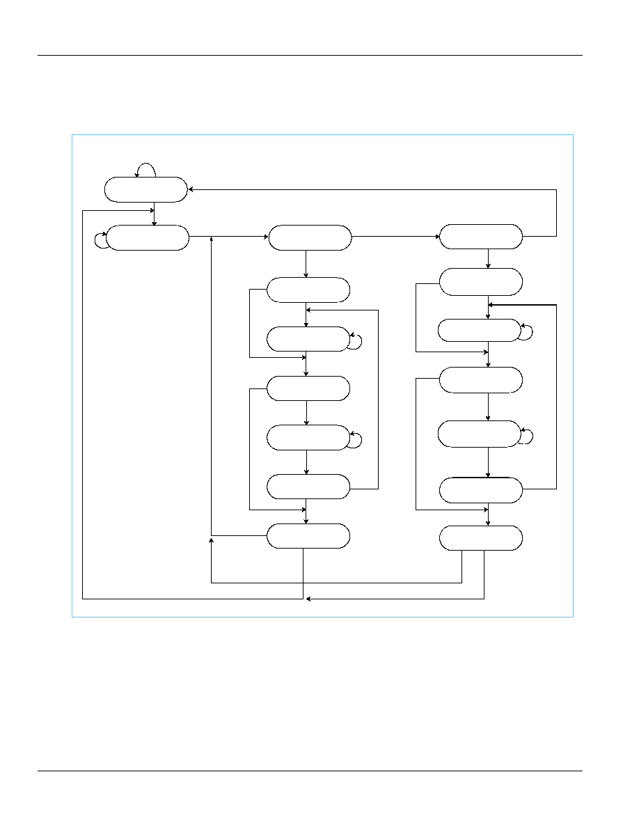
State Diagram
Power Up
Write NOP
Load New
Write Address
DDR Write
Read NOP
Load New
Read Address
DDR Read
Read
Write
Read
Write
Read
Write
Read
Write
Always
(fixed)
Always
(fixed)
Notes: 1. Internal burst counter is fixed as two-bit linear; that is, when first address is A0+0, next internal burst address is A0+1.
2. Read refers to read active status with R = low. Read refers to read inactive status with R = high.
5. State machine control timing sequence is controlled by K.
4. The read and write state machines can be active simultaneously.
3. Write refers to write active status with W = low. Write refers to write inactive status with W = high.
8
Integrated Silicon Solution, Inc. -- 1-800-379-4774
Rev. B
06/29/06
ISSI
Æ
36 Mb (1M x 36 & 2M x 18)
QUAD (Burst of 2) Synchronous SRAMs
Timing Reference Diagram for Truth Table
Clock Truth Table
(Use the following table with the Timing Reference Diagram for Truth Table.)
Mode
Clock
Controls
Data-In
Data-Out
K
R
W
D
B
D
B+1
Q
A
Q
A+1
Stop Clock
Stop
X
X
Previous state
Previous State
Previous state
Previous state
No Operation (NOP)
L
H
H
H
X
X
High-Z
High-Z
Read A
L
H
L
X
X
X
D out at C
(t + 1.5)
D out at C (t + 2)
Write B
L
H
X
L
D in at K (t)
D in at K
(t + 0.5)
X
X
Notes:
1. The internal burst counter is always fixed as two-bit.
2. X = don't care; H = logic "1"; L = logic "0".
3. A read operation is started when control signal R is active low
4. A write operation is started when control signal W is active low. Before entering into the stop clock, all pending read and write
commands must be completed.
5. For timing definitions, refer to the AC Characteristics on page 16. Signals must have AC specifications at timings indicated in
parenthesis with respect to switching clocks K, K, C, and C.
t
t+1
t+2
t+3
Read A
Write B
Read C
Write D
A
B
C
D
Q
A
Q
A+1
Q
C+2
Q
C+3
K Clock
K Clock
W
R
BW
0,1,2,3
Address
Data-In
Data-Out
C Clock
C Clock
CQ Clock
CQ Clock
Cycle
D
B
D
B+1
D
D
D
D+1
Integrated Silicon Solution, Inc. -- 1-800-379-4774
9
Rev. B
06/29/06
ISSI
Æ
36 Mb (1M x 36 & 2M x 18)
QUAD (Burst of 2) Synchronous SRAMs
X36 Write Truth Table
Use the following table with the Timing Reference Diagram for Truth Table on
page
8.
Operation
K(t)
K
(t + 0.5)
BW
0
BW
1
BW
2
BW
3
D
B
D
B+1
Write Byte 0
L
H
L
H
H
H
D0-8 (t)
Write Byte 1
L
H
H
L
H
H
D9-17 (t)
Write Byte 2
L
H
H
H
L
H
D18-26 (t)
Write Byte 3
L
H
H
H
H
L
D27-35 (t)
Write All Bytes
L
H
L
L
L
L
D0-35 (t)
Abort Write
L
H
H
H
H
H
Don't care
Write Byte 0
L
H
L
H
H
H
D0-8 (t + 0.5)
Write Byte 1
L
H
H
L
H
H
D9-17 (t + 0.5)
Write Byte 2
L
H
H
H
L
H
D18-26 (t + 0.5)
Write Byte 3
L
H
H
H
H
L
D27-35 (t + 0.5)
Write All Bytes
L
H
L
L
L
L
D0-35 (t + 0.5)
Abort Write
L
H
H
H
H
H
Don't care
Notes;
1. For all cases. W must be active low during the rising edge of K occurring at time t.
2. For timing definitions, refer to the AC Characteristics on page 16. Signals must have AC specifications with respect to switching
clocks K and K.
X18 Write Truth Table
(Use this table with the Timing Reference Diagram for Truth Table on page
8.)
Operation
K(t)
K
(t + 0.5)
BW
0
BW
1
D
B
D
B+1
Write Byte 0 on B
L
H
L
H
D0≠8 (t)
Write Byte 1 on B
L
H
H
L
D9≠17 (t)
Write All Bytes on B
L
H
L
L
D0≠17 (t)
Abort Write on B
L
H
H
H
Don't care
Write Byte 1 on B+1
L
H
L
H
D0≠8(t + 0.5)
Write Byte 2 on B+1
L
H
H
L
D9≠17(t + 0.5)
Write All Bytes on B+1
L
H
L
L
D0≠17(t + 0.5)
Abort Write on B+1
L
H
H
H
Don't care
Notes;
1. Refer to Timing Reference Diagram for Truth Table on page
8. Cycle time starts at n and is referenced to the K clock.
2. For all cases, W must be active low during the rising edge of K occurring at t.
3. For timing definitions, refer to the AC Characteristics on page 16. Signals must have AC specs with respect to switching clocks K
and K.
10
Integrated Silicon Solution, Inc. -- 1-800-379-4774
Rev. B
06/29/06
ISSI
Æ
36 Mb (1M x 36 & 2M x 18)
QUAD (Burst of 2) Synchronous SRAMs
Absolute Maximum Ratings
Item
Symbol
Rating
Units
Power supply voltage
V
DD
-0.5 to 2.6
V
Output power supply voltage
V
DDQ
-0.5 to 2.6
V
Input voltage
V
IN
-0.5 to 2.6
V
Data out voltage
V
DOUT
-0.5 to 2.6
V
Operating temperature
T
A
0 to 70
∞ C
Junction temperature
T
J
110
∞ C
Storage temperature
T
STG
-55 to +125
∞ C
Note: Stresses greater than those listed in this table can cause permanent damage to the device. This is a stress rating only and func-
tional operation of the device at these or any other conditions above those indicated in the operational sections of this datasheet is not
implied. Exposure to absolute maximum rating conditions for extended periods may affect reliability.
Integrated Silicon Solution, Inc. -- 1-800-379-4774
11
Rev. B
06/29/06
ISSI
Æ
36 Mb (1M x 36 & 2M x 18)
QUAD (Burst of 2) Synchronous SRAMs
Recommended DC Operating Conditions
(T
A
= 0 to +
70∞ C)
Parameter
Symbol
Minimum
Typical
Maximum
Units
Notes
Supply voltage
V
DD
1.8 - 5%
1.8 + 5%
V
1
Output driver supply voltage
V
DDQ
1.4
1.9
V
1
Input high voltage
V
IH
V
REF
+0.1
V
DDQ
+ 0.2
V
1, 2
Input low voltage
V
IL
-0.2
V
REF
- 0.1
V
1, 3
Input reference voltage
V
REF
0.68
0.95
V
1, 5
Clocks signal voltage
V
IN - CLK
-0.2
V
DDQ
+ 0.2
V
1, 4
1. All voltages are referenced to V
SS
. All V
DD
, V
DDQ
, and V
SS
pins must be connected.
2. V
IH
(Max) AC = See 0vershoot and Undershoot Timings.
3. V
IL
(Min) AC = See 0vershoot and Undershoot Timings.
4. V
IN-CLK
specifies the maximum allowable DC excursions of each clock (K, K, C, and C).
5. Peak-to-peak AC component superimposed on V
REF
may not exceed 5% of V
REF.
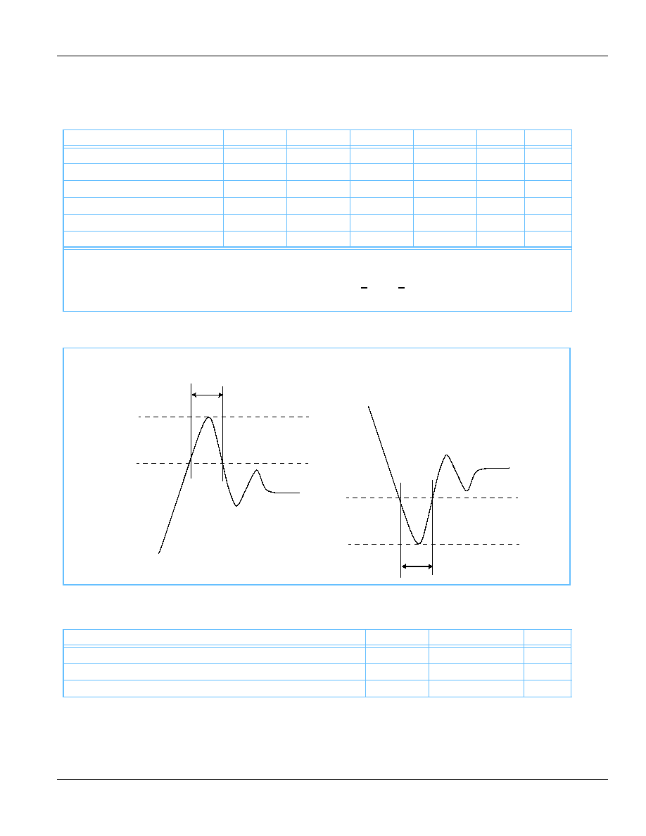
0vershoot and Undershoot Timings
PBGA Thermal Characteristics
Item
Symbol
Rating
Units
Thermal resistance junction to ambient (airflow = 1m/s)
R
JA
TBD
∞ C/W
Thermal resistance junction to case
R
JC
TBD
∞ C/W
Thermal resistance junction to pins
R
JB
TBD
∞ C/W
V
DDQ
20% Min Cycle Time
V
DDQ
+0.6V
GND-0.6V
GND
20% Min Cycle Time
Overshoot Timing
Undershoot Timing
V
IH
(Max) AC
V
IL
(Min) AC
12
Integrated Silicon Solution, Inc. -- 1-800-379-4774
Rev. B
06/29/06
ISSI
Æ
36 Mb (1M x 36 & 2M x 18)
QUAD (Burst of 2) Synchronous SRAMs
Capacitance
(T
A
= 0 to +
70∞ C, V
DD
= 1.8V -5%, +5%, f = 1MHz)
Parameter
Symbol
Test Condition
Maximum
Units
Input capacitance
C
IN
V
IN
= 0V
4
pF
Data-in capacitance (D0≠D35)
C
DIN
V
DIN
= 0V
4
pF
Data-out capacitance (Q0≠Q35)
C
OUT
V
OUT
= 0V
4
pF
Clocks Capacitance (K, K, C, C
DC Electrical Characteristics
(T
A
= 0 to + 70C, V
DD
= 1.8V -5%, +5%)
Parameter
Symbol
Minimum
Maximum
Units
Notes
x36 average power supply operating current
(I
OUT
= 0, V
IN
= V
IH
or V
IL
)
I
DD30
I
DD40
I
DD50
--
--
mA
1, 3
x18 average power supply operating current
(I
OUT
= 0, V
IN
= V
IH
or V
IL
)
I
DD30
I
DD40
I
DD50
--
--
1, 3
Power supply standby current
(R = V
IH
, W = V
IH
. All other inputs = V
IH
or V
IH
, I
IH
= 0)
I
SBSS
--
200
mA
1
Input leakage current, any input (except JTAG)
(V
IN
= V
SS
or V
DD
) I
LI
-2 +2 uA
Output leakage current
(V
OUT
= V
SS
or V
DDQ
, Q in High-Z) I
LO
-5 +5 uA
Output "high" level voltage (I
OH
= -6mA) V
OH
V
DDQ
-0.4 V
DDQ
Output "low" level voltage (I
OL
= +6mA) V
OL
V
SS
V
SS
+0.4 V 2, 4
JTAG leakage current
(V
IN
= V
SS
or V
DD
) I
LIJTAG
-100 uA
5
1. I
OUT
= chip output current.
2. Minimum impedance output driver.
3. The numeric suffix indicates the part operating at speed, as indicated in AC Characteristics on page 16 (that is, I
DD25
indicates
2.5ns cycle time).
4. JEDEC Standard JESD8-6 Class 1 compatible.
5. For JTAG inputs only.
6. Currents are estimates only and need to be verified.
800
700
600
800
700
600
mA
+100
V
2, 4
Integrated Silicon Solution, Inc. -- 1-800-379-4774
13
Rev. B
06/29/06
ISSI
Æ
36 Mb (1M x 36 & 2M x 18)
QUAD (Burst of 2) Synchronous SRAMs
Typical AC Input Characteristics
Item
Symbol
Minimum
Maximum
Notes
AC input logic high
V
IH
(ac)
V
REF
+ 0.4
1, 2, 3, 4
AC input logic low
V
IL
(ac)
V
REF
- 0.4
1, 2, 3, 4
Clock input logic high (K, K, C, C)
V
IH-CLK
(ac)
V
REF
+ 0.4
1, 2, 3
Clock input logic low (K, K, C, C)
V
IL-CLK
(ac)
V
REF
- 0.4
1, 2, 3
1. The peak-to-peak AC component superimposed on V
REF
may not exceed 5% of the DC component of V
REF
.
2. Performance is a function of V
IH
and V
IL
levels to clock inputs.
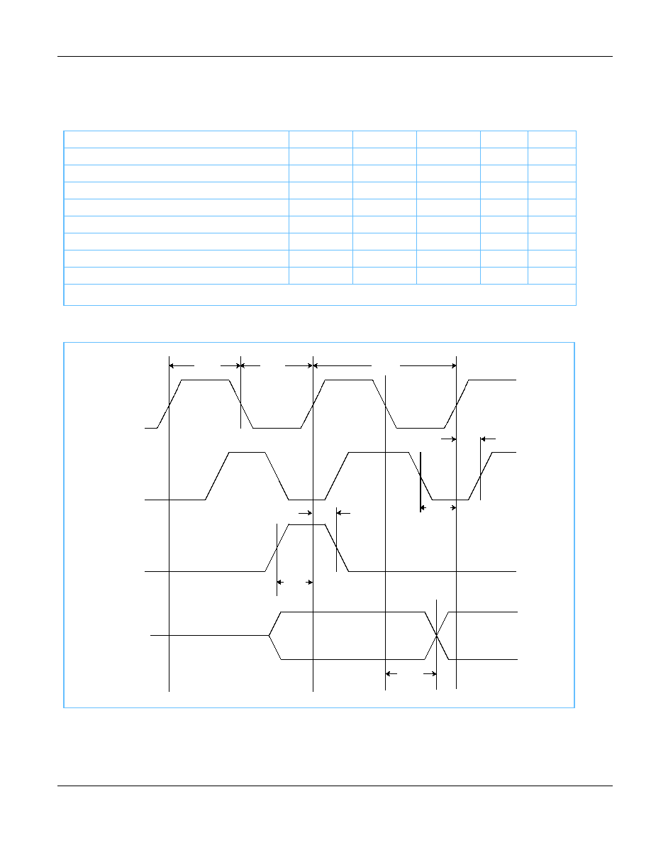
3. See the AC Input Definition diagram.
4. See the AC Input Definition diagram. The signals should swing monotonically with no steps rail-to-rail with input signals never ring-
ing back past VIH (AC) and VIL (AC) during the input setup and input hold window. VIH (AC) and VIL (AC) are used for timing pur-
poses only.
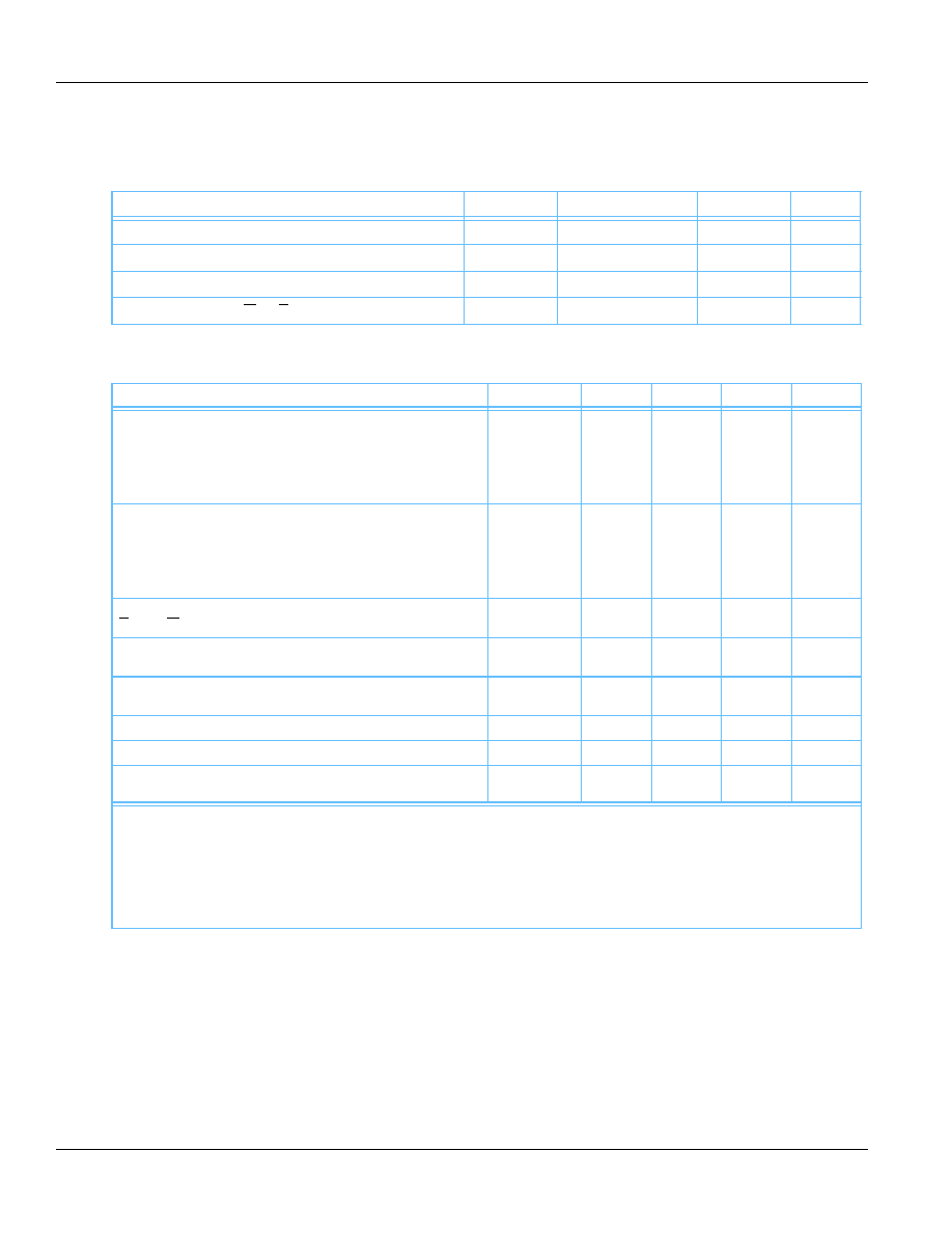
AC Input Definition
Programmable Impedance Output Driver DC Electrical Characteristics
(T
A
= 0 to +70
∞ C, V
DD
= 1.8V -5%, +5%, V
DDQ
= 1.5, 1.8V)
Parameter
Symbol
Minimum
Maximum
Units
Notes
Output "high" level voltage
V
OH
V
DDQ
/ 2
V
DDQ
V
1, 3
Output "low" level voltage
V
OL
V
SS
V
DDQ
/ 2
V
2, 3
1. I
OH
=
± 15% @ V
OH
= V
DDQ
/ 2 For: 175
RQ 350.
2. I
OL
=
± 15% @ V
OL
= V
DDQ
/ 2 For: 175
RQ 350.
3. Parameter tested with RQ = 250
and V
DDQ
= 1.5V.
V
IH
(AC)
V
REF
V
IL
(AC)
Setup
Time
Hold
Time
V
REF
K
K
V
RAIL
V
-RAIL
VDDQ
2
------------------
RQ
5
--------
/
VDDQ
2
------------------
RQ
5
--------
/
14
Integrated Silicon Solution, Inc. -- 1-800-379-4774
Rev. B
06/29/06
ISSI
Æ
36 Mb (1M x 36 & 2M x 18)
QUAD (Burst of 2) Synchronous SRAMs
AC Test Loading
Q
50
50
5pF
0.75, 0.9V
0.75, 0.9V
Test
Comparator
AC Test Conditions
(T
A
= 0 to +
70C, V
DD
= 1.8V -5%, +5%, V
DDQ
= 1.5, 1.8V)
Parameter
Symbol
Conditions
Units
Notes
Output driver supply voltage
V
DDQ
1.5, 1.8
V
Input high level
V
IH
1.25
0.25
V
Input Low Level
V
IL
V
Input reference voltage
V
REF
0.75
V
Input rise time
T
R
0.35
ns
Input fall time
T
F
0.35
ns
Output timing reference level
V
DDQ/2
V
Output load conditions
1, 2
1. See AC Test Loading.
2. Parameter tested with RQ = 250 and V
DDQ
= 1.5V.
Integrated Silicon Solution, Inc. -- 1-800-379-4774
15
Rev. B
06/29/06
ISSI
Æ
36 Mb (1M x 36 & 2M x 18)
QUAD (Burst of 2) Synchronous SRAMs
AC Characteristics
(T
A
= 0 to +
70C, V
DD
= 1.8V -5%, +5%)
Parameter
Symbol
30
(333MHz)
Units
Notes
Min
Max
Clock
Cycle time (K, K, C, C)
t
KHKH
3.0
4.0
ns
ns
ns
ns
ns
ns
ns
ns
ns
ns
ns
ns
ns
ns
Clock phase jitter (K, K, C, C)
t
KC-VAR
Clock high pulse (K, K, C, C)
t
KHKL
Clock low pulse (K, K, C, C)
t
KLKH
Clock to clock (K
H
>K
H
, C
H
>C
H
)
t
KHKH
Clock to data clock (K
H
>C
H
, K
H
>C
H
)
t
KHCH
DLL lock (K, C)
t
KC-
lock
K static to DLL reset
t
KC-
reset
Output Times
C, C high to output valid
t
CHQV
0.40
1, 3
1, 3
C, C high to output hold
t
CHQX
-0.40
C, C high to echo clock valid
t
CHCQV
0.35
3
C, C high to echo clock hold
t
CHCQX
-0.35
3
CQ, CQ high to output valid
t
CQHQV
0.25
1, 3
1, 3
1, 3
1, 3
CQ, CQ high to output hold
t
CQHQX
-0.25
C high to output high-Z
t
CHQZ
0.33
C high to output low-Z
t
CHQX1
-0.33
Setup Times
Address valid to K, K rising edge
t
AVKH
0.33
--
ns
2
Control inputs valid to K rising edge
t
IVKH
0.33
--
ns
2
Data-in valid to K, K rising edge
t
DVKH
0.33
--
ns
2
Hold Times
K rising edge to address hold
t
KHAX
0.33
--
ns
2
K rising edge to control inputs hold
t
KHIX
0.33
--
ns
2
K, K rising edge to data-in hold
t
KHDX
0.33
--
ns
2
1. See AC Test Loading on page 15.
2. During normal operation, V
IH
, V
IL
, T
RISE
, and T
FALL
of inputs must be within 20% of V
IH
, V
IL
, T
RISE
, and T
FALL
of clock.
3. If C, C are tied high, then K,
K
become the references for C,
C
timing parameters.
0.12
1.2
1.2
1.35
0.0
1.35
1024
30
cycle
cycle
16
Integrated Silicon Solution, Inc. -- 1-800-379-4774
Rev. B
06/29/06
ISSI
Æ
36 Mb (1M x 36 & 2M x 18)
QUAD (Burst of 2) Synchronous SRAMs
AC Characteristics
(T
A
= 0 to + 70C, V
DD
= 1.8V -5%, +5%)
Parameter
Symbol
40
(250MHz)
50
(200MHz)
Units
Notes
Min
Max
Min
Max
Clock
Cycle time (K, K, C, C)
t
KHKH
4.0
6.0
5.0
7.5
ns
Clock phase jitter (K, K, C, C)
t
KC-VAR
0.2
0.2
ns
Clock high pulse (K, K, C, C)
t
KHKL
1.6
2.0
ns
Clock low pulse (K, K, C, C)
t
KLKH
1.6
2.0
ns
Clock to clock (K
H
>K
H
, C
H
>C
H
)
t
KHKH
1.8
2.2
Clock to data clock (K
H
>C
H
, K
H
>C
H
)
t
KHCH
0.0
1.8
0.0
2.3
DLL lock (K, C)
t
KC-
lock
1024
1024
cycle
cycle
K static to DLL reset
t
KC-
reset
30
30
Output Times
C, C high to output valid
t
CHQV
0.45
0.45
ns
1, 3
C, C high to output hold
t
CHQX
-0.45
-0.45
ns
ns
1, 3
C, C high to echo clock valid
t
CHCQV
0.40
0.4
3
C, C high to echo clock hold
t
CHCQX
-0.40
-0.40
ns
3
CQ, CQ High to output valid
t
CQHQV
0.30
0.40
ns
1, 3
CQ, CQ high to output hold
t
CQHQX
-0.30
-0.40
ns
1, 3
C High to output high-Z
t
CHQZ
0.35
0.38
ns
1, 3
C High to output low-Z
t
CHQX1
-0.35
-0.38
ns
1, 3
Setup Times
Address valid to K, K rising edge
t
AVKH
0.35
--
0.4
--
ns
2
ns
2
ns
2
Control inputs valid to K rising edge
t
IVKH
0.35
--
0.4
--
Data-in valid to K, K rising edge
t
DVKH
0.35
--
0.4
--
Hold Times
K rising edge to address hold
t
KHAX
0.35
--
0.4
--
ns
2
ns
2
ns
2
K rising edge to Control Inputs Hold
t
KHIX
0.35
--
0.4
--
K, K rising edge to data-in hold
t
KHDX
0.35
--
0.4
--
1. See AC Test Loading on page 15.
2. During normal operation, V
IH
, V
IL
, T
RISE
, and T
FALL
of inputs must be within 20% of V
IH
, V
IL
, T
RISE
, and T
FALL
of clock.
3. If C, C are tied high, then K,
K
become the references for C,
C
timing parameters.
ns
ns
Integrated Silicon Solution, Inc. -- 1-800-379-4774
17
Rev. B
06/29/06
ISSI
Æ
36 Mb (1M x 36 & 2M x 18)
QUAD (Burst of 2) Synchronous SRAMs
Read and Deselect Cycles Timing Diagram
t
CHCQX
t
CHCQV
t
CHCQX
t
CHCQV
t
CQHQX
t
CQHQV
t
CHQV
t
CHQZ
t
CHQX
t
CHQV
t
CHQX
t
KLKH
t
KHKH
t
KHKL
t
KHIX
t
IVKH
t
KHAX
t
AVKH
t
KHKH
t
KLKH
t
KHKH
t
KHKL
Read
Read
NOP
Read
NOP
A1
A2
A3
Q1-1
Q1-2
Q2-1
Q2-2
Q3-1
K
K
SA
R
Q (Data Out)
C
C
CQ
CQ
t
KLKH
Notes: 1. Q1-1 refers to output from address A1+0, Q1-2 refers to output from address A1+1 (that is, the next internal
burst address following A1+0).
2. Outputs are disabled one cycle after an NOP.
Don't Care
Undefined
18
Integrated Silicon Solution, Inc. -- 1-800-379-4774
Rev. B
06/29/06
ISSI
Æ
36 Mb (1M x 36 & 2M x 18)
QUAD (Burst of 2) Synchronous SRAMs
Write and NOP Timing Diagram
t
KHDX
t
DVKH
t
KHIX
t
KHIX
t
IVKH
t
KHAX
t
AVKH
t
KHKH
t
KHKH
t
KLKH
t
KHKL
Write
Write
NOP
Write
NOP
A1
A2
A3
D1-1
D1-2
D2-1
D2-2
D3-1
D3-2
K
K
SA
W
D(Data In)
Don't Care
Undefined
Notes: 1. D1-1 refers to input to address A1+0, D1-2 refers to input to address A1+1 (that is, the next internal
burst address following A1+0).
2. BWx assumed active.
t
KHIX
t
IVKH
BW
Integrated Silicon Solution, Inc. -- 1-800-379-4774
19
Rev. B
06/29/06
ISSI
Æ
36 Mb (1M x 36 & 2M x 18)
QUAD (Burst of 2) Synchronous SRAMs
Read, Write, and NOP Timing Diagram
Read
Write
Read
Write
Read
Write
NOP
Write
NOP
A1
A2
A3
A4
A5
A6
A7
D2-1
D2-2
D4-1
D6-1
D6-2
D7-1
D7-2
D4-2
Q1-1
Q1-2
Q3-1
Q3-2
Q5-1
Q5-2
Notes: 1. If address A1=A2, data Q1-1=D2-1, data Q1-2=D2-2.
Write data is forwarded immediately as read results.
K
K
SA
W
R
D(Data In)
Q(Data Out)
C
C
CQ
CQ
Don't Care
Undefined
BWx
20
Integrated Silicon Solution, Inc. -- 1-800-379-4774
Rev. B
06/29/06
ISSI
Æ
36 Mb (1M x 36 & 2M x 18)
QUAD (Burst of 2) Synchronous SRAMs
IEEE 1149.1 TAP and Boundary Scan
The SRAM provides a limited set of JTAG functions to test the interconnection between SRAM I/Os and
printed circuit board traces or other components. There is no multiplexer in the path from I/O pins to the RAM
core.
In conformance with IEEE Standard 1149.1, the SRAM contains a TAP controller, instruction register,
boundary scan register, bypass register, and ID register.
The TAP controller has a standard 16-state machine that resets internally on power-up. Therefore, a TRST
signal is not required.
Signal List
∑ TCK: test clock
∑ TMS: test mode select
∑ TDI: test data-in
∑ TDO: test data-out
JTAG DC Operating Characteristics
(T
A
= 0 to +
70∞ C)
Operates with JEDEC Standard 8-5 (1.8V) logic signal levels
Parameter
Symbol
Minimum
Typical
Maximum
Units
Notes
JTAG input high voltage
V
IH1
1.3
--
V
DD
+0.3
V
1
JTAG input low voltage
V
IL1
-0.3
--
0.5
V
1
JTAG output high level
V
OH1
V
DD
-0.4
--
V
DD
V
1, 2
JTAG output low level
V
OL1
V
SS
--
0.4
V
1, 3
1. All JTAG inputs and outputs are LVTTL-compatible.
2. I
OH1
-|2mA|
3. I
OL1
+|2mA|.
JTAG AC Test Conditions
(T
A
= 0 to +
70∞ C, V
DD
= 1.8V -5%, +5%)
Parameter
Symbol
Conditions
Units
Input pulse high level
V
IH1
1.3
V
Input pulse low level
V
IL1
0.5
V
Input rise time
T
R1
1.0
ns
Input fall time
T
F1
1.0
ns
Input and output timing reference level
0.9
V
Integrated Silicon Solution, Inc. -- 1-800-379-4774
21
Rev. B
06/29/06
ISSI
Æ
36 Mb (1M x 36 & 2M x 18)
QUAD (Burst of 2) Synchronous SRAMs
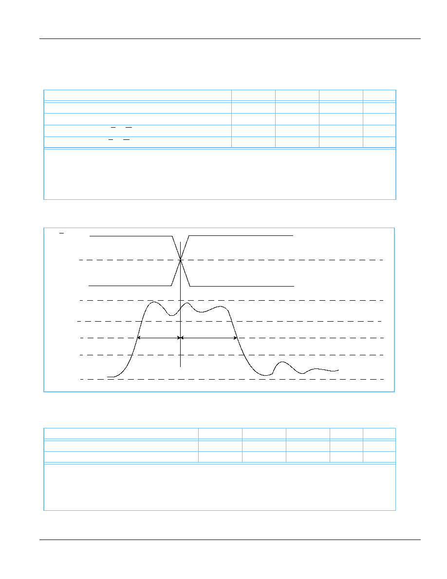
JTAG AC Characteristics
(T
A
= 0 to +
70∞ C, V
DD
= 1.8V -5%, +5%)
Parameter
Symbol
Minimum
Maximum
Units
Notes
TCK cycle time
t
THTH
20
--
ns
TCK high pulse width
t
THTL
7
--
ns
TCk low pulse width
t
TLTH
7
--
ns
TMS setup
t
MVTH
4
--
ns
TMS hold
t
THMX
4
--
ns
TDI setup
t
DVTH
4
--
ns
TDI hold
t
THDX
4
--
ns
TCK low to valid data
t
TLOV
--
7
ns
1
1. See AC Test Loading on page 15.
JTAG Timing Diagram
TCK
TMS
TDI
TDO
t
THTL
t
TLTH
t
THTH
t
THMX
t
THDX
t
TLOV
t
MVTH
t
DVTH
22
Integrated Silicon Solution, Inc. -- 1-800-379-4774
Rev. B
06/29/06
ISSI
Æ
36 Mb (1M x 36 & 2M x 18)
QUAD (Burst of 2) Synchronous SRAMs
Scan Register Definition
Register Name
Bit Size x18 or x36
Instruction
3
Bypass
1
ID
32
Boundary Scan
109
ID Register Definition
Part
Field Bit Number and Description
Revision Number
(31:29)
Part Configuration
(28:12)
JEDEC Code
(11:1)
Start Bit
(0)
2M x 18
000
00def0wx0t0q0b0s0
000 101 001 00
1
1M x 36
000
00def0wx0t0q0b0s0
000 101 001 00
1
Part Configuration Definition:
def = 010 for 36Mb
wx = 11 for x36, 10 for x18
t = 1 for DLL, 0 for non-DLL
q = 1 for Q
DB2, 0 for DDR
b = 1 for burst of 4, 0 for burst of 2
s = 1 for separate I/0, 0 for common I/O
Integrated Silicon Solution, Inc. -- 1-800-379-4774
23
Rev. B
06/29/06
ISSI
Æ
36 Mb (1M x 36 & 2M x 18)
QUAD (Burst of 2) Synchronous SRAMs
List of IEEE 1149.1 Standard Violations
∑ 7.2.1.b, e
∑ 7.7.1.a-f
∑ 10.1.1.b, e
∑ 10.7.1.a-d
∑ 6.1.1.d
Instruction Set
Code
Instruction
TDO Output
Notes
000
EXTEST
Boundary Scan Register
2,6
001
IDCODE
32-bit Identification Register
010
SAMPLE-Z
Boundary Scan Register
1, 2
011
PRIVATE
Do not use
5
100
SAMPLE
Boundary Scan Register
4
101
PRIVATE
Do not use
5
110
PRIVATE
Do not use
5
111
BYPASS
Bypass Register
3
1. Places Qs in high-Z in order to sample all input data, regardless of other SRAM inputs.
2. TDI is sampled as an input to the first ID register to allow for the serial shift of the external TDI data.
3. BYPASS register is initiated to V
SS
when BYPASS instruction is invoked. The BYPASS register also holds the last serially loaded
TDI when exiting the shift-DR state.
4. SAMPLE instruction does not place DQs in high-Z.
5. This instruction is reserved. Invoking this instruction will cause improper SRAM functionality.
6. This EXTEST is not IEEE 1149.1-compliant. By default, it places Q in high-Z. If the internal register on the scan chain is set high,
Q will be updated with information loaded via a previous SAMPLE instruction. The actual transfer occurs during the update IR
state after EXTEST is loaded. The value of the internal register can be changed during SAMPLE and EXTEST only.
JTAG Block Diagram
Bypass Register (1 bit)
Identification Register (32 bits)
Instruction Register (3 bits)
TAP Controller
Control Signals
TDI
TMS
TCK
TDO
24
Integrated Silicon Solution, Inc. -- 1-800-379-4774
Rev. B
06/29/06
ISSI
Æ
36 Mb (1M x 36 & 2M x 18)
QUAD (Burst of 2) Synchronous SRAMs
TAP Controller State Machine
Test Logic Reset
Run Test Idle
Select DR
Capture DR
Shift DR
Exit1 DR
Pause DR
Exit2 DR
Update DR
Select IR
Capture IR
Shift IR
Exit1 IR
Pause IR
Exit2 IR
Update IR
1
1
1
0
0
0
0
1
0
1
1
0
1
1
1
0
0
1
1
1
0
1
0
0
0
1
1
0
0
0
0
1
Integrated Silicon Solution, Inc. -- 1-800-379-4774
25
Rev. B
06/29/06
ISSI
Æ
36 Mb (1M x 36 & 2M x 18)
QUAD (Burst of 2) Synchronous SRAMs
Order
Pin ID
Order
Pin ID
Order
Pin ID
1
6R
37
10D
73
2C
2
6P
37
9E
74
3E
3
6N
39
10C
75
2D
4
7P
40
11D
76
2E
5
7N
41
9C
77
1E
6
7R
42
9D
78
2F
7
8R
43
11B
79
3F
8
8P
44
11C
80
1G
9
9R
45
9B
81
1F
10
11P
46
10B
82
3G
11
10P
47
11A
83
2G
12
10N
48
10A
84
1H
13
9P
49
9A
85
1J
14
10M
50
8B
86
2J
15
11N
51
7C
87
3K
16
9M
52
6C
88
3J
17
9N
53
8A
89
2K
18
11L
54
7A
90
1K
19
11M
55
7B
91
2L
20
9L
56
6B
92
3L
21
10L
57
6A
93
1M
22
11K
58
5B
94
1L
23
10K
59
5A
95
3N
24
9J
60
4A
96
3M
25
9K
61
5C
97
1N
26
10J
62
4B
98
2M
27
11J
63
3A
99
3P
28
11H
64
2A
100
2N
29
10G
65
1A
101
2P
30
9G
66
2B
102
1P
31
11F
67
3B
103
3R
32
11G
68
1C
104
4R
33
9F
69
1B
105
4P
34
10F
70
3D
106
5P
35
11E
71
3C
107
5N
36
10E
72
1D
108
5R
109
Internal
Note:
1) NC pins as defined on FBGA pinouts on page 2 are read as "don't cares".
2) State of Internal pin (#109) is loaded via JTAG
26
Integrated Silicon Solution, Inc. -- 1-800-379-4774
Rev. B
06/29/06
ISSI
Æ
36 Mb (1M x 36 & 2M x 18)
QUAD (Burst of 2) Synchronous SRAMs
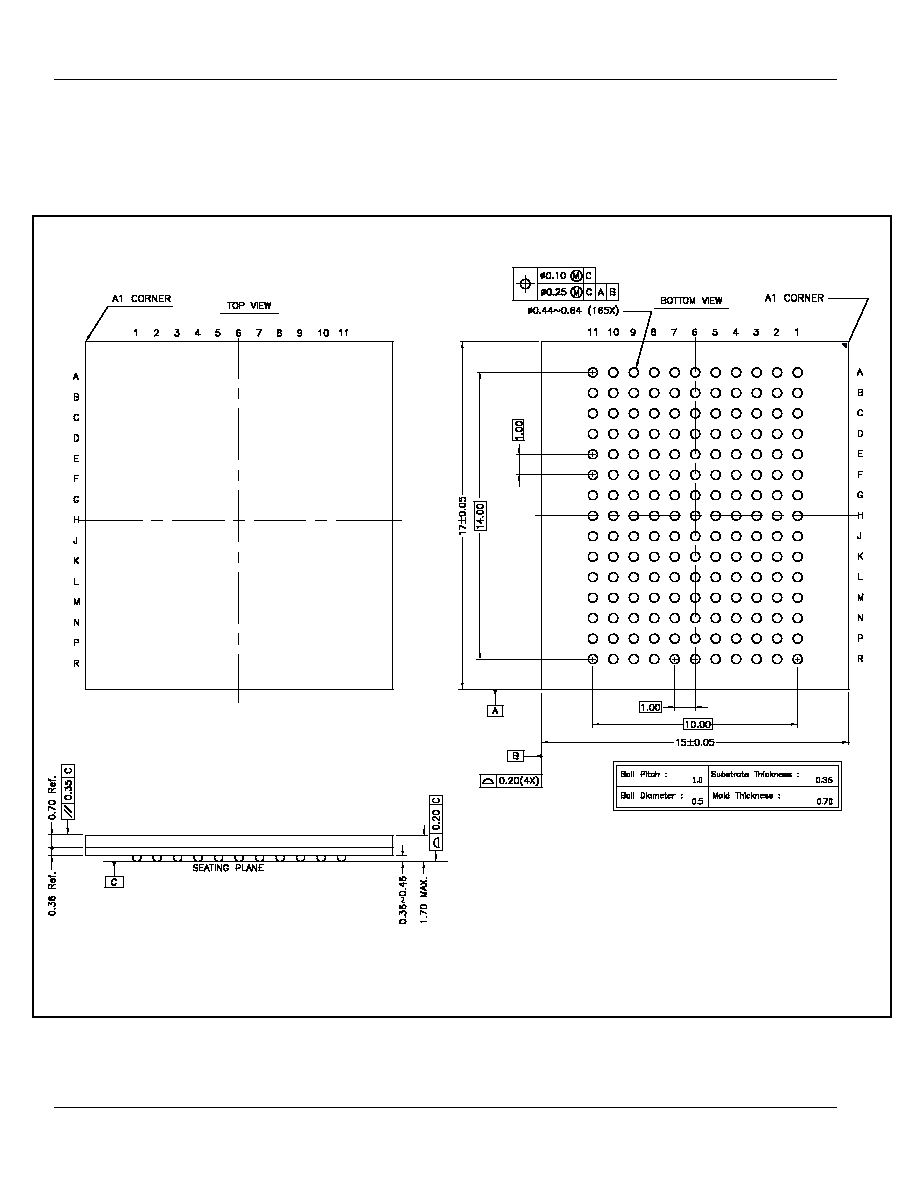
11 x 15 FBGA Dimensions

Integrated Silicon Solution, Inc. -- 1-800-379-4774
27
Rev.
B
0
6/29/06
ISSI
Æ
36 Mb (1M x 36 & 2M x 18)
QUAD (Burst of 2) Synchronous SRAMs
ORDERING INFORMATION
Commercial Range: 0∞C to +70∞C
Speed
Order Part No.
Organization
Package
250 MHz
IS61QDB21M36-250M3
1Mx36
165 BGA
IS61QDB21M36-250M3L
1Mx36
165 BGA, Lead-free
IS61QDB22M18-250M3
2Mx18
165 BGA
IS61QDB22M18-250M3L
2Mx18
165 BGA, Lead-free