
Integrated Silicon Solution, Inc. -- 1-800-379-4774
1
Rev. 00A
04/29/03
IS64LF6436
IS64LF6432
ISSI
Æ
Copyright © 2003 Integrated Silicon Solution, Inc. All rights reserved. ISSI reserves the right to make changes to this specification and its products at any time
without notice. ISSI assumes no liability arising out of the application or use of any information, products or services described herein. Customers are advised to
obtain the latest version of this device specification before relying on any published information and before placing orders for products.
FEATURES
∑ Internal self-timed write cycle
∑ Individual Byte Write Control and Global Write
∑ Clock controlled, registered address, data and
control
∑ Interleaved or linear burst sequence control
using MODE input
∑ Three chip enables for simple depth expansion
and address pipelining
∑ Common data inputs and data outputs
∑ Power-down control by ZZ input
∑ JEDEC 100-Pin TQFP package
∑ Power Supply:
+3.3V V
DD
+3.3V or 2.5V V
DDQ
∑ Control pins mode upon power-up:
≠ MODE in interleave burst mode
≠ ZZ in normal operation mode
∑ Temperature offerings:
Option A1: -40
0
C to +85
0
C
Option A2: -40
0
C to +105
0
C
Option A3: -40
0
C to +125
0
C
DESCRIPTION
The
ISSI
IS64LF6432 and IS64LF6436 are high-speed,
low-power synchronous static RAM designed to provide a
burstable, high-performance, memory. IS64LF6432 is orga-
nized as 65,536 words by 32 bits and IS64LF6436 is
organized as 65,536 words by 36 bits. They are fabricated
with
ISSI
's advanced CMOS technology. The device inte-
grates a 2-bit burst counter, high-speed SRAM core, and
high-drive capability outputs into a single monolithic circuit.
All synchronous inputs pass through registers controlled by
a positive-edge-triggered single clock input.
Write cycles are internally self-timed and are initiated by the
rising edge of the clock input. Write cycles can be from one
to four bytes wide as controlled by the write control inputs.
Separate byte enables allow individual bytes to be written.
BW1
controls DQ1-DQ8,
BW2
controls DQ9-DQ16,
BW3
controls DQ17-DQ24,
BW4
controls DQ25-DQ32, condi-
tioned by
BWE
being LOW. A LOW on
GW
input would
cause all bytes to be written.
Bursts can be initiated with either
ADSP
(Address Status
Processor) or
ADSC
(Address Status Cache Controller)
input pins. Subsequent burst addresses can be generated
internally by the IS64LF6432/36 and controlled by the
ADV
(burst address advance) input pin.
The mode pin is used to select the burst sequence order.
Linear burst is achieved when this pin is tied LOW. Inter-
leave burst is achieved when this pin is tied HIGH or left
floating.
64K x 32, 64Kx36 SYNCHRONOUS
FLOW-THROUGH STATIC RAM
ADVANCE INFORMATION
APRIL 2003
FAST ACCESS TIME
Symbol
Parameter
8.5
10
Unit
t
KQ
Clock Access Time
8.5
10
ns
t
KC
Cycle Time
11
15
ns
Frequency
90
66
MHz
IS64LF6432 IS64LF6436
ISSI
Æ
2
Integrated Silicon Solution, Inc. -- 1-800-379-4774
Rev. 00A
04/29/03
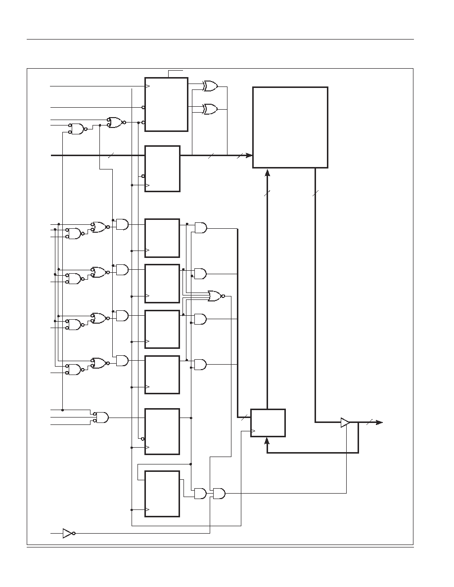
BLOCK DIAGRAM
16
BINARY
COUNTER
A
BW1
(x32/x36)
GW
CLR
CE
CLK
Q0
Q1
MODE
A0'
A0
A1
A1'
CLK
ADV
ADSC
ADSP
14
16
ADDRESS
REGISTER
CE
D
CLK
Q
DQ32-DQ25
BYTE WRITE
REGISTERS
D
CLK
Q
DQ24-DQ17
BYTE WRITE
REGISTERS
D
CLK
Q
DQ16-DQ9
BYTE WRITE
REGISTERS
D
CLK
Q
DQ8-DQ1
BYTE WRITE
REGISTERS
D
CLK
Q
ENABLE
REGISTER
CE
D
CLK
Q
ENABLE
DELAY
REGISTER
D
CLK
Q
BWE
BW4
(x32/x36)
CE
CE2
CE2
BW2
(x32/x36)
BW3
(x32/x36)
64Kx32 / 64Kx36
MEMORY
ARRAY
32
or
36
INPUT
REGISTERS
CLK
32
or
36
OE
4
32 or 36
OE
DATA[32:1]
IS64LF6432 IS64LF6436
ISSI
Æ
Integrated Silicon Solution, Inc. -- 1-800-379-4774
3
Rev. 00A
04/29/03
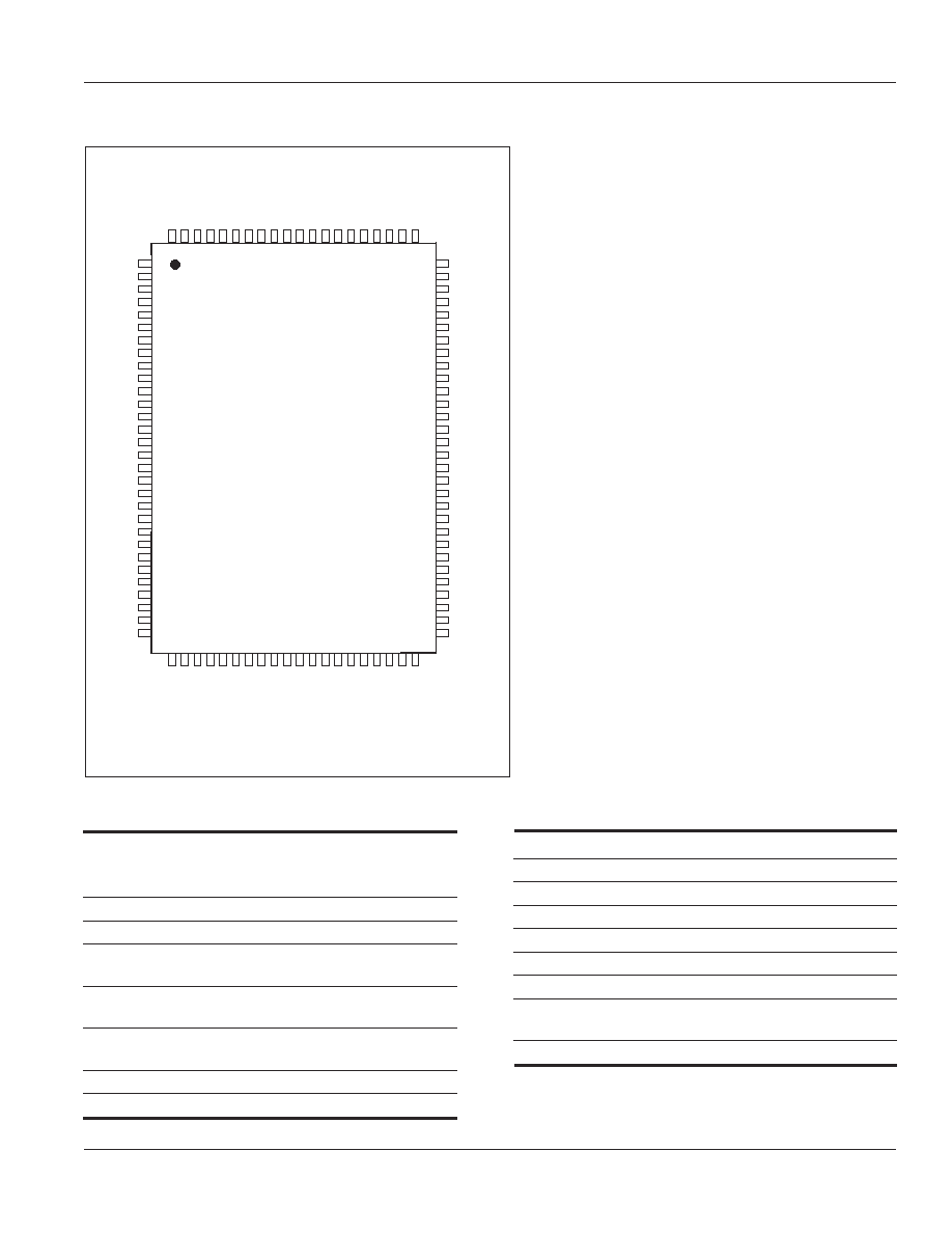
PIN CONFIGURATION
PIN DESCRIPTIONS
A0, A1
Synchronous Address Inputs. These
pins must tied to the two LSBs of the
address bus.
A
Synchronous Address Inputs
CLK
Synchronous Clock
ADSP
Synchronous Processor Address
Status
ADSC
Synchronous Controller Address
Status
ADV
Synchronous Burst Address Ad-
vance
BW1
-
BW4
Individual Byte Write Enable
BWE
Synchronous Byte Write Enable
GW
Synchronous Global Write Enable
CE
,
CE2
, CE2 Synchronous Chip Enable
OE
Output Enable
DQa-DQd
Synchronous Data Input/Output
MODE
Burst Sequence Mode Selection
V
DD
+3.3V Power Supply
GND
Ground
V
DDQ
Isolated Output Buffer Supply: +3.3V
or 2.5V
ZZ
Snooze Enable
NC
DQb
DQb
VDDQ
GND
DQb
DQb
DQb
DQb
GND
VDDQ
DQb
DQb
GND
NC
VDD
ZZ
DQa
DQa
VDDQ
GND
DQa
DQa
DQa
DQa
GND
VDDQ
DQa
DQa
NC
A
A
CE
CE2
BW4
BW3
BW2
BW1
CE2
VDD
GND
CLK
GW
BWE
OE
ADS
C
ADSP
ADV
A
A
NC
DQc
DQc
VDDQ
GND
DQc
DQc
DQc
DQc
GND
VDDQ
DQc
DQc
NC
VDD
NC
GND
DQd
DQd
VDDQ
GND
DQd
DQd
DQd
DQd
GND
VDDQ
DQd
DQd
NC
1
2
3
4
5
6
7
8
9
10
11
12
13
14
15
16
17
18
19
20
21
22
23
24
25
26
27
28
29
30
80
79
78
77
76
75
74
73
72
71
70
69
68
67
66
65
64
63
62
61
60
59
58
57
56
55
54
53
52
51
100 99 98 97 96 95 94 93 92 91 90 89 88 87 86 85 84 83 82 81
31 32 33 34 35 36 37 38 39 40 41 42 43 44 45
MODE
A
A
A
A
A1
A0
NC
NC
GND
VDD
NC
NC
A
A
A
A
A
A
NC
46 47 48 49 50
64K x 32
100-Pin TQFP
IS64LF6432 IS64LF6436
ISSI
Æ
4
Integrated Silicon Solution, Inc. -- 1-800-379-4774
Rev. 00A
04/29/03
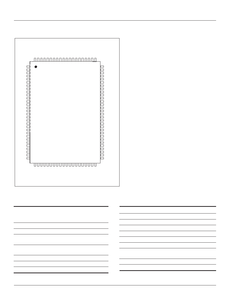
PIN CONFIGURATION
PIN DESCRIPTIONS
A0, A1
Synchronous Address Inputs. These
pins must tied to the two LSBs of the
address bus.
A
Synchronous Address Inputs
CLK
Synchronous Clock
ADSP
Synchronous Processor Address
Status
ADSC
Synchronous Controller Address
Status
ADV
Synchronous Burst Address Advance
BW1
-
BW4
Individual Byte Write Enable
BWE
Synchronous Byte Write Enable
GW
Synchronous Global Write Enable
CE
,
CE2
, CE2 Synchronous Chip Enable
OE
Output Enable
DQa-DQd
Synchronous Data Input/Output
MODE
Burst Sequence Mode Selection
V
DD
+3.3V Power Supply
GND
Ground
V
DDQ
Isolated Output Buffer Supply: +3.3V or
2.5V
ZZ
Snooze Enable
DQPa-DQPd
Parity Data I/O
DQPb
DQb
DQb
VDDQ
GND
DQb
DQb
DQb
DQb
GND
VDDQ
DQb
DQb
GND
NC
VDD
ZZ
DQa
DQa
VDDQ
GND
DQa
DQa
DQa
DQa
GND
VDDQ
DQa
DQa
DQPa
A
A
CE
CE2
BW4
BW3
BW2
BW1
CE2
VDD
GND
CLK
GW
BWE
OE
ADS
C
ADSP
ADV
A
A
DQPc
DQc
DQc
VDDQ
GND
DQc
DQc
DQc
DQc
GND
VDDQ
DQc
DQc
NC
VDD
NC
GND
DQd
DQd
VDDQ
GND
DQd
DQd
DQd
DQd
GND
VDDQ
DQd
DQd
DQPd
1
2
3
4
5
6
7
8
9
10
11
12
13
14
15
16
17
18
19
20
21
22
23
24
25
26
27
28
29
30
80
79
78
77
76
75
74
73
72
71
70
69
68
67
66
65
64
63
62
61
60
59
58
57
56
55
54
53
52
51
100 99 98 97 96 95 94 93 92 91 90 89 88 87 86 85 84 83 82 81
31 32 33 34 35 36 37 38 39 40 41 42 43 44 45
MODE
A
A
A
A
A1
A0
NC
NC
GND
VDD
NC
NC
A
A
A
A
A
A
NC
46 47 48 49 50
64K x 36
100-Pin TQFP

IS64LF6432 IS64LF6436
ISSI
Æ
Integrated Silicon Solution, Inc. -- 1-800-379-4774
5
Rev. 00A
04/29/03
TRUTH TABLE
Address
Operation
Used
CE
CE
CE
CE
CE
CE2
CE2
CE2
CE2
CE2
CE2
ADSP
ADSP
ADSP
ADSP
ADSP ADSC
ADSC
ADSC
ADSC
ADSC
ADV
ADV
ADV
ADV
ADV WRITE
WRITE
WRITE
WRITE
WRITE
OE
OE
OE
OE
OE
DQ
Deselected, Power-down
None
H
X
X
X
L
X
X
X
High-Z
Deselected, Power-down
None
L
X
H
L
X
X
X
X
High-Z
Deselected, Power-down
None
L
L
X
L
X
X
X
X
High-Z
Deselected, Power-down
None
X
X
H
H
L
X
X
X
High-Z
Deselected, Power-down
None
X
L
X
H
L
X
X
X
High-Z
Read Cycle, Begin Burst
External
L
H
L
L
X
X
X
X
Q
Read Cycle, Begin Burst
External
L
H
L
H
L
X
Read
X
Q
Write Cycle, Begin Burst
External
L
H
L
H
L
X
Write
X
D
Read Cycle, Continue Burst
Next
X
X
X
H
H
L
Read
L
Q
Read Cycle, Continue Burst
Next
X
X
X
H
H
L
Read
H
High-Z
Read Cycle, Continue Burst
Next
H
X
X
X
H
L
Read
L
Q
Read Cycle, Continue Burst
Next
H
X
X
X
H
L
Read
H
High-Z
Write Cycle, Continue Burst
Next
X
X
X
H
H
L
Write
X
D
Write Cycle, Continue Burst
Next
H
X
X
X
H
L
Write
X
D
Read Cycle, Suspend Burst
Current
X
X
X
H
H
H
Read
L
Q
Read Cycle, Suspend Burst
Current
X
X
X
H
H
H
Read
H
High-Z
Read Cycle, Suspend Burst
Current
H
X
X
X
H
H
Read
L
Q
Read Cycle, Suspend Burst
Current
H
X
X
X
H
H
Read
H
High-Z
Write Cycle, Suspend Burst
Current
X
X
X
H
H
H
Write
X
D
Write Cycle, Suspend Burst
Current
H
X
X
X
H
H
Write
X
D
PARTIAL TRUTH TABLE
Function
GW
GW
GW
GW
GW
BWE
BWE
BWE
BWE
BWE
BW1
BW1
BW1
BW1
BW1
BW2
BW2
BW2
BW2
BW2
BW3
BW3
BW3
BW3
BW3
BW4
BW4
BW4
BW4
BW4
Read
H
H
X
X
X
X
Read
H
L
H
H
H
H
Write Byte 1
H
L
L
H
H
H
Write All Bytes
H
L
L
L
L
L
Write All Bytes
L
X
X
X
X
X