Integrated Silicon Solution, Inc. -- 1-800-379-4774
1
Rev. 00A
08/11/05
ISSI
Æ
IS61(64)LF12832A IS64VF12832A
IS61(64)LF12836A IS61(64)VF12836A
IS61(64)LF25618A IS61(64)VF25618A
Copyright © 2005 Integrated Silicon Solution, Inc. All rights reserved. ISSI reserves the right to make changes to this specification and its products at any time
without notice. ISSI assumes no liability arising out of the application or use of any information, products or services described herein. Customers are advised to
obtain the latest version of this device specification before relying on any published information and before placing orders for products.
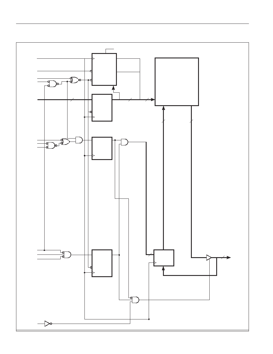
FEATURES
∑ Internal self-timed write cycle
∑ Individual Byte Write Control and Global Write
∑ Clock controlled, registered address, data and
control
∑ Burst sequence control using MODE input
∑ Three chip enable option for simple depth expan-
sion and address pipelining
∑ Common data inputs and data outputs
∑ Auto Power-down during deselect
∑ Single cycle deselect
∑ Snooze MODE for reduced-power standby
∑ Power Supply
LF: V
DD
3.3V + 5%, V
DDQ
3.3V/2.5V + 5%
VF: V
DD
2.5V -5% +10%, V
DDQ
2.5V -5% +10%
∑ JEDEC 100-Pin TQFP, 119-pin PBGA, and
165-pin PBGA packages
∑ Automotive temperature available
∑ Lead-free available
PRELIMINARY INFORMATION
AUGUST 2005
128K x 32, 128K x 36, 256K x 18
4 Mb SYNCHRONOUS FLOW-THROUGH
STATIC RAM
DESCRIPTION
The
ISSI
IS61(64)LF12832A, IS64VF12832A,
IS61(64)LF/VF12836A and IS61(64)LF/VF25618A are
high-speed, low-power synchronous static RAMs designed
to provide burstable, high-performance memory for commu-
nication and networking applications. The
IS61(64)LF12832A is organized as 131,072 words by 32
bits. The IS61(64)LF/VF12836A is organized as 131,072
words by 36 bits. The IS61(64)LF/VF25618A is organized
as 262,144 words by 18 bits. Fabricated with
ISSI
's
advanced CMOS technology, the device integrates a 2-bit
burst counter, high-speed SRAM core, and high-drive
capability outputs into a single monolithic circuit. All syn-
chronous inputs pass through registers controlled by a
positive-edge-triggered single clock input.
Write cycles are internally self-timed and are initiated by
the rising edge of the clock input. Write cycles can be one
to four bytes wide as controlled by the write control inputs.
Separate byte enables allow individual bytes to be written.
Byte write operation is performed by using byte write
enable (
BWE
) input combined with one or more individual
byte write signals (
BWx
). In addition, Global Write (
GW
) is
available for writing all bytes at one time, regardless of the
byte write controls.
Bursts can be initiated with either
ADSP
(Address Status
Processor) or
ADSC
(Address Status Cache Controller)
input pins. Subsequent burst addresses can be generated
internally and controlled by the
ADV
(burst address ad-
vance) input pin.
The mode pin is used to select the burst sequence order,
Linear burst is achieved when this pin is tied LOW.
Interleave burst is achieved when this pin is tied HIGH or
left floating.
FAST ACCESS TIME
Symbol
Parameter
-6.5
-7.5
Units
t
KQ
Clock Access Time
6.5
7.5
ns
t
KC
Cycle Time
7.5
8.5
ns
Frequency
133
117
MHz
4
Integrated Silicon Solution, Inc. -- 1-800-379-4774
Rev. 00A
08/11/05
ISSI
Æ
IS61(64)LF12832A, IS61(64)LF12836A, IS61(64)LF25618A
IS64VF12832A, IS61(64)VF12836A, IS61(64)VF25618A
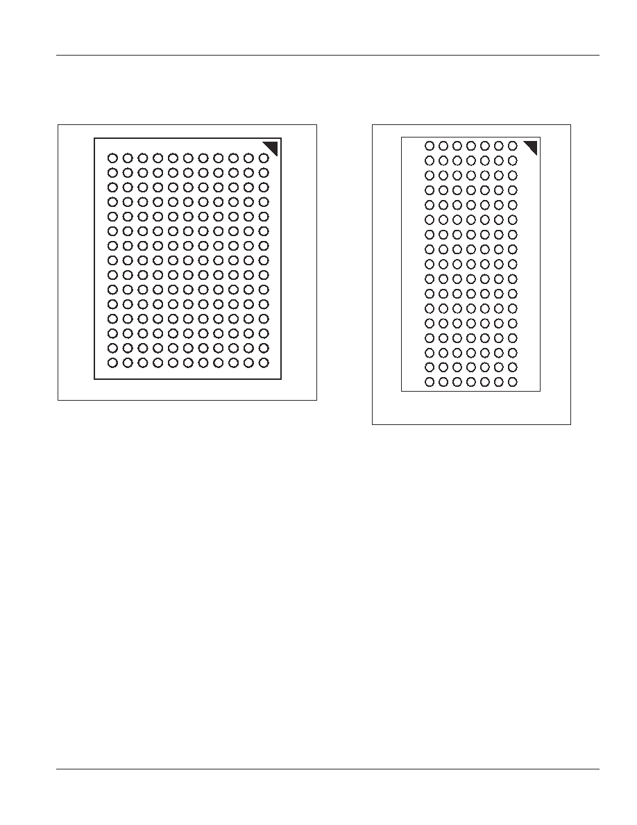
119 BGA PACKAGE PIN CONFIGURATION
128K
X
36
(TOP VIEW)
PIN DESCRIPTIONS
1
2
3
4
5
6
7
A
V
DDQ
A
A
ADSP
A
A
V
DDQ
B
NC
CE2
A
ADSC
A
CE2
NC
C
NC
A
A
V
DD
A
A
NC
D
DQc
DQPc
Vss
NC
Vss
DQPb
DQb
E
DQc
DQc
Vss
CE
Vss
DQb
DQb
F
V
DDQ
DQc
Vss
OE
Vss
DQb
V
DDQ
G
DQc
DQc
BWc
ADV
BWb
DQb
DQb
H
DQc
DQc
Vss
GW
Vss
DQb
DQb
J
V
DDQ
V
DD
NC
V
DD
NC
V
DD
V
DDQ
K
DQd
DQd
Vss
CLK
Vss
DQa
DQa
L
DQd
DQd
BWd
NC
BWa
DQa
DQa
M
V
DDQ
DQd
Vss
BWE
Vss
DQa
V
DDQ
N
DQd
DQd
Vss
A
1
*
Vss
DQa
DQa
P
DQd
DQPd
Vss
A
0
*
Vss
DQPa
DQa
R
NC
A
MODE
V
DD
NC
A
NC
T
NC
NC
A
A
A
NC
ZZ
U
V
DDQ
NC
NC
NC
NC
NC
V
DDQ
Symbol
Pin Name
A
Address Inputs
A0, A1
Synchronous Burst Address Inputs
ADV
Synchronous Burst Address
Advance
ADSP
Address Status Processor
ADSC
Address Status Controller
GW
Global Write Enable
CLK
Synchronous Clock
CE
, CE2,
CE2
Synchronous Chip Select
BW
x (x=a-d)
Synchronous Byte Write Controls
BWE
Byte Write Enable
Symbol
Pin Name
OE
Output Enable
ZZ
Power Sleep Mode
MODE
Burst Sequence Selection
NC
No Connect
DQa-DQd
Data Inputs/Outputs
DQPa-Pd
Output Power Supply
V
DD
Power Supply
V
DDQ
Output Power Supply
Vss
Ground
Note: * A
0
and A
1
are the two least significant bits (LSB) of the address field and set the internal burst counter if burst is desired.
Integrated Silicon Solution, Inc. -- 1-800-379-4774
5
Rev. 00A
08/11/05
ISSI
Æ
IS61(64)LF12832A, IS61(64)LF12836A, IS61(64)LF25618A
IS64VF12832A, IS61(64)VF12836A, IS61(64)VF25618A
119 BGA PACKAGE PIN CONFIGURATION
256K
X
18
(TOP VIEW)
PIN DESCRIPTIONS
Note: * A
0
and A
1
are the two least significant bits (LSB) of the address field and set the internal burst counter if burst is desired.
1
2
3
4
5
6
7
A
V
DDQ
A
A
ADSP
A
A
V
DDQ
B
NC
CE2
A
ADSC
A
CE2
NC
C
NC
A
A
V
DD
A
A
NC
D
DQb
NC
Vss
NC
Vss
DQPa
NC
E
NC
DQb
Vss
CE
Vss
NC
DQa
F
V
DDQ
NC
Vss
OE
Vss
DQa
V
DDQ
G
NC
DQb
BWb
ADV
Vss
NC
DQa
H
DQb
NC
Vss
GW
Vss
DQa
NC
J
V
DDQ
V
DD
NC
V
DD
NC
V
DD
V
DDQ
K
NC
DQb
Vss
CLK
Vss
NC
DQa
L
DQb
NC
Vss
NC
BWa
DQa
NC
M
V
DDQ
DQb
Vss
BWE
Vss
NC
V
DDQ
N
DQb
NC
Vss
A
1
*
Vss
DQa
NC
P
NC
DQPb
Vss
A
0
*
Vss
NC
DQa
R
NC
A
MODE
V
DD
NC
A
NC
T
NC
A
A
NC
A
A
ZZ
U
V
DDQ
NC
NC
NC
NC
NC
V
DDQ
Symbol
Pin Name
A
Address Inputs
A0, A1
Synchronous Burst Address Inputs
ADV
Synchronous Burst Address
Advance
ADSP
Address Status Processor
ADSC
Address Status Controller
GW
Global Write Enable
CLK
Synchronous Clock
CE
, CE2,
CE2
Synchronous Chip Select
BW
x (x=a,b)
Synchronous Byte Write Controls
BWE
Byte Write Enable
Symbol
Pin Name
OE
Output Enable
ZZ
Power Sleep Mode
MODE
Burst Sequence Selection
NC
No Connect
DQa-DQb
Data Inputs/Outputs
DQPa-Pb
Output Power Supply
V
DD
Power Supply
V
DDQ
Output Power Supply
Vss
Ground