Integrated Silicon Solution, Inc. -- www.issi.com --
1-800-379-4774
1
Rev. C
01/24/05
ISSI
Æ
Copyright © 2005 Integrated Silicon Solution, Inc. All rights reserved. ISSI reserves the right to make changes to this specification and its products at any time without notice. ISSI assumes no liability
arising out of the application or use of any information, products or services described herein. Customers are advised to obtain the latest version of this device specification before relying on any
published information and before placing orders for products.
IS62C1024AL
IS65C1024AL
DESCRIPTION
The
ISSI
IS62C1024AL/IS65C1024AL is a low power, 131,072-
word by 8-bit CMOS static RAM. It is fabricated using high-
performance CMOS technology. This highly reliable pro-
cess coupled with innovative circuit design techniques,
yields higher performance and low power consumption
devices.
When
CE1
is HIGH or CE2 is LOW (deselected), the device
assumes a standby mode at which the power dissipation
can be reduced by using CMOS input levels.
Easy memory expansion is provided by using two Chip
Enable inputs,
CE1
and CE2. The active LOW Write Enable
(
WE
) controls both writing and reading of the memory.
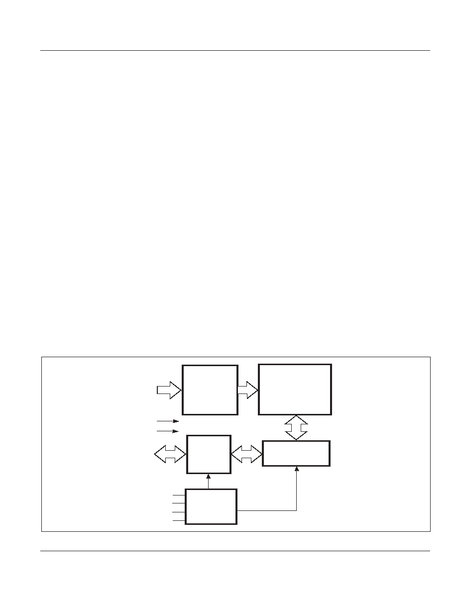
FUNCTIONAL BLOCK DIAGRAM
128K x 8 LOW POWER CMOS
STATIC RAM
FEATURES
∑ High-speed access time: 35, 45 ns
∑ Low active power: 100 mW (typical)
∑ Low standby power: 20 µW (typical) CMOS
standby
∑ Output Enable (
OE
) and two Chip Enable
(
CE1
and CE2) inputs for ease in applications
∑ Fully static operation: no clock or refresh
required
∑ TTL compatible inputs and outputs
∑ Single 5V (±10%) power supply
∑ Commercial, Industrial, and Automotive tem-
perature ranges available
∑ Standard Pin Configuration:
--
32-pin SOP/ 32-pin TSOP (Type 1)
∑ Lead free available
A0-A16
CE1
OE
WE
128K x 8
MEMORY ARRAY
DECODER
COLUMN I/O
CONTROL
CIRCUIT
GND
V
DD
I/O
DATA
CIRCUIT
I/O0-I/O7
CE2
JANUARY 2005
2
Integrated Silicon Solution, Inc. -- www.issi.com --
1-800-379-4774
Rev. C
01/24/05
ISSI
Æ
IS62C1024AL
IS65C1024AL
TRUTH TABLE
Mode
WE
WE
WE
WE
WE
CE1
CE1
CE1
CE1
CE1
CE2
OE
OE
OE
OE
OE
I/O Operation
V
DD
Current
Not Selected
X
H
X
X
High-Z
I
SB
1
, I
SB
2
(Power-down)
X
X
L
X
High-Z
I
SB
1
, I
SB
2
Output Disabled
H
L
H
H
High-Z
I
CC
Read
H
L
H
L
D
OUT
I
CC
Write
L
L
H
X
D
IN
I
CC
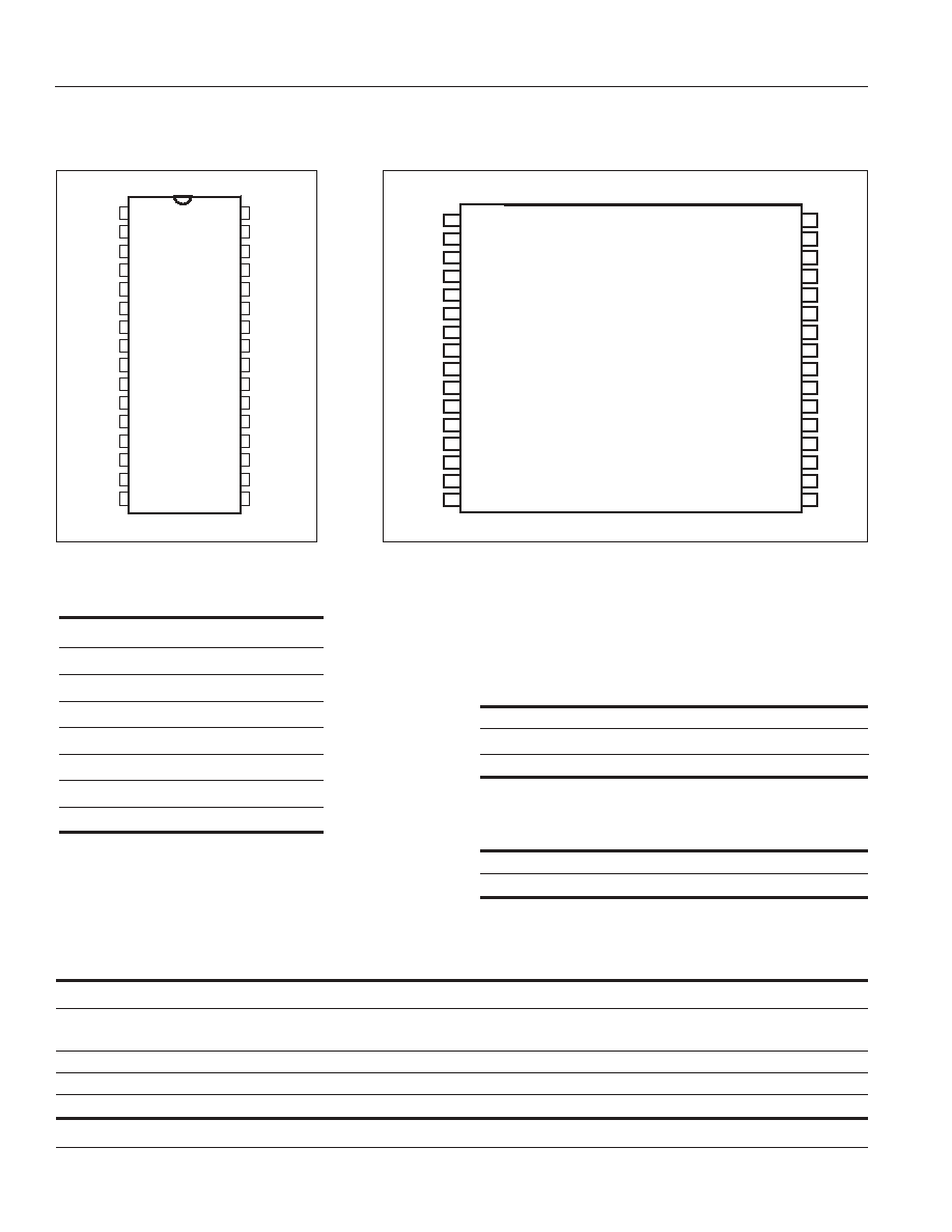
PIN CONFIGURATION
32-Pin SOP
PIN DESCRIPTIONS
A0-A16
Address Inputs
CE1
Chip Enable 1 Input
CE2
Chip Enable 2 Input
OE
Output Enable Input
WE
Write Enable Input
I/O0-I/O7
Input/Output
V
DD
Power
GND
Ground
PIN CONFIGURATION
32-Pin TSOP (Type 1)
1
2
3
4
5
6
7
8
9
10
11
12
13
14
15
16
32
31
30
29
28
27
26
25
24
23
22
21
20
19
18
17
NC
A16
A14
A12
A7
A6
A5
A4
A3
A2
A1
A0
I/O0
I/O1
I/O2
GND
V
DD
A15
CE2
WE
A13
A8
A9
A11
OE
A10
CE1
I/O7
I/O6
I/O5
I/O4
I/O3
1
2
3
4
5
6
7
8
9
10
11
12
13
14
15
16
32
31
30
29
28
27
26
25
24
23
22
21
20
19
18
17
A11
A9
A8
A13
WE
CE2
A15
V
DD
NC
A16
A14
A12
A7
A6
A5
A4
OE
A10
CE1
I/O7
I/O6
I/O5
I/O4
I/O3
GND
I/O2
I/O1
I/O0
A0
A1
A2
A3
OPERATING RANGE (IS65C1024AL)
Range
Ambient Temperature
V
DD
Automotive
-40∞C to +125∞C
5V ± 10%
OPERATING RANGE (IS62C1024AL)
Range
Ambient Temperature
V
DD
Commercial
0∞C to +70∞C
5V ± 10%
Industrial
-40∞C to +85∞C
5V ± 10%
Integrated Silicon Solution, Inc. -- www.issi.com --
1-800-379-4774
3
Rev. C
01/24/05
ISSI
Æ
IS62C1024AL
IS65C1024AL
ABSOLUTE MAXIMUM RATINGS
(1)
Symbol
Parameter
Value
Unit
V
TERM
Terminal Voltage with Respect to GND
≠0.5 to +7.0
V
T
STG
Storage Temperature
≠65 to +125
∞C
P
T
Power Dissipation
1.0
W
I
OUT
DC Output Current (LOW)
20
mA
Notes:
1. Stress greater than those listed under ABSOLUTE MAXIMUM RATINGS may cause permanent damage to the device. This is a
stress rating only and functional operation of the device at these or any other conditions above those indicated in the operational
sections of this specification is not implied. Exposure to absolute maximum rating conditions for extended periods may affect
reliability.
CAPACITANCE
(1,2)
Symbol
Parameter
Conditions
Max.
Unit
C
IN
Input Capacitance
V
IN
= 0V
6
pF
C
OUT
Output Capacitance
V
OUT
= 0V
8
pF
Notes:
1. Tested initially and after any design or process changes that may affect these parameters.
2. Test conditions: T
A
= 25∞C, f = 1 MHz, V
DD
= 5.0V.
DC ELECTRICAL CHARACTERISTICS
(Over Operating Range)
Symbol Parameter
Test Conditions
Options
Min.
Max.
Unit
V
OH
Output HIGH Voltage
V
DD
= Min., I
OH
= ≠1.0 mA
2.4
--
V
V
OL
Output LOW Voltage
V
DD
= Min., I
OL
= 2.1 mA
--
0.4
V
V
IH
Input HIGH Voltage
2.2
V
DD
+ 0.5
V
V
IL
Input LOW Voltage
(1)
-0.5
0.8
V
I
LI
Input Leakage
GND
V
IN
V
DD
Com.
-1
1
µA
Ind.
-2
2
Auto.
-5
5
I
LO
Output Leakage
GND
V
OUT
V
DD
Com.
-1
1
µA
CE1
= V
IH
, or
Ind.
-2
2
CE2 = V
IL
, or
OE
= V
IH
or
Auto.
-5
5
WE
= V
IL
4
Integrated Silicon Solution, Inc. -- www.issi.com --
1-800-379-4774
Rev. C
01/24/05
ISSI
Æ
IS62C1024AL
IS65C1024AL
READ CYCLE SWITCHING CHARACTERISTICS
(1)
(Over Operating Range)
-35 ns
-45 ns
Symbol
Parameter
Min.
Max.
Min.
Max.
Unit
t
RC
Read Cycle Time
35
--
45
--
ns
t
AA
Address Access Time
--
35
--
45
ns
t
OHA
Output Hold Time
3
--
3
--
ns
t
ACE
1
CE1
Access Time
--
35
--
45
ns
t
ACE
2
CE2 Access Time
--
35
--
45
ns
t
DOE
OE
Access Time
--
10
--
20
ns
t
LZOE
(2)
OE
to Low-Z Output
3
--
5
--
ns
t
HZOE
(2)
OE
to High-Z Output
0
10
0
15
ns
t
LZCE
1
(2)
CE1
to Low-Z Output
3
--
5
--
ns
t
LZCE
2
(2)
CE2 to Low-Z Output
3
--
5
--
ns
t
HZCE
(2)
CE1
or CE2 to High-Z Output
0
10
0
15
ns
Notes:
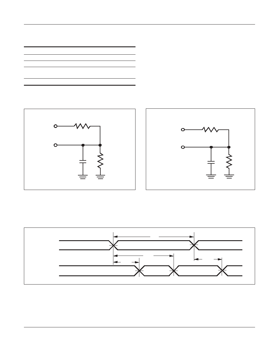
1. Test conditions assume signal transition times of 5 ns or less, timing reference levels of 1.5V, input pulse levels of
0.6 to 2.4V and output loading specified in Figure 1a.
2. Tested with the load in Figure 1b. Transition is measured ±500 mV from steady-state voltage. Not 100% tested.
IS62C1024AL/IS65C1024AL
POWER SUPPLY CHARACTERISTICS
(1)
(Over Operating Range)
-35 ns -45 ns
Symbol Parameter
Test Conditions
Min.
Max.
Min.
Max.
Unit
I
CC
Average operating
CE1
= V
IL
, CE2 = V
IH
Com.
--
25
mA
Current
V
IN
= V
IH
or V
IL
,
Ind.
--
30
I
I/O
= 0 mA
Auto.
--
35
I
CC
1
V
DD
Dynamic Operating
V
DD
= Max.,
CE1
= V
IL
Com.
--
30
mA
Supply Current
I
OUT
= 0 mA, f = f
MAX
Ind.
--
35
V
IN
= V
IH
or V
IL
Auto.
--
40
CE2 = V
IH
typ.
(2)
--
20
I
SB
1
TTL Standby Current
V
DD
= Max.,
Com.
--
1
mA
(TTL Inputs)
V
IN
= V
IH
or V
IL
,
CE1
V
IH
,
Ind.
--
1.5
or CE2
V
IL
, f = 0
Auto.
--
2
I
SB
2
CMOS Standby
V
DD
= Max.,
Com.
--
5
µA
Current (CMOS Inputs)
CE1
V
DD
≠ 0.2V, or
Ind.
--
10
CE2
0.2V, V
IN
V
DD
≠ 0.2V,
Auto.
--
15
or V
IN
V
SS
+ 0.2V, f = 0
typ.
(2)
--
4
Note:
1. At f = f
MAX
, address and data inputs are cycling at the maximum frequency, f = 0 means no input lines change.
2. Typical Values are measured at V
DD
= 5V, T
A
= 25
o
C and not 100% tested.