IS71VPCF16
X
S04
ISSI
Æ
Integrated Silicon Solution, Inc. -- www.issi.com --
1-800-379-4774
PRELIMINARY INFORMATION Rev. 00C
06/14/02
Copyright © 2002 Integrated Silicon Solution, Inc. All rights reserved. ISSI reserves the right to make changes to this specification and its products at any time
without notice. ISSI assumes no liability arising out of the application or use of any information, products or services described herein. Customers are advised to
obtain the latest version of this device specification before relying on any published information and before placing orders for products.
3.0 Volt-Only Flash & SRAM COMBO with Stacked Multi-Chip
Package (MCP) -- 16 Mbit Simultaneous Operation Flash
Memory and 4 Mbit Static RAM
MCP FEATURES
∑
Power supply voltage 2.7V to 3.3V
∑
High performance:
Flash: 85ns maximum access time
SRAM: 85ns maximum access time
∑
Package: 69-ball BGA
∑
Operating Temperature: -25C to +85C
FLASH FEATURES
∑
Power Dissipation:
Read Current at 1 Mhz: 7 mA maximum
Read Current at 5 Mhz: 18 mA maximum
Sleep Mode: 5
µ
A maximum
∑
Simultaneous Read and Write Operations:
Zero latency between read and write operations; Data
can be programmed or erased in one bank while data
is simultaneously being read from the other bank
∑
Low-Power Mode:
A period of no activity causes flash to enter a low-
power state
∑
Erase Suspend/Resume:
Suspends of erase activity to allow a read in the
same bank.
∑
Sector Erase Architecture:
8 words of 4k size and 31 words of 32K size (16 Mbit)
Any combination of sectors, or the entire flash can
be simultaneously erased
∑
Erase Algorithms:
Automatically preprograms/erases the flash memory
entirely, or by sector
∑
Program Algorithms:
Automatically writes and verifies data at specified
address
∑
Hidden ROM Region:
64KB with a Factory-serialized secure electronic
serial number (ESN), which is accessible through a
command sequence
∑
Data Polling and Toggle Bit:
Allow for detection of program or erase cycle
completion
∑
Ready-Busy output (RY/
BY
):
Detection of program
or erase cycle completion
∑
Over 100,000 write/erase cycles
∑
Low supply voltage (Vccf
2.5V) inhibits writes
∑
WP
/ACC input pin:
If V
IL
, allows protection of boot sectors
If V
IH
, allows removal of boot sector protection
If Vacc, program time is reduced by 40%
∑
Boot sector: Top or Bottom
SRAM FEATURES (4 Mb density)
∑
Power Dissipation:
Operating: 40 mA maximum
Standby: 7 µA maximum
∑
Chip Selects:
CE1
s, CE2s
∑
Power down feature using
CE1s
, or CE2s
∑
Data retention supply voltage: 1.5 to 3.3 volt
∑
Byte data control:
LB
s (DQ0≠DQ7),
UB
s
(DQ8≠DQ15) -- in x16 mode
GENERAL DESCRIPTION
The flash and SRAM MCP is available in 16 Mbit Flash/4
Mbit SRAM having a data bus of either x8 or x16. The 16
Mbit flash is composed of 1,048,576 words of 16 bits or
2,097,152 bytes of 8 bits. The 4Mb SRAM has 262,144
words of 16 bits or 524,288 bytes of 8 bits. Data lines DQ0-
DQ7 handle the x8 format, while lines DQ0-DQ15 handle
the x16 format.
The package uses a 3.0V power supply for all operations.
No other source is required for program and erase opera-
tions. The flash can be programmed in system using this
3.0V supply, or can be programmed in a standard EPROM
programmer.
The 16 Mbit flash/4 Mbit SRAM is offered in a 69-ball BGA
package. The flash is compatible with the JEDEC Flash
command set standard . The flash access time is 85ns and
the SRAM access time is 85ns.
The Flash architecture is composed of two banks which
allows simultaneous operation on each. Optimized per-
formance can be achieved by first initializing a program or
erase function in one bank, then immediately starting a
read from the other bank. Both operations would then be
operating simultaneously, with zero latency.
PRELIMINARY INFORMATION
JUNE 2002
IS71VPCF16
X
S04
ISSI
Æ
4
Integrated Silicon Solution, Inc. -- www.issi.com --
1-800-379-4774
PRELIMINARY INFORMATION
Rev. 00C
06/14/02
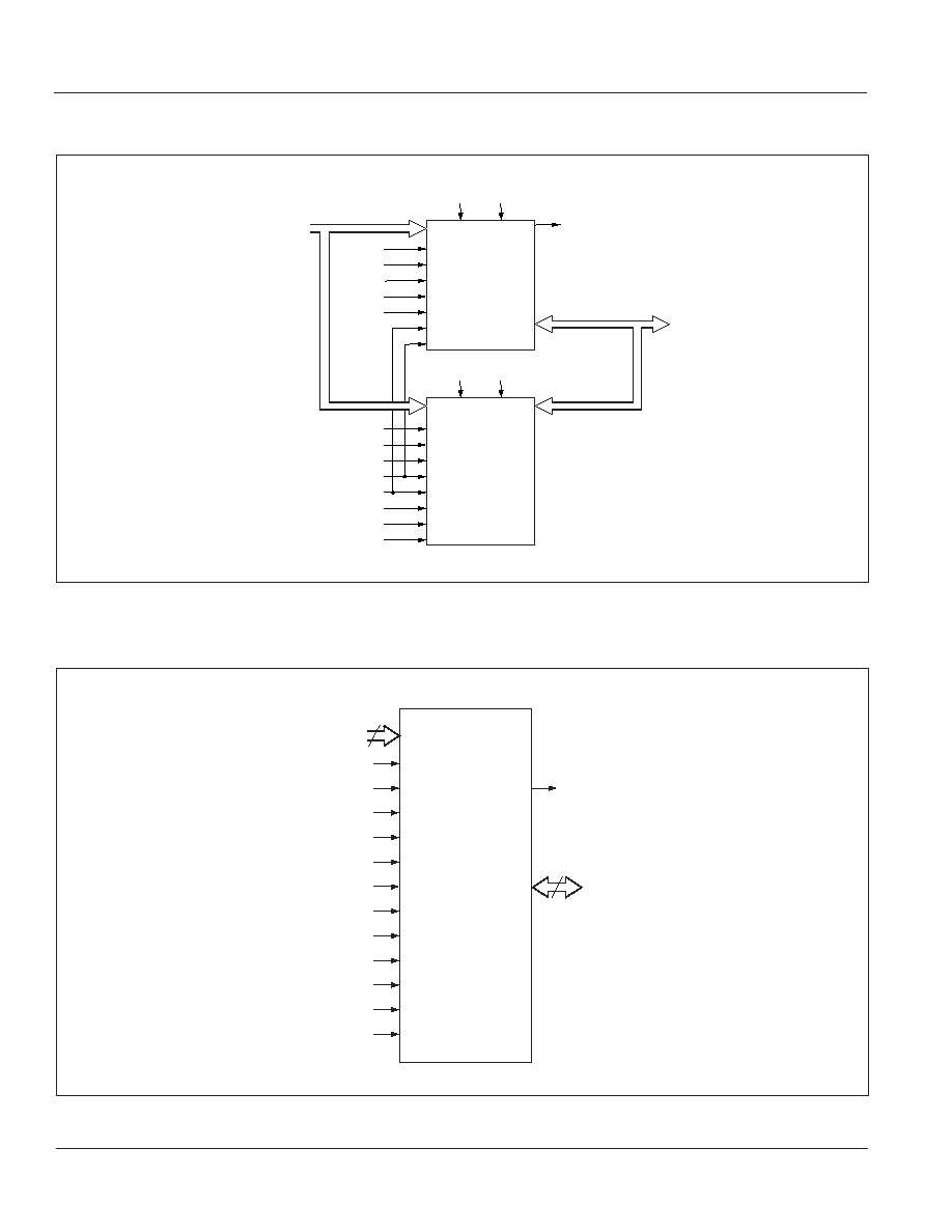
PIN DESCRIPTIONS
A0-A17
Address Inputs, Common
A18-A19, A-1
Address Inputs, Flash
DQ0-DQ15/A-1
Data Inputs/Outputs
RESET
Reset
CE1
s, CE2s
Chip Selects, SRAM
I/Of
I/O Configuration, Flash
CE
f
Chip Enable Input, Flash
OE
Output Enable Input
WE
Write Enable Input
I/Os
I/O Configuration, SRAM
LB
s
Lower-byte Control(DQ0-DQ7), SRAM
UB
s
Upper-byte Control (DQ8-DQ15), SRAM
WP
/ACC
Write Protect/Acceleration Pin, Flash
RY/
BY
Ready/Busy Output
SA
High Order Address Pin, SRAM (x8)
NC
No Connection
Vccf
Power, Flash
Vccs
Power, SRAM
GND
Ground
1234
1234
1234
1234
Shared
Flash only
SRAM only
1234567890123
1234567890123
1234567890123
1234567890123
1234567890123
1234567890123
123456789012345
123456789012345
123456789012345
123456789012345
123456789012345
123456789012345
12345678901234
12345678901234
12345678901234
12345678901234
12345678901234
12345678901234
12345678901234
123456789012345
123456789012345
123456789012345
123456789012345
123456789012345
123456789012345
12345678901234
12345678901234
12345678901234
12345678901234
12345678901234
12345678901234
12345678901234
12345678901234
12345678901234
12345678901234
12345678901234
12345678901234
12345678901234
12345678901234
12345678901234
12345678901234
12345678901234
12345678901234
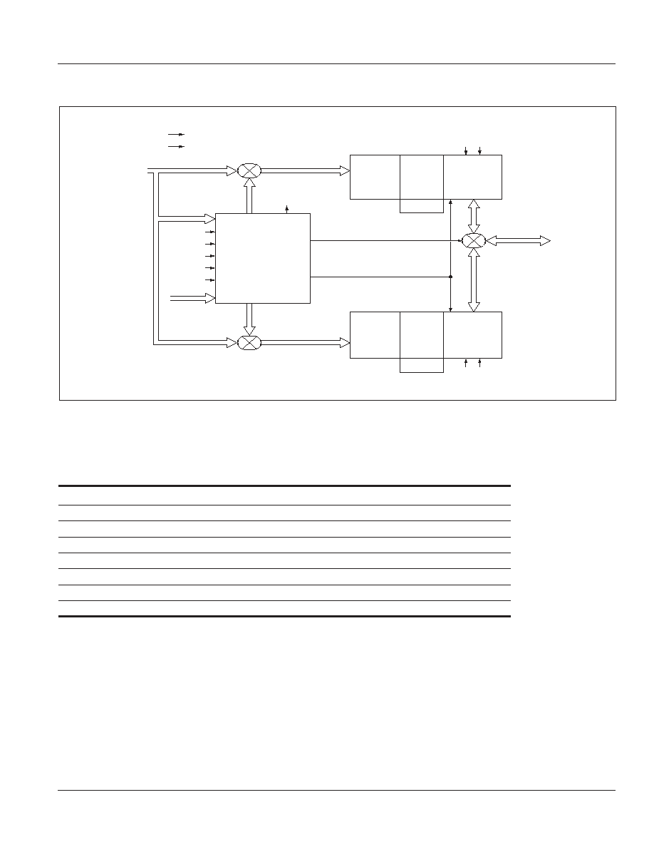
PIN CONFIGURATION
(16 Mb Flash and 4 Mb SRAM)
69 BALL FBGA (Top View)
1
2
3
4
5
6
7
8
9
10
A
NC
NC
NC
NC
B
NC
A7
LB
WP
/ACC
WE
A8
A11
C
A3
A6
UB
RESET
CE2s
A19
A12
A15
D
A2
A5
A18
RY/
BY
NC
A9
A13
NC
E
NC
A1
A4
A17
A10
A14
NC
NC
F
NC
A0
GND
DQ1
DQ6
SA
A16
NC
G
CE
f
OE
DQ9
DQ3
DQ4
DQ13
DQ15/A-1
I/Of
H
CE1
s
DQ0
DQ10
V
CC
f
V
CC
s
DQ12
DQ7
GND
J
DQ8
DQ2
DQ11
I/Os
DQ5
DQ14
K
NC
NC
NC
NC

IS71VPCF16
X
S04
ISSI
Æ
Integrated Silicon Solution, Inc. -- www.issi.com --
1-800-379-4774
5
PRELIMINARY INFORMATION
Rev. 00C
06/14/02
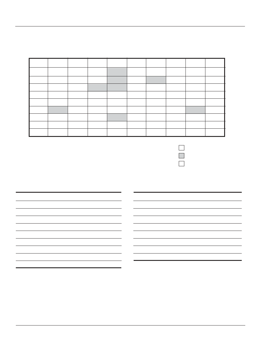
OPERATION
(1,3)
CE
f
CE
1s CE2s
OE
WE
SA
(6)
LB
s
UB
s
DQ
0-
DQ
7
DQ
8
-DQ
15
RESET WP
/ACC
(5)
Full Standby
H
H
X
X
X
X
X
X
High-Z
High-Z
H
X
H
X
L
X
X
X
X
X
High-Z
High-Z
H
X
Output Disable
H
L
H
H
H
X
X
X
High-Z
High-Z
H
X
H
L
H
X
X
X
H
H
High-Z
High-Z
H
X
L
H
X
H
H
X
X
X
High-Z
High-Z
H
X
L
X
L
H
H
X
X
X
High-Z
High-Z
H
X
Read from Flash
(2)
L
H
X
L
H
X
X
X
D
OUT
D
OUT
H
X
L
X
L
L
H
X
X
X
D
OUT
D
OUT
H
X
Write to Flash
L
H
X
H
L
X
X
X
D
IN
D
IN
H
X
L
X
L
H
L
X
X
X
D
IN
D
IN
H
X
Read from SRAM
H
L
H
L
H
X
L
L
D
OUT
D
OUT
H
X
H
L
H
L
H
X
H
L
High-Z
D
OUT
H
X
H
L
H
L
H
X
L
H
D
OUT
High-Z
H
X
Write to SRAM
H
L
H
X
L
X
L
L
D
IN
D
IN
H
X
H
L
H
X
L
X
H
L
High-Z
D
IN
H
X
H
L
H
X
L
X
L
H
D
IN
High-Z
H
X
Temporary Sector
X
X
X
X
X
X
X
X
X
X
V
ID
(8)
X
Group Unprotection
(4)
Flash Hardware
X
H
X
X
X
X
X
X
High-Z
High-Z
L
X
Reset
X
X
L
X
X
X
X
X
High-Z
High-Z
L
X
Boot Block Sector
X
X
X
X
X
X
X
X
X
X
X
L
Write Protection
Notes:
1. Any operations not indicated this column are inhibited.
2.
WE
can be VIL if
OE
is VIL,
OE
at VIH initiates the write operations.
3. Do not apply
CE
f = VIL,
CE
1s = VIL and CE2s = VIH all at once.
4. It is also used for the extended sector group protections.
5.
WP
/ACC = VIL: protection of boot sectors.
WP
/ACC = VIH: removal of boot sectors protection.
WP
/ACC = VACC (9V): Program time will reduce by 40%.
6. SA: Don't care or open.
7. L = VIL, H = VIH, X = VIL or VIH.
8. See DC CHARACTERISTICS.
DEVICE BUS OPERATIONS
User Bus Operations (Flash=Word mode: I/Of = Vccf, SRAM= Word Mode: I/Os = Vccs)