
Integrated Silicon Solution, Inc. -- www.issi.com --
1-800-379-4774
1
PRELIMINARY INFORMATION
Rev. 00D
03/24/03
IS75V16F96GS32
ISSI
Æ
Copyright © 2003 Integrated Silicon Solution, Inc. All rights reserved. ISSI reserves the right to make changes to this specification and its products at any time
without notice. ISSI assumes no liability arising out of the application or use of any information, products or services described herein. Customers are advised to
obtain the latest version of this device specification before relying on any published information and before placing orders for products. FlexBankTM is a trademark
of Fujitsu Limited, Japan. Embedded Erase
TM
and Embedded Program
TM
are trademarks of Advanced Micro Devices, Inc
3.0 Volt Multi-Chip Package (MCP)
-- 96 Mbit Simultaneous Operation Flash
Memory and 32 Mbit Pseudo SRAM
PRELIMINARY INFORMATION
MARCH 2003
MCP FEATURES
∑
Power supply voltage 2.7V to 3.3V
∑
High performance:
Flash: 70ns maximum access time
PSRAM: 65ns maximum access time
∑
Package: 107-ball BGA
∑
Operating Temperature: -30
0
C to +85
0
C
FLASH FEATURES
∑
Power Dissipation:
Read Current at 1 Mhz: 4 mA maximum
Read Current at 5 Mhz:18 mA maximum
Sleep Mode: 5
µ
A maximum
∑ User Configurable Banks
FLASH 1 (64 Mbit)
Bank A1: 8Mbit (8KB x 8 and 64KB x 15)
Bank B1: 24Mbit (64KB x 48)
Bank C1: 24Mbit (64KB x 48)
Bank D1: 8Mbit (8KB x 8 and 64KB x 15)
FLASH 2 (32 Mbit - Bottom Boot)
Bank A2: 4Mbit (8KB x 8 and 64KB x 7)
Bank B2: 12Mbit (64KB x 24)
Bank C2: 12Mbit (64KB x 24)
Bank D2: 4Mbit (64KB x 8)
User chooses two virtual banks from a combina-
tion of four physical banks
∑
Simultaneous R/W Operations (dual virtual bank):
Zero latency between read and write operations;
Data can be programmed or erased in one bank
while data is simultaneously being read from the
other bank
∑
Low-Power Mode:
A period of no activity causes FLASH to enter a
low-power state
∑
Erase Suspend/Resume:
Suspends of erase activity to allow a read in the
∑
Erase Algorithms:
Automatically preprograms/erases the FLASH memory
entirely, or by sector
∑
Program Algorithms:
Automatically writes and verifies data at specified
address
∑
Hidden ROM Region:
256 byte with a Factory-serialized secure electronic
serial number (ESN), which is accessible through a
command sequence
∑
Data Polling and Toggle Bit:
Detects the completion of the program or erase cycle
∑
Ready-Busy Outputs (RY/
BY
)
Detection of program or erase cycle completion each
FLASH chip
∑
Over 100,000 write/erase cycles
∑
Low supply voltage (Vccf
2.5V) inhibits writes
∑
WP
/ACC input pin:
If V
IL
, allows partial protection of boot sectors
If V
IH
, allows removal of boot sector protection
If Vacc, program time is improved
PSRAM FEATURES (32 Mb density)
∑
Power Dissipation:
Operating: 25 mA maximum
Standby: 110 µA maximum
∑
Chip Selects:
CE1
r, CE2r
∑
Power down feature using CE2r
Sleep Mode: 10 µA maximum
Nap: 65 µA maximum
8 mbit Partial: 80 µA maximum
∑
Data retention supply voltage: 2.1 to 3.3 volts
∑
Byte data control:
LB
(DQ0≠DQ7),
UB
(DQ8≠DQ15)
2
Integrated Silicon Solution, Inc. -- www.issi.com --
1-800-379-4774
PRELIMINARY INFORMATION
Rev. 00D
03/24/03
IS75V16F96GS32
ISSI
Æ
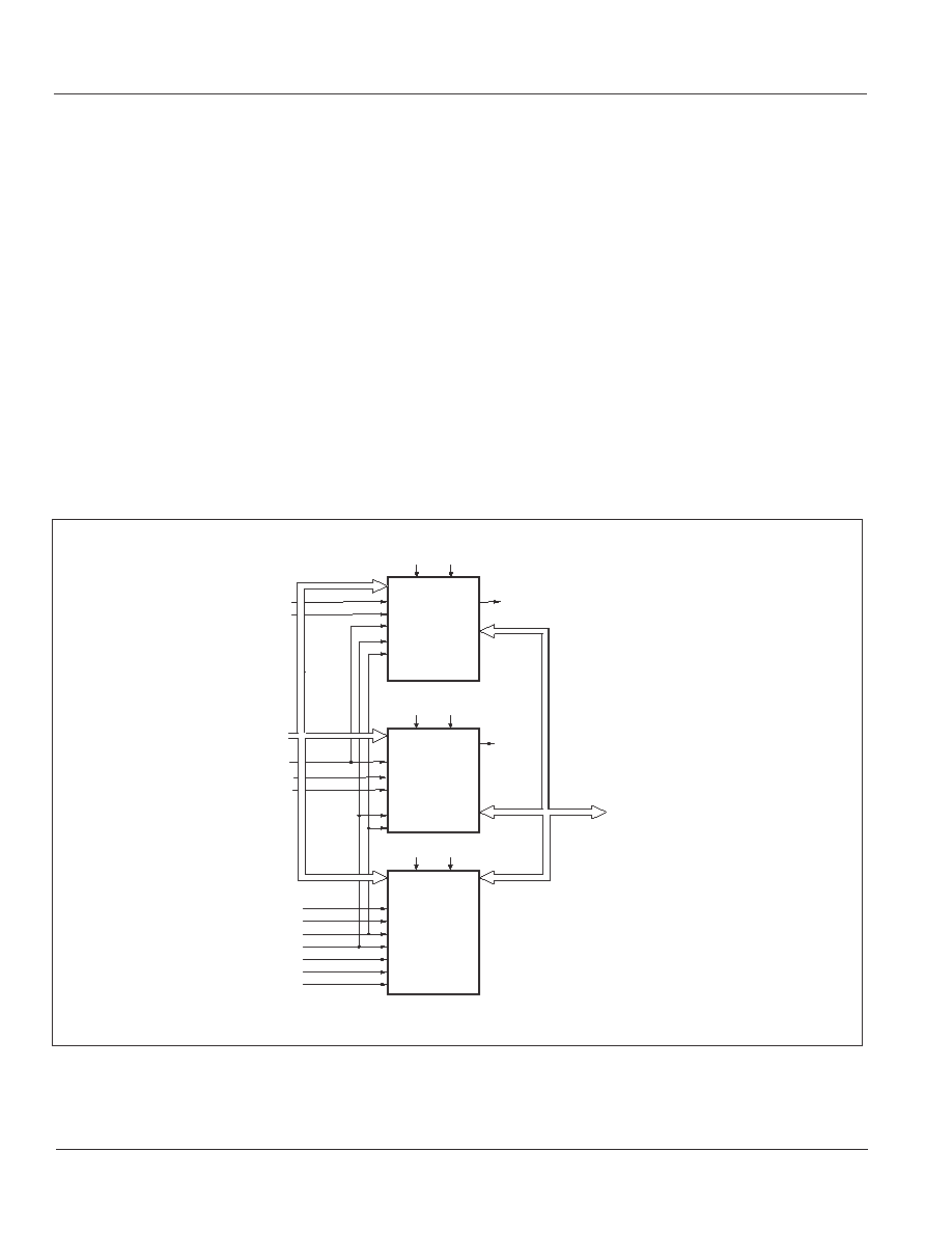
GENERAL DESCRIPTION
This 107-ball MCP is a space-saving combination of 3 memories: 64Mbit Flash, 32Mbit Flash, and 32Mbit Pseudo
SRAM. The 64Mbit FLASH (FLASH 1) contains 4,194,304 words, the 32Mbit FLASH (FLASH 2) contains 2,097,152
words, and the 32Mbit PSRAM contains 2,097,152 words. Each word is 16 bits wide. Data lines DQ0-DQ15 handle
the access for all three memories. Write Enable, Output Enable, and A0-A20 are shared among the three
memories. Single Byte data on the PSRAM can be accessed one at a time on DQ0-DQ7 or DQ8-DQ15 by using
LB
or
UB
, respectively.
The package uses a 3.0V power supply for all operations. No other source is required for program and erase operations.
The FLASH can be programmed in system using this 3.0V supply, or can be programmed in a standard EPROM
programmer.
The FLASH chips are compatible with the JEDEC FLASH command set standard. The FLASH access time is 70ns and
the PSRAM access time is 65ns.
Each FLASH memory implements an architecture composed of two virtual banks that allows simultaneous operation on
each bank. Optimized performance can be achieved by first initializing a program or erase function in one bank, then
immediately starting a read from the other bank. Both operations would then be operating simultaneously on the same
chip, with zero latency.
MCP BLOCK DIAGRAM
GND
GND
V
CCf2
RY/
BY
2
32-MBIT
PSRAM
32-MBIT
Flash Memory
DQ0-DQ15
LB
UB
WE
OE
CE1
r
CE2r
A0-A20
V
CCr
PE
(Flash 2)
A0-A21
CE
f
2
RESET
2
WP
/ACC
64-MBIT
Flash Memory
(Flash 1)
A0-A21
RESET
1
CE
f
1
GND
V
CCf1
RY/
BY
1
A0-A21
Integrated Silicon Solution, Inc. -- www.issi.com --
1-800-379-4774
3
PRELIMINARY INFORMATION
Rev. 00D
03/24/03
IS75V16F96GS32
ISSI
Æ
PIN DESCRIPTIONS
A0-A20
Address Inputs, Common
A21
Address Input, FLASH 1
DQ0-DQ15
Data Inputs/Outputs, Common
RESET
1
Reset, FLASH 1
RESET
2
Reset, FLASH 2
CE1
r, CE2r
Chip Enable, PSRAM
CE
f1
Chip Enable, FLASH
CE
f2
Chip Enable, FLASH 2
OE
Output Enable, Common
WE
Write Enable, Common
PE
Partial Enable, PSRAM
LB
Lower-byte Control, PSRAM
UB
Upper-byte Control, PSRAM
WP
/ACC
Write Protect/Acceleration Pin, Both Flash
RY/
BY1
Ready/Busy Output , FLASH 1
RY/
BY2
Ready/Busy Output , FLASH 2
NC
No Connection
DU
Do Not Use
Vccf1
Power, FLASH 1
Vccf2
Power, FLASH 2
Vccr
Power, PSRAM
GND
Ground, Common
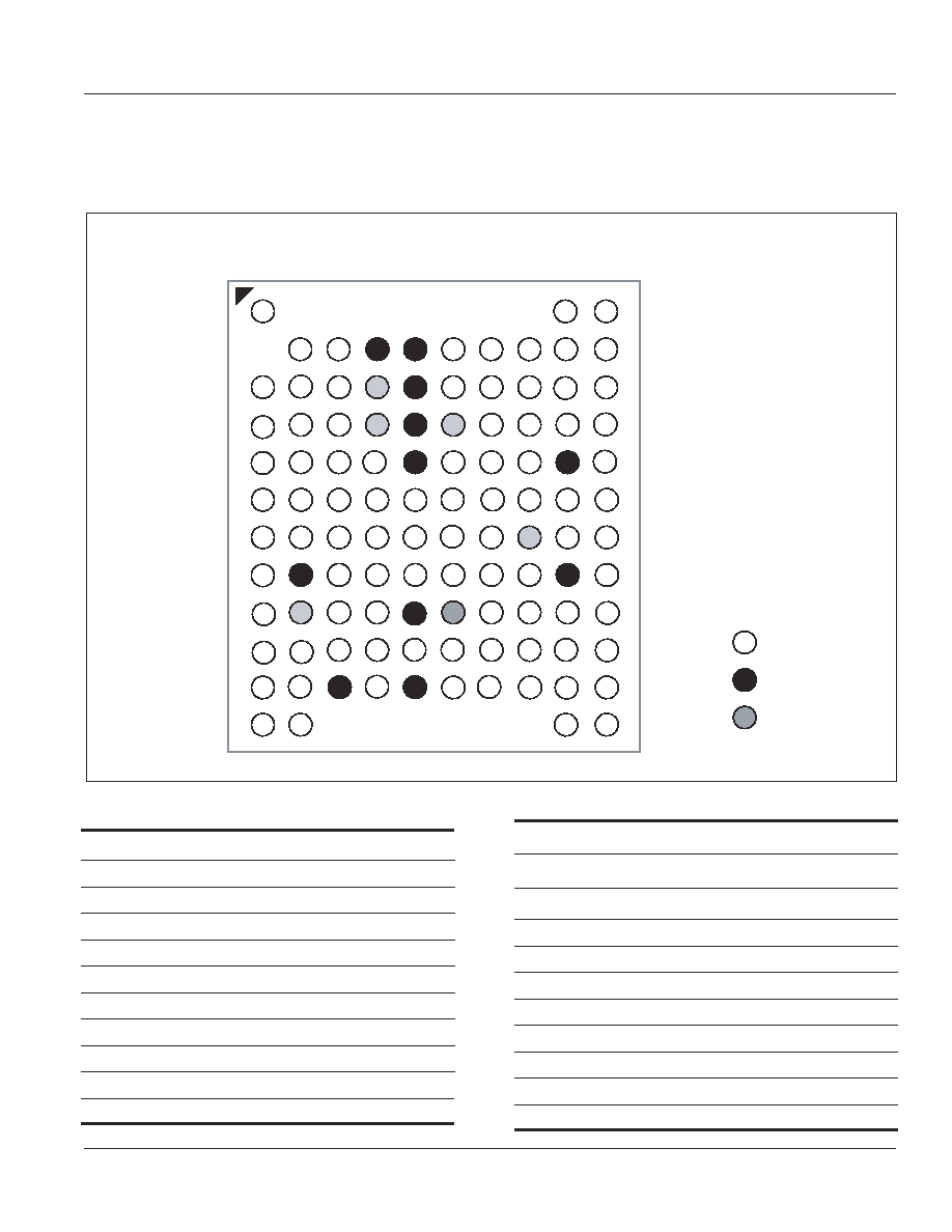
PIN CONFIGURATION (96 Mb FLASH and 32 Mb PSRAM)
PACKAGE CODE: B 107 BALL FBGA (Top View) (9.00 mm x 10.00 mm Body, 0.8 mm Ball Pitch)
1 2 3 4 5 6 7 8 9 10
A
B
C
D
E
F
G
H
J
K
L
M
NC
NC
NC
NC
NC
NC
NC
A3
A2
A1
A0
CEf1
CE1r
A7
A6
A5
A4
GND
OE
DQ0
DQ8
LB
UB
A18
A17
DQ1
DQ9
DQ10
DQ2
CE
f2
WP/
ACC
RESET
1
RY/
BY
1
DQ3
Vccf1
DQ11
Vccf2
NC
WE
CE2r
A20
DQ4
Vccr
NC
NC
A8
A19
A9
A10
DQ6
DQ13
DQ12
DQ5
A11
A12
A13
A14
PE
DQ15
DQ7
DQ14
A15
A21
NC
A16
Vccf1
GND
NC
NC
NC
NC
NC
NC
Shared
Flash Only
PSRAM Only
NC
NC
NC
NC
NC
NC
NC
NC
NC
NC
NC
NC
NC
NC
NC
NC
NC
NC
NC
NC
NC
NC
NC
NC
NC
DU
DU
DU
DU
GND
RESET
2
RY/
BY
2
GND

4
Integrated Silicon Solution, Inc. -- www.issi.com --
1-800-379-4774
PRELIMINARY INFORMATION
Rev. 00D
03/24/03
IS75V16F96GS32
ISSI
Æ
OPERATION
(1,2)
C
C
C
C
CE
E
E
E
E
f1
C
C
C
C
CE
E
E
E
E
f2
C
C
C
C
CE
E
E
E
E1
11
1
1
r CE2r
OE
OE
OE
OE
OE W
W
W
W
WE
E
E
E
E L
LL
L
LB
B
B
B
B
s
U
U
U
U
UB
B
B
B
B
s
P
P
P
P
PE
E
E
E
E
A
21
-A
0
DQ
7
-DQ
0
DQ
15
-DQ
8
RESET1
RESET1
RESET1
RESET1
RESET1 RESET2
RESET2
RESET2
RESET2
RESET2 WP
WP
WP
WP
WP
/ACC
(12)
Full Standby
H
H
H
H
X
X
X
X
H
X
High-Z
High-Z
H
H
X
Output Disable
(3)
H
H
L
H
H
H
X
X
H
X
(10)
High-Z
High-Z
H
H
X
L
H
H
H
H
H
X
X
H
X
High-Z
High-Z
H
H
X
H
L
H
H
H
H
X
X
H
X
High-Z
High-Z
H
H
X
Read from FLASH 1
(4)
L
H
H
H
L
H
X
X
H
Valid
D
OUT
D
OUT
H
H
X
Read from FLASH 2
(4)
H
L
H
H
L
H
X
X
H
Valid
D
OUT
D
OUT
H
H
X
Write to FLASH 1
L
H
H
H
H
L
X
X
H
Valid
D
IN
D
IN
H
H
X
Write to FLASH 2
H
L
H
H
H
L
X
X
H
Valid
D
IN
D
IN
H
H
X
Read from PSRAM
(5)
H
H
L
H
L
H
L
(9)
L
(9)
H
Valid
D
OUT
D
OUT
H
H
X
Write to PSRAM
H
H
L
H
H
L
L
L
H
Valid
D
IN
D
IN
H
H
X
H
H
L
H
H
L
H
L
H
Valid
High-Z
D
IN
H
H
X
H
H
L
H
H
L
L
H
H
Valid
D
IN
High-Z
H
H
X
FLASH 1Temporary
Sector Group
X
X
X
X
X
X
X
X
X
X
X
X
V
ID
X
X
Unprotection
(6)
FLASH 2 Temporary
Sector Group
X
X
X
X
X
X
X
X
X
X
X
X
X
V
ID
X
Unprotection
(6)
FLASH 1
Hardware Reset
X
X
H
H
X
X
X
X
X
X
High-Z High-Z
L
X
X
FLASH 2
Hardware Reset
X
X
H
H
X
X
X
X
X
X
High-Z
High-Z
X
L
X
Boot Block Sector
Write Protection
X
X
X
X
X
X
X
X
X
X
X
X
X
X
L
PSRAM Power
Down Program
(7)
H
H
H
H
X
X
X
X
L
Valid
High-Z
High-Z
H
H
X
PSRAM No Read
H
H
L
H
L
H
H
H
H
Valid
High-Z
High-Z
H
H
X
PSRAM
Power Down
(8)
X
X
X
L
X
X
X
X
X
X
X
X
X
X
X
Legend : L = VIL, H = VIH, X = VIL or VIH. See "DC CHARACTERISTICS" for voltage levels.
Notes:
1. Other operations except for indicated this column are prohibited.
2. Do not apply
CE
f = VIL,
CE
1r = VIL and CE2r = VIH all at once.
3. PSRAM Output Disable condition should not be kept longer than 1ms.
4.
WE
can be VIL if
OE
is VIL,
OE
at VIH initiates the write operations.
5. PSRAM
LB
,
UB
control at Read operation is not supported.
6. It is also used for the extended sector group protections.
7. The PSRAM Power Down Program can be performed one time after compliance of Power-UP timings and it should not be re-
programmed after regular Read or Write.
8. PSRAM Power Down mode can be entered from Standby state and all DQ pins are in High-Z state. IPDr current and data retention
depends on the selection of Power Down Program.
9. Either or both
LB
and
UB
must be Low for PSRAM Read Operation.
10. Can be either VIL or VIH but must be valid before Read or Write.
11. See " PSRAM Power Down Program Key Table " located in the next page.
12. Protect " outer most " 2x8K bytes ( 4 words ) on both ends of the boot block sectors.
DEVICE BUS OPERATION

Integrated Silicon Solution, Inc. -- www.issi.com --
1-800-379-4774
5
PRELIMINARY INFORMATION
Rev. 00D
03/24/03
IS75V16F96GS32
ISSI
Æ
ABSOLUTE MAXIMUM RATINGS
(1,5)
Rating
Symbol
Parameter
Min.
Max.
Unit
Tstg
Storage Temperature
≠55
+125
∞C
T
A
Ambient Temperature with Power Applied
≠30
+85
∞C
V
IN
,V
OUT
Voltage with Respect to Ground All Pins
(2)
≠0.3
V
CC
+ 0.3
(6)
V
V
CC
f1,V
CC
f2
V
CC
f Supply
(2)
≠0.3
3.5
V
V
CC
r
V
CC
r Supply
(2)
≠0.3
3.5
V
V
IN
RESET1
,
RESET2
(3)
-0.5
+13.0
V
V
ACC
WP
/ACC
(4)
≠0.5
+10.5
V
Notes:
1. Voltage is defined on the basis of GND = 0 V.
2. Minimum DC voltage on input or I/O pins is -0.3 V. During voltage transitions, input or I/O pins may undershoot
GND to -1.0 V for periods of up to 20 ns. Maximum DC voltage on input or I/O pins is V
CC
f1+ 0.3V , V
CC
f2+ 0.3V
or VCCr + 0.3 V. During voltage transitions, input or I/O pins may overshoot to V
CC
f1+ 2.0V , V
CC
f2+ 2.0 V or VCCr + 1.0 V
for periods of up to 20 ns.
3. Minimum DC input voltage on
RESET1
or
RESET2
pin is -0.5 V. During voltage transitions,
RESET1
or
RESET2
pin may
undershoot GND to -2.0 V for periods of up to 20 ns.
Voltage difference between input and supply voltage (VIN-V
CC
f1 or V
CC
f2) does not exceed 9.0 V.
Maximum DC input voltage on each
RESET
pin is +13.0 V, and it may overshoot to +14.0 V for periods of up to 20 ns.
4. Minimum DC input voltage on
WP
/ACC pin is -0.5 V. During voltage transitions,
WP
/ACC pin may undershoot
GND to -2.0 V for periods of up to 20 ns. Maximum DC input voltage on
WP
/ACC pin is +10.5 V which may
overshoot to +12.0 V for periods of up to 20 ns, when V
CC
f1 or V
CC
f2 is applied.
5. Stress greater than those listed under ABSOLUTE MAXIMUM RATINGS may cause permanent damage to the device. This is a
stress rating only and functional operation of the device at these or any other conditions above those indicated in the operational
sections of this specification is not implied. Exposure to absolute maximum rating conditions for extended periods may affect
reliability.
6. This Vcc refers to the minimum of V
CC
f1, V
CC
f2, or Vccr .
RECOMMENDED OPERATING CONDITIONS
Rating
Symbol
Parameter
Min.
Max.
Unit
T
A
Ambient Temperature
≠30
+85
∞C
V
CC
f1,V
CC
f2
V
CC
f Supply Voltages
2.7
3.3
V
V
CC
r
V
CC
r Supply Voltages
2.7
3.3
V
Note:
Voltage is defined on the basis of GND = 0 V.