IS80C51
IS80C31
Integrated Silicon Solution, Inc. -- 1-800-379-4774
1
MC003-1D
11/19/98
ISSI
Æ
ISSI reserves the right to make changes to its products at any time without notice in order to improve design and supply the best possible product. We assume no responsibility for any errors which
may appear in this publication. © Copyright 1998, Integrated Silicon Solution, Inc.
IS80C51
IS80C31
CMOS SINGLE CHIP
8-BIT MICROCONTROLLER
NOVEMBER 1998
FEATURES
∑ 80C51 based architecture
∑ 4K x 8 ROM (IS80C51 only)
∑ 128 x 8 RAM
∑ Two 16-bit Timer/Counters
∑ Full duplex serial channel
∑ Boolean processor
∑ Four 8-bit I/O ports, 32 I/O lines
∑ Memory addressing capability
≠ 64K ROM and 64K RAM
∑ Power save modes:
≠ Idle and power-down
∑ Six interrupt sources
∑ Most instructions execute in 0.3
µ
s
∑ CMOS and TTL compatible
∑ Maximum speed: 40 MHz @ Vcc = 5V
∑ Industrial temperature available
∑ Packages available:
≠ 40-pin DIP
≠ 44-pin PLCC
≠ 44-pin PQFP
GENERAL DESCRIPTION
The
ISSI
IS80C51 and IS80C31 are high-performance
microcontrollers fabricated using high-density CMOS
technology. The CMOS IS80C51/31 is functionally
compatible with the industry standard 80C51
microcontrollers.
The IS80C51/31 is designed with 4K x 8 ROM (IS80C51
only); 128 x 8 RAM; 32 programmable I/O lines; a serial
I/O port for either multiprocessor communications, I/O
expansion or full duplex UART; two 16-bit timer/counters;
a six-source, two-priority-level, nested interrupt structure;
and an on-chip oscillator and clock circuit. The
IS80C51/31 can be expanded using standard TTL
compatible memory.
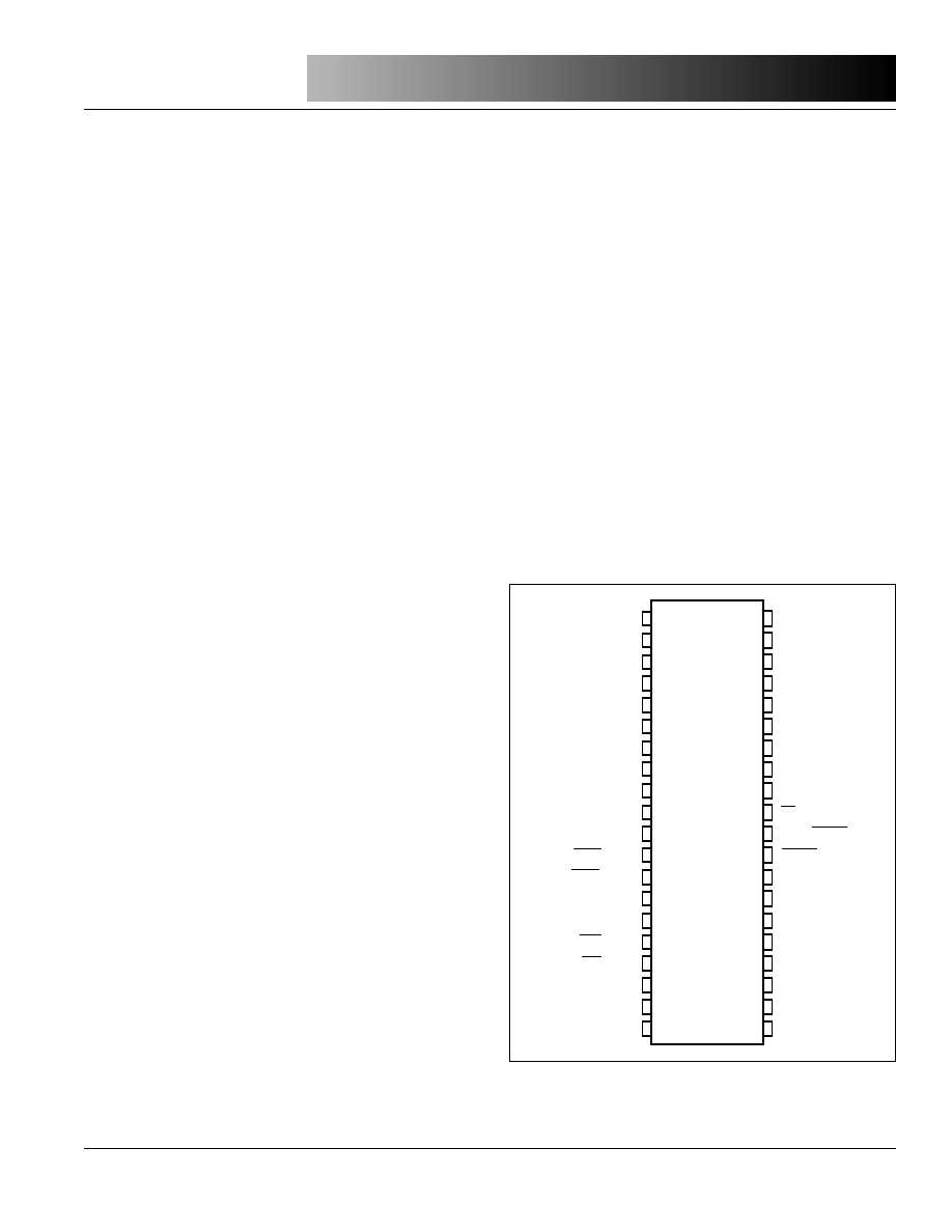
Figure 1. IS80C51/31 Pin Configuration: 40-pin PDIP
1
2
3
4
5
6
7
8
9
10
11
12
13
14
15
16
17
18
19
20
40
39
38
37
36
35
34
33
32
31
30
29
28
27
26
25
24
23
22
21
P1.0
P1.1
P1.2
P1.3
P1.4
P1.5
P1.6
P1.7
RST
RxD/P3.0
TxD/P3.1
INT0/P3.2
INT1/P3.3
T0/P3.4
T1/P3.5
WR/P3.6
RD/P3.7
XTAL2
XTAL1
GND
VCC
P0.0/AD0
P0.1/AD1
P0.2/AD2
P0.3/AD3
P0.4/AD4
P0.5/AD5
P0.6/AD6
P0.7/AD7
EA/VPP
ALE/PROG
PSEN
P2.7/A15
P2.6/A14
P2.5/A13
P2.4/A12
P2.3/A11
P2.2/A10
P2.1/A9
P2.0/A8
ISSI
Æ
IS80C51
IS80C31
2
Integrated Silicon Solution, Inc. -- 1-800-379-4774
MC003-1D
11/19/98
ISSI
Æ
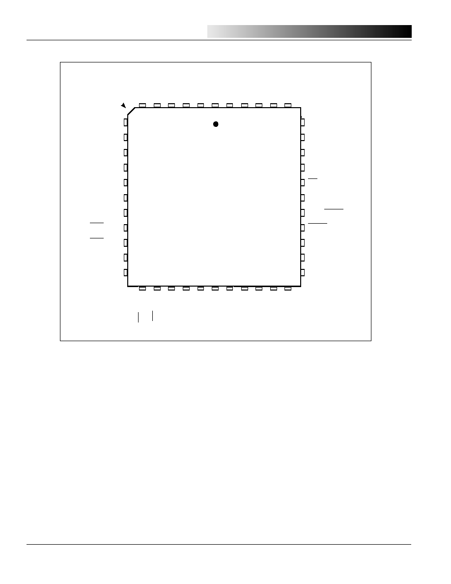
WR/P3.6
RD/P3.7
XTAL2
XTAL1
GND
NC
A8/P2.0
A9/P2.1
A10/P2.2
A11/P2.3
A12/P2.4
P1.4
P1.3
P1.2
P1.1
P1.0
NC
VCC
P0.0/AD0
P0.1/AD1
P0.2/AD2
P0.3/AD3
P0.4/AD4
P0.5/AD5
P0.6/AD6
P0.7/AD7
EA/VPP
NC
ALE/PROG
PSEN
P2.7/A15
P2.6/A14
P2.5/A13
P1.5
P1.6
P1.7
RST
RxD/P3.0
NC
TxD/P3.1
INT0/P3.2
INT1/P3.3
T0/P3.4
T1/P3.5
7
8
9
10
11
12
13
14
15
16
17
39
38
37
36
35
34
33
32
31
30
29
INDEX
4
3
6
5
2
1
44
18
19
20
21
22
23
24
43
42
41
40
25
26
27
28
TOP VIEW
Figure 2. IS80C51/31 Pin Configuration: 44-pin PLCC
IS80C51
IS80C31
Integrated Silicon Solution, Inc. -- 1-800-379-4774
3
MC003-1D
11/19/98
ISSI
Æ
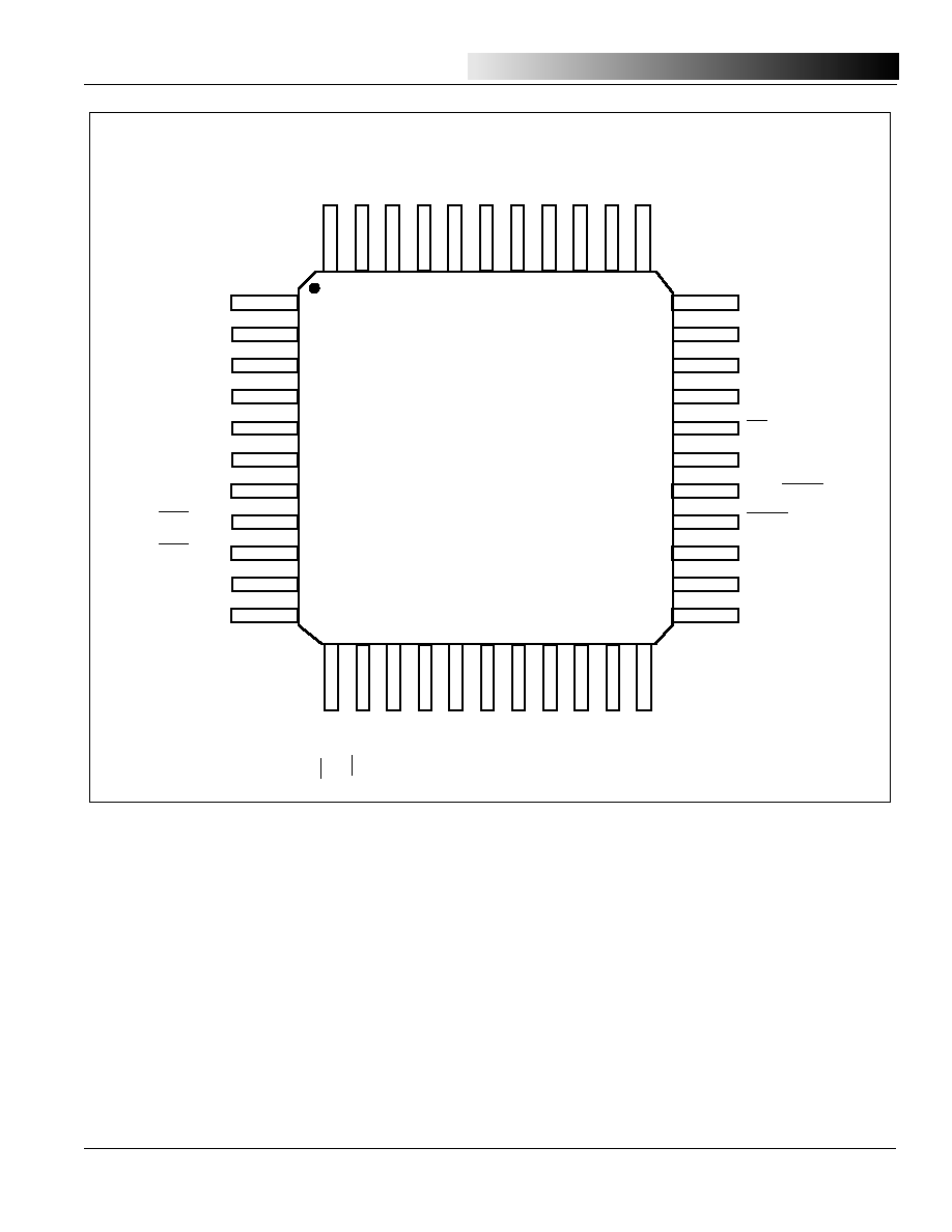
Figure 3. IS80C51/31 Pin Configuration: 44-pin PQFP
WR/P3.6
RD/P3.7
XTAL2
XTAL1
GND
NC
A8/P2.0
A9/P2.1
A10/P2.2
A11/P2.3
A12/P2.4
P1.4
P1.3
P1.2
P1.1
P1.0
NC
VCC
P0.0/AD0
P0.1/AD1
P0.2/AD2
P0.3/AD3
P0.4/AD4
P0.5/AD5
P0.6/AD6
P0.7/AD7
EA/VPP
NC
ALE/PROG
PSEN
P2.7/A15
P2.6/A14
P2.5/A13
P1.5
P1.6
P1.7
RST
RxD/P3.0
NC
TxD/P3.1
INT0/P3.2
INT1/P3.3
T0/P3.4
T1/P3.5
1
2
3
4
5
6
7
8
9
10
11
33
32
31
30
29
28
27
26
25
24
23
42
41
44
43
40
39
38
12
13
14
15
16
17
18
37
36
35
34
19
20
21
22
IS80C51
IS80C31
4
Integrated Silicon Solution, Inc. -- 1-800-379-4774
MC003-1D
11/19/98
ISSI
Æ
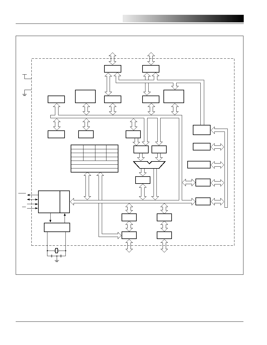
Figure 4. IS80C51/31 Block Diagram
PCON
SCON
TMOD TCON
TH0
TL0
TH1
TL1
SBUF
IE
IP
INTERRUPT BLOCK
SERIAL PORT BLOCK
TIMER BLOCK
P3
DRIVERS
P3
LATCH
PSW
TIMING
AND
CONTROL
OSCILLATOR
XTAL2
XTAL1
INSTRUCTION
REGISTER
P3.0-P3.7
P1
DRIVERS
P1
LATCH
DPTR
BUFFER
PC
INCREMENTER
PROGRAM
COUNTER
PROGRAM
ADDRESS
REGISTER
P1.0-P1.7
P2.0-P2.7
P0.0-P0.7
PSEN
ALE
RST
EA
TMP2
ALU
ACC
STACK
POINT
B
REGISTER
VCC
RAM ADDR
REGISTER
P2
LATCH
P0
LATCH
P2
DRIVERS
P0
DRIVERS
ADDRESS
DECODER
& 128
BYTES RAM
ADDRESS
DECODER
&
4K ROM
TMP1

IS80C51
IS80C31
Integrated Silicon Solution, Inc. -- 1-800-379-4774
5
MC003-1D
11/19/98
ISSI
Æ
Table 1. Detailed Pin Description
Symbol
PDIP
PLCC
PQFP
I/O
Name and Function
ALE
30
33
27
I/O
Address Latch Enable: Output pulse for latching the low byte
of the address during an address to the external memory. In
normal operation, ALE is emitted at a constant rate of 1/6 the
oscillator frequency, and can be used for external timing or
clocking. Note that one ALE pulse is skipped during each
access to external data memory.
EA
31
35
29
I
External Access enable:
EA
must be externally held low to
enable the device to fetch code from external program memory
locations 0000H to FFFFH. If
EA
is held high, the device
executes from internal program memory unless the program
counter contains an address greater than 0FFFH.
P0.0-P0.7
39-32
43-36
37-30
I/O
Port 0: Port 0 is an 8-bit open-drain, bidirectional I/O port. Port
0 pins that have 1s written to them float and can be used as high-
impedance inputs. Port 0 is also the multiplexed low-order
address and data bus during accesses to external program and
data memory. In this application, it uses strong internal pullups
when emitting 1s.
P1.0-P1.7
1-8
2-9
40-44
I/O
Port 1: Port 1 is an 8-bit bidirectional I/O port with internal
1-3
pullups. Port 1 pins that have 1s written to them are pulled high
by the internal pullups and can be used as inputs. As inputs,
Port 1 pins that are externally pulled low will source current
because of the internal pullups. (See DC Characteristics: I
IL
).
The Port 1 output buffers can sink/source four TTL inputs.
Port 1 also receives the low-order address byte during ROM
verification.
P2.0-P2.7
21-28
24-31
18-25
I/O
Port 2: Port 2 is an 8-bit bidirectional I/O port with internal
pullups. Port 2 pins that have 1s written to them are pulled high
by the internal pullups and can be used as inputs. As inputs,
Port 2 pins that are externally pulled low will source current
because of the internal pullups. (See DC Characteristics: I
IL
).
Port 2 emits the high order address byte during fetches from
external program memory and during accesses to external data
memory that used 16-bit addresses (MOVX @ DPTR). In this
application, Port 2 uses strong internal pullups when emitting
1s. During accesses to external data memory that use 8-bit
addresses (MOVX @ Ri [i = 0, 1]), Port 2 emits the contents of
the P2 Special Function Register.
Port 2 also receives the high-order bits and some control
signals during ROM verification.