
IS82C600
Integrated Silicon Solution, Inc. -- 1-800-379-4774
1
PRELIMINARY
TB001-0B
01/20/99
ISSI
Æ
This document contains PRELIMINARY DATA. ISSI reserves the right to make changes to its products at any time without notice in order to improve design and supply the best possible product.
We assume no responsibility for any errors which may appear in this publication. © Copyright 1999, Integrated Silicon Solution, Inc.
TRAILBLAZER
High-Speed SRAM with
Address Decoding and Ready Logic
FEATURES
∑ Zero wait-state performance on the Primary
Bus
-- Point-to-point interface between the SRAM
and the high-speed processor
∑ Seamless interface to Texas Instruments'
TMS320LC54x high-speed processor
∑ Integrates the single-ported SRAM with a dual-
ported interface
and handshake
-- 9 ns access time to the SRAM
-- Can also be used as a standalone, high-
speed SRAM
∑ Integrates the port-to-port bridge function
-- Broadcasts all processor cycles from
Primary Bus to the Secondary Bus
-- Programmability to only broadcast
non-SRAM cycles to the Secondary Bus
-- Supports older, slower peripheral devices on
the Secondary Bus
-- Allows the processor transparent access to
the devices on the Secondary Bus through
XCVR
pin
-- Supports a Boot ROM on the Secondary Bus
GENERAL DESCRIPTION
The IS82C600 TrailBlazer simplifies high-speed system
design and layout, providing an SRAM with zero wait-state
performance up to 90 MHz, address coding, and "Ready"
logic. In many cases, TrailBlazer allows existing system
designs to be easily upgraded, enabling the re-use of
already available ASICs and glue logic.
A key benefit of the TrailBlazer device is its ability to relieve
high-performance processors from a necessity to drive
heavily loaded multidrop buses by providing a point-to-
∑ Features Address Decoding and Ready Logic
-- A total of six Chip Selects
-- Supports "Ready" logic signal generation for
memory and I/O
-- Eliminates PALs for address decoding and
ready logic
-- No "glue logic" interface for local peripherals
on the Secondary Bus processor
∑ Allows dynamic re-allocation of memory spaces
for transparent block moves
-- Programmable memory decoding allows
memory blocks to be accessed as either
Program Space (
PS
) or Data Space (
DS
)
-- Programmable registers to map the internal
SRAM memory and external secondary port
devices into Data Space (
DS
), Program
Space (
PS
) and I/O Space (
IS
)
∑ Can also be used as a standalone, high-speed
SRAM
∑ Allows the shadowing of the ROM on the
Secondary Bus into the on-board SRAM
IS82C600
point, low-load interconnect to the high-speed memory
and buffering of the slower speed devices. This could allow
the processors to operate at a maximum frequency with
zero wait-states. Also, it eases PCB timing and layout-
related considerations, often allowing a reduction in the
number of PC board layers and the lowering of noise.
Programmable decodes and "Ready" generation logic
built into the TrailBlazer eliminates the need for expensive
PALs, other glue logic, and additional board space.
PRELIMINARY
JANUARY 1999
ISSI
Æ
2
Integrated Silicon Solution, Inc. -- 1-800-379-4774
PRELIMINARY
TB001-0B
01/20/99
IS82C600
ISSI
Æ
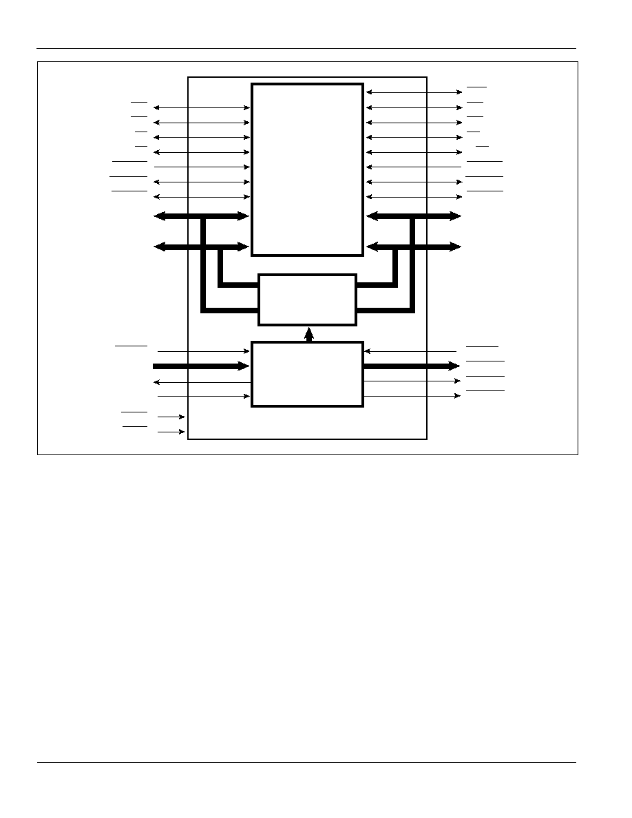
Figure 1. TrailBlazer Functional Block Diagram
PRODUCT OVERVIEW
The IS82C600 TrailBlazer integrates a high-speed 64K x
16 SRAM with a processor port-to-processor port bridge
function. This simplifies any high-speed designs by
providing a fast access time for the processor on the
Primary Port and enabling for a low-cost implementation of
a high-frequency system.
TrailBlazer combines a high-performance memory array,
programmable decodes, and "Ready" logic to achieve
maximum performance and flexibility, while keeping costs
at a minimum. In order to simplify system development,
TrailBlazer duplicates the Primary Bus signals on its
Secondary Bus to permit the use of existing system
components
and ASICs together with a new generation of
high-performance processors.
On its Primary Bus, the TrailBlazer provides a high-speed
SRAM interface and then broadcasts the Primary Bus
cycles to its Secondary Bus, allowing the processor on its
Primary Bus to access peripherals on its Secondary Bus.
In many cases, since the peripherals are accessed by the
same signals, existing ASICs can be re-used.
TrailBlazer provides an optimized, seamless interface to
TI TMS320LC54x high-speed processor without the need
for any glue logic interfaces for local peripherals on the
Secondary Bus. TrailBlazer can also be used as shared
Local or Global Memory for a dual processor-based system
where the Chip Select logic on each bus allows for the
same data to be accessed at different locations in memory,
if so desired.
DECODER
SRAM
64K x 16
BUS
REPEATER
PSp
DSp
ISp
R/Wp
HOLDAp
IOSTRBp
MSTRBp
Dp[15:0]
Ap[15:0]
Ds[15:0]
As[15:0]
CSINTp
Ap[21:16]
RDY
CLK
PRGM
XCVR
CSINTs
CSMEMs[5:0]
WEMEMs
OEMEMs
PSs
DSs
ISs
R/Ws
HOLDAs
IOSTRBs
MSTRBs
PSp
DSp
ISp
R/Wp
HOLDAp
IOSTRBp
MSTRBp
WEs
PSs
DSs
ISs
R/Ws
HOLDAs
IOSTRBs
MSTRBs
IS82C600
Integrated Silicon Solution, Inc. -- 1-800-379-4774
3
PRELIMINARY
TB001-0B
01/20/99
ISSI
Æ
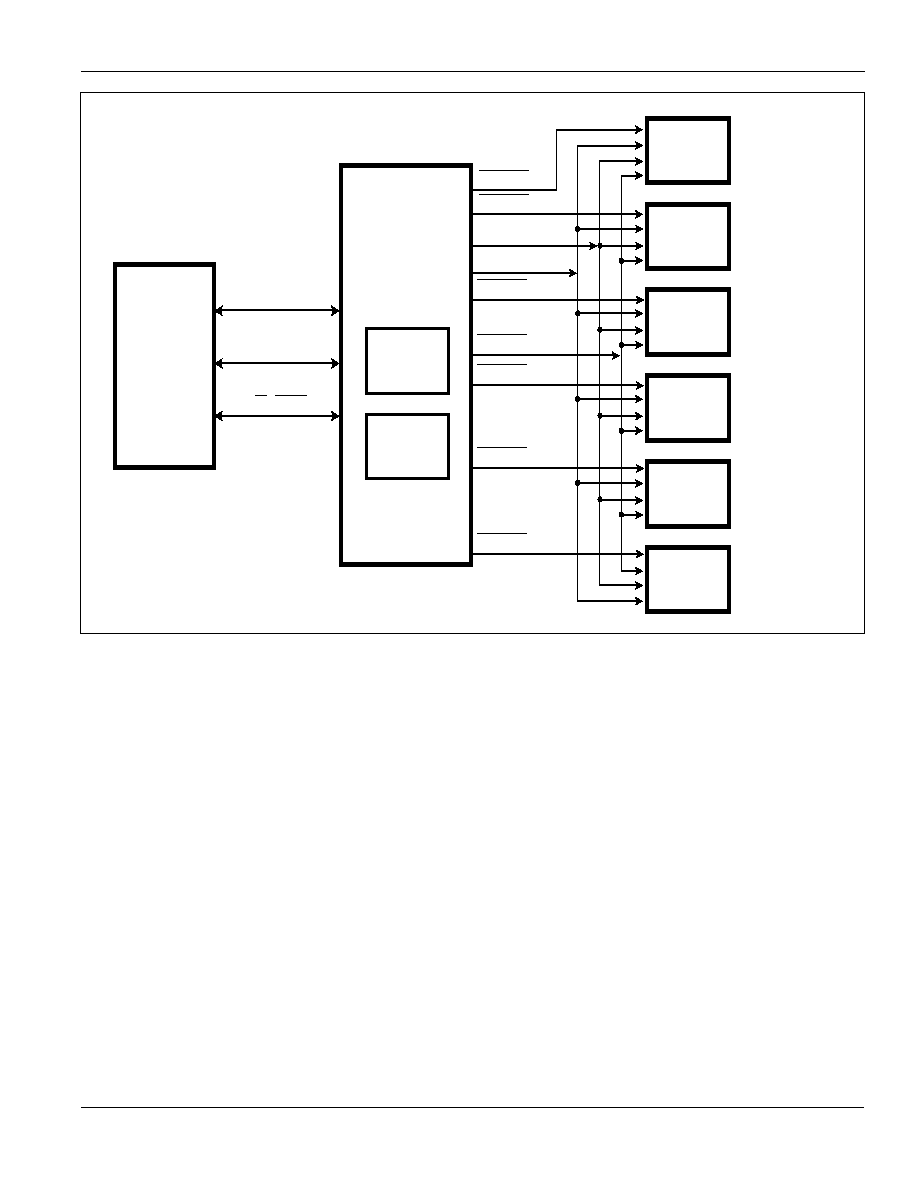
Figure 2. TrailBlazer System Block Diagram with High-Speed DSP on the Primary Bus and
the Slower Existing DSP System Components on the Secondary Bus
DSP
CSMEMs[0]
TRAILBLAZER
IS82C600
LOCAL
DEVICE 1
LOCAL
DEVICE 2
32K x 16
32K x 16
(REGISTER 0)
(DEFAULT)
(REGISTER 5)
(REGISTER 4)
(REGISTER 3)
(REGISTER 2)
(REGISTER 1)
LOCAL
DEVICE 3
LOCAL
DEVICE 4
LOCAL
DEVICE 5
LOCAL
DEVICE 6
CSMEMs[1]
As[15:0]
Ap[21:0]
Dp[15:0]
R/W, STRB
Ds[15:0]
CSMEMs[2]
CSMEMs[3]
CSMEMs[4]
CSMEMs[5]
WEMEMs

4
Integrated Silicon Solution, Inc. -- 1-800-379-4774
PRELIMINARY
TB001-0B
01/20/99
IS82C600
ISSI
Æ
PIN INFORMATION
Complete pin information on the device is organized as
follows:
∑ Overview
∑ Conventions
∑ Pin Diagram
∑ Pin Assignment Table--Arranged by Pin Number
∑ Pin Assignment Table--Arranged by Ball Location
∑ Detailed Pin Descriptions
Overview
The R/
W
signal determines the direction of the bus
transaction.
Some processors, including TI TMS320LC54X, have three
major memory spaces. Program Space (
PS
); Data Space
(
DS
); and I/O Space (
IS
). The Memory Space signals (
DS
,
PS
, and
IS
) select the memory address space being
accessed (Data, Program, or I/O). No more than one of the
Memory Space signals can be asserted at the same time.
Data or Program spaces (or any part of these spaces) can
be mapped into either internal SRAM of the TrailBlazer or
any external devices. I/O space can only be mapped to
external devices. The TrailBlazer's internal SRAM has two
32KB regions that are restricted to either
DS
or
PS
space.
Register 0 controls the decoding for the internal SRAM.
Registers 1 through 5 control the address decoding for the
external devices on the Secondary Bus. For processors
that have A15 as the MSB, the three memory
spaces are restricted to 64KB each. However, the registers
do allow for programmable address ranges in 8KB blocks.
For processors with A[21:16] as the MSB, there is a 4MB
maximum address space that can be partitioned by
programming Registers 1 to 5.
Chip Selects (
CSMEM
x) are used to select external devices
on the Secondary Bus. These signals are generated by
combinations of the Memory Space signals and Addresses
Ap[13:21].
Strobes (
MSTRB
and
IOSTRB
) validate Memory Space
selections.
PS
and
DS
have to be validated by the assertion
of
MSTRB
and
IS
has to be validated by the assertion of
IOSTRB
.
The following provides detailed technical information
related to the pins on the device. For ease of reference, the
pin information is presented in a table format arranged both
by pin numbers and by pin names. A pin diagram has also
been included to be used as a visual point of reference.
Conventions
Table 1 details conventions that are used to present
information on the pins.
Table 1. Pin Conventions
Convention
Meaning
NC
This pin is reserved for ISSI, Inc. and must
be left as a 'No Connect'
I
Input-only
O
Output-only
I/O
Input or Output (Bi-directional)
Power
Power pin
Ground
Ground pin
SIGNAL
Active (or asserted) state occurs when pin
is at a low voltage
/
Multiplexed or Dual functionality
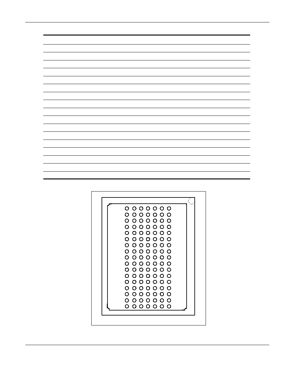
Pin Diagram
Refer to Figure 3 and Table 2 for the pin diagram for the
TrailBlazer device. It depicts the pin names and the
corresponding ball location. Pins marked as 'NC' are not
available and are defined as 'No Connect' pins. For more
detailed information on the pins refer to Table 5.
IS82C600
Integrated Silicon Solution, Inc. -- 1-800-379-4774
5
PRELIMINARY
TB001-0B
01/20/99
ISSI
Æ
Figure 3. TrailBlazer Pin Diagram
7
6
5
4
BOTTOM VIEW
3
2
1
A
B
C
D
E
F
G
H
J
K
L
M
N
P
R
T
U
Table 2. Pin Configuration: 119-pin PBGA
1
2
3
4
5
6
7
A
Ap18
Ap16
Ap4
Ap5
Ap11
XCVR
ISp
B
Ap19
Ap17
Ap3
Ap6
Ap12
PSp
DSp
C
Ap21
Ap20
Ap2
Ap7
Ap13
Dp0
Dp1
D
Ds1
Ds0
Ap1
Ap8
Ap14
Dp2
Dp3
E
Ds3
Ds2
Ap0
Ap9
Ap15
Dp4
Dp5
F
Ds4
GND
GND
Q
Ap10
GND
Q
V
CC
Dp6
G
Ds7
Ds6
Ds5
Dp7
HOLDAp
CSINTp
R/
W
p
H
CLK
GND
Q
RDY
V
CCQ
RDp
GND
Q
IOSTRBp
J
Ds8
OEMEMs
V
CCQ
V
CCQ
WEs
WEp
MSTRBp
K
Ds9
GND
Q
WEMEMs
V
CCQ
IOSTRBs
GND
Q
MSTRBs
L
Ds10
Ds11
As1
As7
CSINTs
R/
W
s
RDs
M
Ds12
Vcc
GND
Q
As8
GND
Q
GND
HOLDAs
N
Ds13
Ds14
As2
As9
Dp10
Dp9
Dp8
P
Ds15
CSMEMs0
As3
As10
Dp13
Dp12
Dp11
R
CSMEMs1
CSMEMs2
As4
As11
PRGM
DSs
Dp14
T
CSMEMs3
CSMEMs5
As5
As12
As15
ISs
Dp15
U
CSMEMs4
As0
As6
As13
As14
PSs
NC