Integrated Silicon Solution, Inc. -- www.issi.com --
1-800-379-4774
1
Rev. 00F
05/26/05
IS93C76A IS93C86A
ISSI
Æ
Copyright © 2005 Integrated Silicon Solution, Inc. All rights reserved. ISSI reserves the right to make changes to this specification and its products at any time
without notice. ISSI assumes no liability arising out of the application or use of any information, products or services described herein. Customers are advised to
obtain the latest version of this device specification before relying on any published information and before placing orders for products.
8K-BIT/16K-BIT SERIAL ELECTRICALLY
ERASABLE PROM
Preliminary Information
MAY 2005
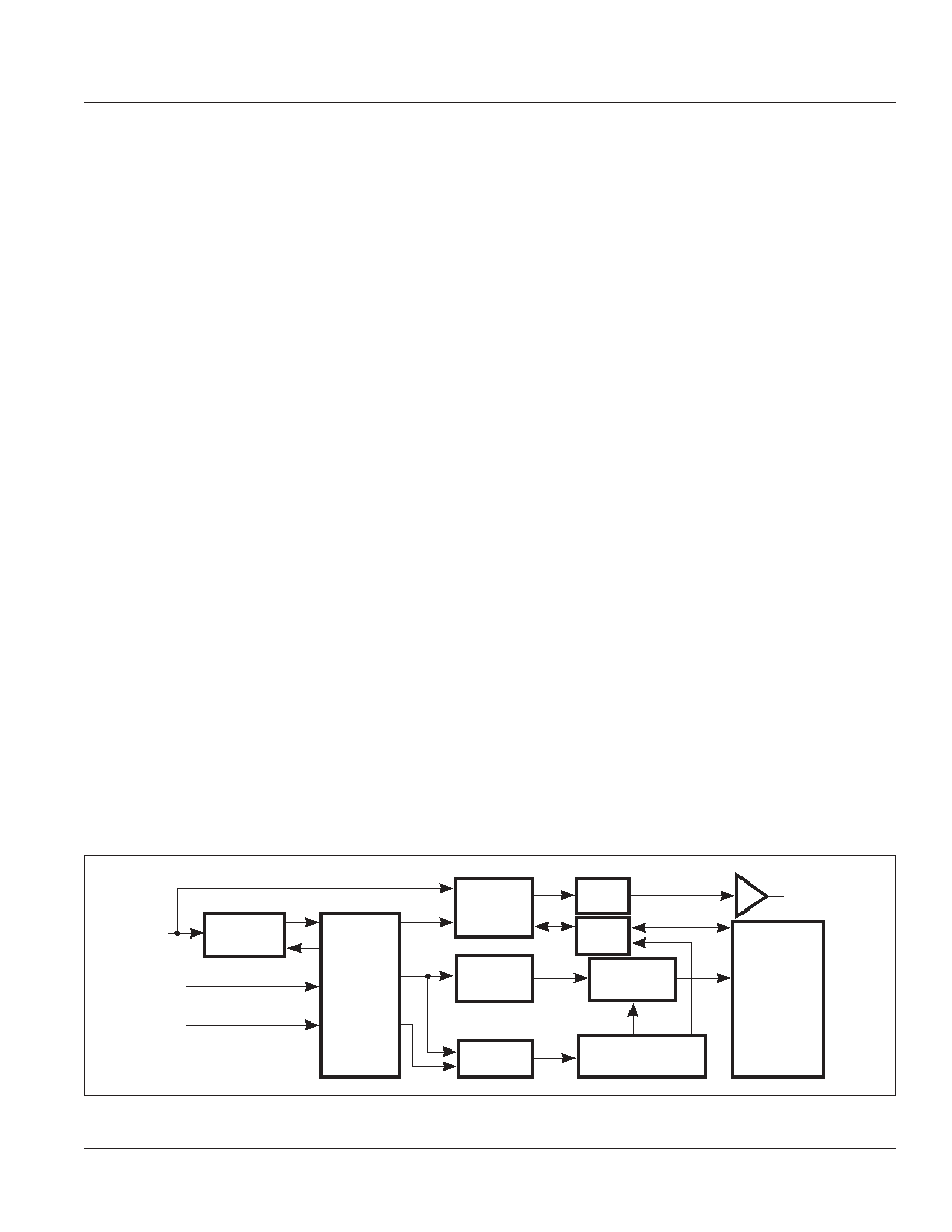
FUNCTIONAL BLOCK DIAGRAM
CS
SK
D
IN
D
OUT
DUMMY
BIT
R/W
AMPS
DATA
REGISTER
ADDRESS
REGISTER
ADDRESS
DECODER
WRITE
ENABLE
HIGH VOLTAGE
GENERATOR
INSTRUCTION
DECODE,
CONTROL,
AND
CLOCK
GENERATION
EEPROM
ARRAY
1024/2048x8
512/1024x16
INSTRUCTION
REGISTER
FEATURES
∑ Industry-standard Microwire Interface
-- Non-volatile data storage
-- Low voltage operation:
Vcc = 1.8V to 5.5V -2
Vcc = 2.5V to 5.5V -3
-- Full TTL compatible inputs and outputs
-- Auto increment for efficient data dump
∑ User Configured Memory Organization
-- By 16-bit or by 8-bit
∑ Hardware and software write protection
-- Defaults to write-disabled state at power-up
-- Software instructions for write-enable/disable
∑ Enhanced low voltage CMOS E
2
PROM
technology
∑ Versatile, easy-to-use Interface
-- Self-timed programming cycle
-- Automatic erase-before-write
-- Programming status indicator
-- Word and chip erasable
-- Chip select enables power savings
∑ Durable and reliable
-- 40-year data retention after 1M write cycles
-- 1 million write cycles
-- Unlimited read cycles
-- Schmitt-trigger Inputs
∑ Industrial and Automotive Temperature Grade
∑ Lead-free available
DESCRIPTION
IS93C76A/86A are 8kb/16kb non-volatile, ISSI
Æ
serial EEPROMs. They are fabricated using an
enhanced CMOS design and process. IS93C76A/
86A contains power-efficient read/write memory,
and organization of either 1,024/2,048 bytes of 8
bits or 512/1,024 words of 16 bits. When the
ORG pin is connected to Vcc or left unconnected,
x16 is selected; when it is connected to ground,
x8 is selected.
An instruction set defines the operation of the
devices, including read, write, and mode-enable
functions. To protect against inadvertent data
modification, all erase and write instructions are
accepted only while the device are write-enabled.
A selected x8 byte or x16 word can be modified
with a single WRITE or ERASE instruction.
Additionally, the two instructions WRITE ALL or
ERASE ALL can program an entire array. Once a
device begins its self-timed program procedure,
the data out pin (Dout) can indicate the READY/
BUSY
status by raising chip select (CS). The self-
timed write cycle includes an automatic erase-
before-write capability. The devices can output
any number of consecutive bytes/words using a
single READ instruction.
2
Integrated Silicon Solution, Inc. -- www.issi.com --
1-800-379-4774
Rev. 00F
05/26/05
IS93C76A IS93C86A
ISSI
Æ
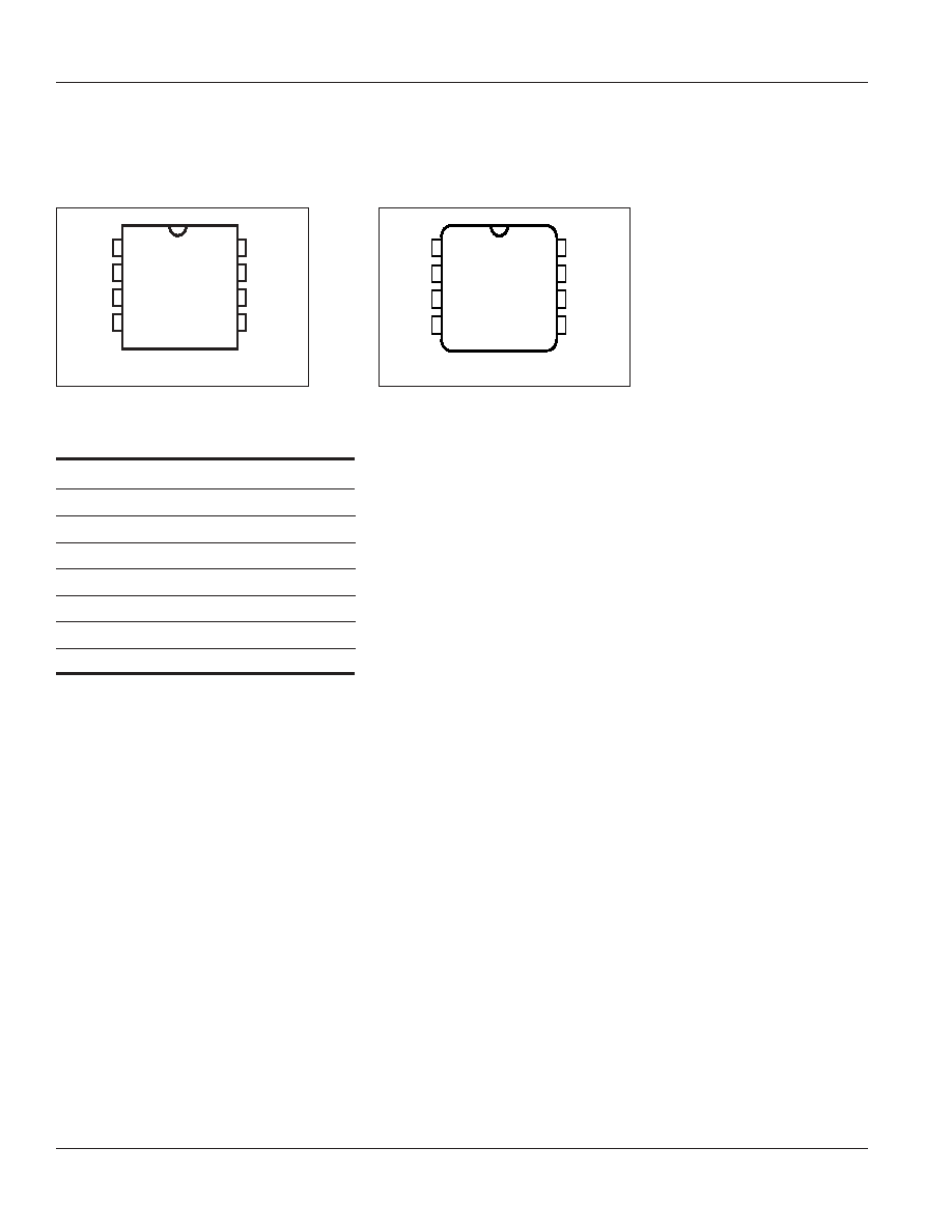
PIN CONFIGURATIONS
8-Pin JEDEC SOIC "GR"
PIN DESCRIPTIONS
CS
Chip Select
SK
Serial Data Clock
D
IN
Serial Data Input
D
OUT
Serial Data Output
ORG
Organization Select
NC
Not Connected
Vcc
Power
GND
Ground
instruction begins with a start bit of the logical "1" or
HIGH. Following this are the opcode (2 bits),
address field (10 or 11 bits), and data, if appropriate.
The clock signal may be held stable at any moment to
suspend the device at its last state, allowing clock-
speed flexibility. Upon completion of bus
communication, CS would be pulled LOW. The device
then would enter Standby mode if no internal
programming is underway.
Read (READ)
The READ instruction is the only instruction that outputs
serial data on the D
OUT
pin. After the read instruction and
address have been decoded, data is transferred from the
selected memory register into a serial shift register. (Please
note that one logical "0" bit precedes the actual 8 or 16-bit
output data string.) The output on D
OUT
changes during the
low-to-high transitions of SK (see Figure 3).
Low Voltage Read
The IS93C76A/86A are designed to ensure that data read
operations are reliable in low voltage environments. They
provide accurate operation with Vcc as low as 1.8V.
Auto Increment Read Operations
In the interest of memory transfer operation applications,
the IS93C76A/86A are designed to output a continuous
stream of memory content in response to a single read
operation instruction. To utilize this function, the system
asserts a read instruction specifying a start location ad-
dress. Once the 8 or 16 bits of the addressed register have
been clocked out, the data in consecutively higher address
locations is output. The address will wrap around continu-
ously with CS HIGH until the chip select (CS) control pin is
brought LOW. This allows for single instruction data dumps
to be executed with a minimum of firmware overhead.
Applications
The IS93C76A/86A are very popular in many
applications which require low-power, low-density
storage. Applications using these devices include
industrial controls, networking, and numerous other
consumer electronics.
Endurance and Data Retention
The IS93C76A/86A are designed for applications requiring
up to 1M programming cycles (WRITE, WRALL, ERASE
and ERAL). They provide 40 years of secure data retention
without power after the execution of 1M programming cycles.
Device Operations
The IS93C76A/86A are controlled by a set of
instructions which are clocked-in serially on the Din pin.
Before each low-to-high transition of the clock (SK), the
CS pin must have already been raised to HIGH, and the
Din value must be stable at either LOW or HIGH. Each
1
2
3
4
8
7
6
5
CS
SK
D
IN
D
OUT
VCC
NC
ORG
GND
1
2
3
4
8
7
6
5
CS
SK
D
IN
D
OUT
VCC
NC
ORG
GND
8-Pin DIP, 8-Pin TSSOP

Integrated Silicon Solution, Inc. -- www.issi.com --
1-800-379-4774
3
Rev. 00F
05/26/05
IS93C76A IS93C86A
ISSI
Æ
Write All (WRALL)
The write all (WRALL) instruction programs all registers with
the data pattern specified in the instruction. As with the
WRITE instruction, the falling edge of CS must occur to
initiate the self-timed programming cycle. If CS is then
brought HIGH after a minimum wait of 200 ns (t
CS
), the D
OUT
pin indicates the READY/
BUSY
status of the chip (see
Figure 6). Vcc is required to be above 4.5V for WRALL to
function properly.
Write Disable (WDS)
The write disable (WDS) instruction disables all programming
capabilities. This protects the entire device against acci-
dental modification of data until a WEN instruction is
executed. (When Vcc is applied, this part powers up in the
write disabled state.) To protect data, a WDS instruction
should be executed upon completion of each programming
operation.
Erase Register (ERASE)
After the erase instruction is entered, CS must be brought
LOW. The falling edge of CS initiates the self-timed internal
programming cycle. Bringing CS HIGH after a minimum of
t
CS
, will cause D
OUT
to indicate the READ/
BUSY
status of the
chip: a logical "0" indicates programming is still in progress;
a logical "1" indicates the erase cycle is complete and the
part is ready for another instruction (see Figure 8).
Erase All (ERAL)
Full chip erase is provided for ease of programming. Erasing
the entire chip involves setting all bits in the entire memory
array to a logical "1" (see Figure 9). Vcc is required to be
above 4.5V for ERALL to function properly.
Write Enable (WEN)
The write enable (WEN) instruction must be executed
before any device programming (WRITE, WRALL,
ERASE, and ERAL) can be done. When Vcc is applied,
this device powers up in the write disabled state. The
device then remains in a write disabled state until a WEN
instruction is executed. Thereafter, the device remains
enabled until a WDS instruction is executed or until Vcc
is removed. (See Figure 4.) (Note: Chip select must
remain LOW until Vcc reaches its operational value.)
Write (WRITE)
The WRITE instruction includes 8 or 16 bits of data to be
written into the specified register. After the last data bit
has been applied to D
IN
, and before the next rising edge
of SK, CS must be brought LOW. If the device is write-
enabled, then the falling edge of CS initiates the self-
timed programming cycle (see WEN).
If CS is brought HIGH, after a minimum wait of 200 ns (5V
operation) after the falling edge of CS (t
CS
) D
OUT
will
indicate the READY/
BUSY
status of the chip. Logical "0"
means programming is still in progress; logical "1" means
the selected register has been written, and the part is
ready for another instruction (see Figure 5). The READY/
BUSY
status will not be available if: a) The CS input goes
HIGH after the end of the self-timed programming cycle,
t
WP
; or b) Simultaneously CS is HIGH, Din is HIGH, and
SK goes HIGH, which clears the status flag.

4
Integrated Silicon Solution, Inc. -- www.issi.com --
1-800-379-4774
Rev. 00F
05/26/05
IS93C76A IS93C86A
ISSI
Æ
INSTRUCTION SET - IS93C76A (8kb)
8-bit Organization
16-bit Organization
(ORG = GND)
(ORG = Vcc)
Instruction
(2)
Start Bit
OP Code
Address
(1)
Input Data
Address
(1)
Input Data
READ
1
10
x(A
9
-A
0
)
--
x(A
8
-A
0
)
--
WEN
(Write Enable)
1
00
11x xxxx xxxx
--
11 xxxx xxxx
--
WRITE
1
01
x(A
9
-A
0
)
(D
7
-D
0
)
x(A
8
-A
0
)
(D
15
-D
0
)
WRALL
(Write All Registers)
1
00
01x xxxx xxxx
(D
7
-D
0
)
01 xxxx xxxx
(D
15
-D
0
)
WDS
(Write Disable)
1
00
00x xxxx xxxx
--
00 xxxx xxxx
--
ERASE
1
11
x(A
9
-A
0
)
--
x(A
8
-A
0
)
--
ERAL (
Erase All Registers)
1
00
10x xxxx xxxx
--
10 xxxx xxxx
--
Notes:
1. x = Don't care bit.
2. If the number of bits clocked-in does not match the number corresponding to a selected command, all extra trailing bits are ignored,
and WRITE, WRALL, ERASE, ERAL, WEN, and WDS instructions are rejected, but READ is accepted.
Notes:
1. x = Don't care bit.
2. If the number of bits clocked-in does not match the number corresponding to a selected command, all extra trailing bits are ignored,
and WRITE, WRALL, ERASE, ERAL, WEN, and WDS instructions are rejected, but READ is accepted.
INSTRUCTION SET - IS93C86A (16kb)
8-bit Organization
16-bit Organization
(ORG = GND)
(ORG = Vcc)
Instruction
(2)
Start Bit
OP Code
Address
(1)
Input Data
Address
(1)
Input Data
READ
1
10
(A
10
-A
0
)
--
(A
9
-A
0
)
--
WEN
(Write Enable)
1
00
11x xxxx xxxx
--
11 xxxx xxxx
--
WRITE
1
01
(A
10
-A
0
)
(D
7
-D
0
)
(A
9
-A
0
)
(D
15
-D
0
)
WRALL
(Write All Registers)
1
00
01x xxxx xxxx
(D
7
-D
0
)
01 xxxx xxxx
(D
15
-D
0
)
WDS
(Write Disable)
1
00
00x xxxx xxxx
--
00 xxxx xxxx
--
ERASE
1
11
(A
10
-A
0
)
--
(A
9
-A
0
)
--
ERAL (
Erase All Registers)
1
00
10x xxxx xxxx
--
10 xxxx xxxx
--

Integrated Silicon Solution, Inc. -- www.issi.com --
1-800-379-4774
5
Rev. 00F
05/26/05
IS93C76A IS93C86A
ISSI
Æ
CAPACITANCE
Symbol
Parameter
Conditions
Max.
Unit
C
IN
Input Capacitance
V
IN
= 0V
5
pF
C
OUT
Output Capacitance
V
OUT
= 0V
5
pF
OPERATING RANGE
R a n g e
Ambient Temperature
V
C C
Industrial
≠40∞C to +85∞C
1.8V to 5.5V or 2.5V to 5.5V
Automotive
≠40∞C to +125∞C
2.5V to 5.5V
ABSOLUTE MAXIMUM RATINGS
(1)
Symbol
Parameter
Value
Unit
V
S
Supply Voltage
≠0.5 to +6.5
V
V
P
Voltage on Any Pin
≠0.5 to Vcc + 0.5
V
T
BIAS
Temperature Under Bias
≠55 to +125
∞C
T
STG
Storage Temperature
≠65 to +150
∞C
I
OUT
Output Current
5
mA
Notes:
1. Stress greater than those listed under ABSOLUTE MAXIMUM RATINGS may cause
permanent damage to the device. This is a stress rating only and functional operation of
the device at these or any other conditions above those indicated in the operational
sections of this specification is not implied. Exposure to absolute maximum rating
conditions for extended periods may affect reliability.