
IS42S81600B
IS42S16800B
Integrated Silicon Solution, Inc. -- www.issi.com --
1-800-379-4774
1
Rev. E
05/01/06
Copyright © 2006 Integrated Silicon Solution, Inc. All rights reserved. ISSI reserves the right to make changes to this specification and its products at any
time without notice. ISSI assumes no liability arising out of the application or use of any information, products or services described herein. Customers are
advised to obtain the latest version of this device specification before relying on any published information and before placing orders for products.
ISSI
Æ
FEATURES
∑ Clock frequency: 167, 143, 133 MHz
∑ Fully synchronous; all signals referenced to a
positive clock edge
∑ Internal bank for hiding row access/precharge
∑ Power supply
V
DD
V
DDQ
IS42S81600B
3.3V
3.3V
IS42S16800B
3.3V
3.3V
∑ LVTTL interface
∑ Programmable burst length
≠ (1, 2, 4, 8, full page)
∑ Programmable burst sequence:
Sequential/Interleave
∑ Auto Refresh (CBR)
∑ Self Refresh with programmable refresh periods
∑ 4096 refresh cycles every 64 ms
∑ Random column address every clock cycle
∑ Programmable
CAS latency (2, 3 clocks)
∑ Burst read/write and burst read/single write
operations capability
∑ Burst termination by burst stop and precharge
command
∑ Industrial Temperature Availability
∑ Lead-free Availability
OVERVIEW
ISSI
's 128Mb Synchronous DRAM achieves high-speed
data transfer using pipeline architecture. All inputs and
outputs signals refer to the rising edge of the clock
input.The 128Mb SDRAM is organized as follows.
16Meg x 8, 8Meg x16
128-MBIT SYNCHRONOUS DRAM
MAY 2006
KEY TIMING PARAMETERS
Parameter
-6
-7
-75E
Unit
Clk Cycle Time
CAS Latency = 3
6
7
≠
ns
CAS Latency = 2
≠
10
7.5
ns
Clk Frequency
CAS Latency = 3
167
143
≠
Mhz
CAS Latency = 2
≠
100
133
Mhz
Access Time from Clock
CAS Latency = 3
5.4
5.4
≠
ns
CAS Latency = 2
≠
6
6
ns
IS42S81600B
IS42S16800B
4M x8x4 Banks
2M x16x4 Banks
54-pin TSOPII
54-pin TSOPII
ISSI
Æ
2
Integrated Silicon Solution, Inc. -- www.issi.com --
1-800-379-4774
Rev. E
05/01/06
IS42S81600B, IS42S16800B
DEVICE OVERVIEW
The 128Mb SDRAM is a high speed CMOS, dynamic
random-access memory designed to operate in 3.3V V
DD
and 3.3V V
DDQ
memory systems containing 134,217,728
bits. Internally configured as a quad-bank DRAM with a
synchronous interface. Each 33,554,432-bit bank is orga-
nized as 4,096 rows by 512 columns by 16 bits or 4,096 rows
by 1,024 columns by 8 bits.
The 128Mb SDRAM includes an AUTO REFRESH MODE,
and a power-saving, power-down mode. All signals are
registered on the positive edge of the clock signal, CLK. All
inputs and outputs are LVTTL compatible.
The 128Mb SDRAM has the ability to synchronously burst
data at a high data rate with automatic column-address
generation, the ability to interleave between internal banks
to hide precharge time and the capability to randomly
change column addresses on each clock cycle during
burst access.
A self-timed row precharge initiated at the end of the burst
sequence is available with the AUTO PRECHARGE func-
tion enabled. Precharge one bank while accessing one of the
other three banks will hide the precharge cycles and provide
seamless, high-speed, random-access operation.
SDRAM read and write accesses are burst oriented starting at
a selected location and continuing for a programmed num-
ber of locations in a programmed sequence. The registra-
tion of an ACTIVE command begins accesses, followed by
a READ or WRITE command. The ACTIVE command in
conjunction with address bits registered are used to select
the bank and row to be accessed (BA0, BA1 select the
bank; A0-A11 select the row). The READ or WRITE
commands in conjunction with address bits registered are
used to select the starting column location for the burst
access.
Programmable READ or WRITE burst lengths consist of 1,
2, 4 and 8 locations or full page, with a burst terminate
option.
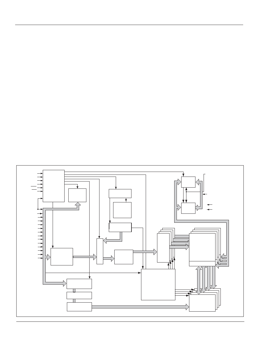
CLK
CKE
CS
RAS
CAS
WE
A9
A8
A7
A6
A5
A4
A3
A2
A1
A0
BA0
BA1
A10
COMMAND
DECODER
&
CLOCK
GENERATOR
MODE
REGISTER
REFRESH
CONTROLLER
REFRESH
COUNTER
SELF
REFRESH
CONTROLLER
ROW
ADDRESS
LATCH
MUL
TIPLEXER
COLUMN
ADDRESS LATCH
BURST COUNTER
COLUMN
ADDRESS BUFFER
COLUMN DECODER
DATA IN
BUFFER
DATA OUT
BUFFER
DQML
DQMH
DQ 0-15
V
DD
/V
DDQ
Vss/Vss
Q
12
12
9
12
12
9
16
16
16
16
512
(x 16)
4096
4096
4096
R
O
W DECODER
4096
MEMORY CELL
ARRAY
BANK 0
SENSE AMP I/O GATE
BANK CONTROL LOGIC
ROW
ADDRESS
BUFFER
A11
2
FUNCTIONAL BLOCK DIAGRAM (FOR 2MX16X4 BANKS ONLY)
Integrated Silicon Solution, Inc. -- www.issi.com --
1-800-379-4774
3
Rev. E
05/01/06
ISSI
Æ
IS42S81600B, IS42S16800B
V
DD
DQ0
V
DD
Q
NC
DQ1
V
SS
Q
NC
DQ2
V
DD
Q
NC
DQ3
V
SS
Q
NC
V
DD
NC
WE
CAS
RAS
CS
BA0
BA1
A10
A0
A1
A2
A3
V
DD
1
2
3
4
5
6
7
8
9
10
11
12
13
14
15
16
17
18
19
20
21
22
23
24
25
26
27
54
53
52
51
50
49
48
47
46
45
44
43
42
41
40
39
38
37
36
35
34
33
32
31
30
29
28
V
SS
DQ7
V
SS
Q
NC
DQ6
V
DD
Q
NC
DQ5
V
SS
Q
NC
DQ4
V
DD
Q
NC
V
SS
NC
DQM
CLK
CKE
NC
A11
A9
A8
A7
A6
A5
A4
V
SS
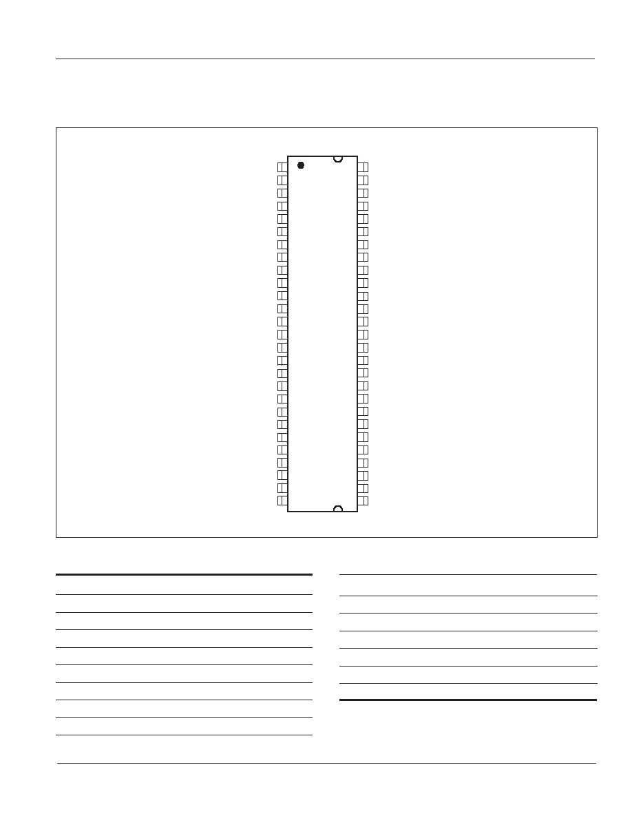
PIN CONFIGURATIONS
54 pin TSOP - Type II for x8
PIN DESCRIPTIONS
A0-A11
Row Address Input
A0-A9
Column Address Input
BA0, BA1
Bank Select Address
DQ0 to DQ7
Data I/O
CLK
System Clock Input
CKE
Clock Enable
CS
Chip Select
RAS
Row Address Strobe Command
CAS
Column Address Strobe Command
WE
Write Enable
DQM
Data Input/Output Mask
V
DD
Power
Vss
Ground
V
DDQ
Power Supply for I/O Pin
Vss
Q
Ground for I/O Pin
NC
No Connection
ISSI
Æ
4
Integrated Silicon Solution, Inc. -- www.issi.com --
1-800-379-4774
Rev. E
05/01/06
IS42S81600B, IS42S16800B
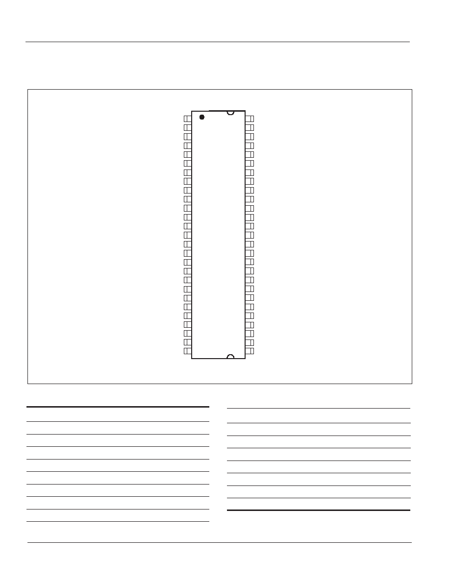
PIN CONFIGURATIONS
54 pin TSOP - Type II for x16
PIN DESCRIPTIONS
A0-A11
Row Address Input
A0-A8
Column Address Input
BA0, BA1
Bank Select Address
DQ0 to DQ15
Data I/O
CLK
System Clock Input
CKE
Clock Enable
CS
Chip Select
RAS
Row Address Strobe Command
CAS
Column Address Strobe Command
V
DD
DQ0
V
DD
Q
DQ1
DQ2
V
SS
Q
DQ3
DQ4
V
DD
Q
DQ5
DQ6
V
SS
Q
DQ7
V
DD
LDQM
WE
CAS
RAS
CS
BA0
BA1
A10
A0
A1
A2
A3
V
DD
1
2
3
4
5
6
7
8
9
10
11
12
13
14
15
16
17
18
19
20
21
22
23
24
25
26
27
54
53
52
51
50
49
48
47
46
45
44
43
42
41
40
39
38
37
36
35
34
33
32
31
30
29
28
V
SS
DQ15
V
SS
Q
DQ14
DQ13
V
DD
Q
DQ12
DQ11
V
SS
Q
DQ10
DQ9
V
DD
Q
DQ8
V
SS
NC
UDQM
CLK
CKE
NC
A11
A9
A8
A7
A6
A5
A4
V
SS
WE
Write Enable
DQML
x16 Lower Byte, Input/Output Mask
DQMH
x16 Upper Byte, Input/Output Mask
V
DD
Power
Vss
Ground
V
DDQ
Power Supply for I/O Pin
Vss
Q
Ground for I/O Pin
NC
No Connection

Integrated Silicon Solution, Inc. -- www.issi.com --
1-800-379-4774
5
Rev. E
05/01/06
ISSI
Æ
IS42S81600B, IS42S16800B
PIN FUNCTIONS
Symbol
Type
Function (In Detail)
A0-A11
Input Pin
Address Inputs: A0-A11 are sampled during the ACTIVE
command (row-address A0-A11) and READ/WRITE command (column address A0-A9
(x8), or A0-A8 (x16); with A10 defining auto precharge) to select one location out of the
memory array in the respective bank. A10 is sampled during a PRECHARGE command
to determine if all banks are to be precharged (A10 HIGH) or bank selected by
BA0, BA1 (LOW). The address inputs also provide the op-code during a LOAD MODE
REGISTER command.
BA0, BA1
Input Pin
Bank Select Address: BA0 and BA1 defines which bank the ACTIVE, READ, WRITE or
PRECHARGE command is being applied.
CAS
Input Pin
CAS, in conjunction with the RAS and WE, forms the device command. See the
"Command Truth Table" for details on device commands.
CKE
Input Pin
The CKE input determines whether the CLK input is enabled. The next rising edge of the
CLK signal will be valid when is CKE HIGH and invalid when LOW. When CKE is LOW,
the device will be in either power-down mode, clock suspend mode, or self refresh
mode. CKE is an asynchronous input.
CLK
Input Pin
CLK is the master clock input for this device. Except for CKE, all inputs to this device
are acquired in synchronization with the rising edge of this pin.
CS
Input Pin
The
CS input determines whether command input is enabled within the device.
Command input is enabled when
CS is LOW, and disabled with CS is HIGH. The device
remains in the previous state when
CS is HIGH.
DQML,
Input Pin
DQML and DQMH control the lower and upper bytes of the I/O buffers. In read
DQMH
mode,DQML and DQMH control the output buffer. WhenDQML orDQMH is LOW, the
corresponding buffer byte is enabled, and when HIGH, disabled. The outputs go to the
HIGH impedance state whenDQML/DQMH is HIGH. This function corresponds to
OE
in conventional DRAMs. In write mode,DQML and DQMH control the input buffer. When
DQML or DQMH is LOW, the corresponding buffer byte is enabled, and data can be
written to the device. WhenDQML or DQMH is HIGH, input data is masked and cannot
be written to the device. For IS42S16800B only.
DQM
Input Pin
For IS42S81600B only.
DQ
0
-DQ
7
or
Input/Output
Data on the Data Bus is latched on DQ pins during Write commands, and buffered for
DQ
0
-DQ
15
output after Read commands.
RAS
Input Pin
RAS, in conjunction with CAS and WE, forms the device command. See the "Command
Truth Table" item for details on device commands.
WE
Input Pin
WE, in conjunction with RAS and CAS, forms the device command. See the "Command
Truth Table" item for details on device commands.
V
DDQ
Power Supply Pin
V
DDQ
is the output buffer power supply.
V
DD
Power Supply Pin
V
DD
is the device internal power supply.
V
SSQ
Power Supply Pin
V
SSQ
is the output buffer ground.
V
SS
Power Supply Pin
V
SS
is the device internal ground.

ISSI
Æ
6
Integrated Silicon Solution, Inc. -- www.issi.com --
1-800-379-4774
Rev. E
05/01/06
IS42S81600B, IS42S16800B
GENERAL DESCRIPTION
READ
The READ command selects the bank from BA0, BA1
inputs and starts a burst read access to an active row.
Inputs A0-A9 (x8); A0-A8 (x16) provides the starting column
location. When A10 is HIGH, this command functions as an
AUTO PRECHARGE command. When the auto precharge
is selected, the row being accessed will be precharged at
the end of the READ burst. The row will remain open for
subsequent accesses when AUTO PRECHARGE is not
selected. DQ's read data is subject to the logic level on the
DQM inputs two clocks earlier. When a given DQM signal
was registered HIGH, the corresponding DQ's will be High-
Z two clocks later. DQ's will provide valid data when the
DQM signal was registered LOW.
WRITE
A burst write access to an active row is initiated with the
WRITE command. BA0, BA1 inputs selects the bank, and
the starting column location is provided by inputs A0-A9
(x8); A0-A8 (x16). Whether or not AUTO-PRECHARGE is
used is determined by A10.
The row being accessed will be precharged at the end of the
WRITE burst, if AUTO PRECHARGE is selected. If AUTO
PRECHARGE is not selected, the row will remain open for
subsequent accesses.
A memory array is written with corresponding input data on
DQ's and DQM input logic level appearing at the same time.
Data will be written to memory when DQM signal is LOW.
When DQM is HIGH, the corresponding data inputs will be
ignored, and a WRITE will not be executed to that byte/
column location.
PRECHARGE
The PRECHARGE command is used to deactivate the open
row in a particular bank or the open row in all banks. BA0,
BA1 can be used to select which bank is precharged or they
are treated as "Don't Care". A10 determined whether one or
all banks are precharged. After executing this command,
the next command for the selected bank(s) is executed after
passage of the period t
RP
, which is the period required for
bank precharging. Once a bank has been precharged, it is
in the idle state and must be activated prior to any READ or
WRITE commands being issued to that bank.
AUTO PRECHARGE
The AUTO PRECHARGE function ensures that the precharge
is initiated at the earliest valid stage within a burst. This
function allows for individual-bank precharge without requir-
ing an explicit command. A10 to enable the AUTO
PRECHARGE function in conjunction with a specific READ
or WRITE command. For each individual READ or WRITE
command, auto precharge is either enabled or disabled.
AUTO PRECHARGE does not apply except in full-page
burst mode. Upon completion of the READ or WRITE burst,
a precharge of the bank/row that is addressed is automati-
cally performed.
AUTO REFRESH COMMAND
This command executes the AUTO REFRESH operation.
The row address and bank to be refreshed are automatically
generated during this operation. The stipulated period (t
RC
) is
required for a single refresh operation, and no other com-
mands can be executed during this period. This command is
executed at least 4096 times for every 64ms. During an
AUTO REFRESH command, address bits are "Don't Care".
This command corresponds to CBR Auto-refresh.
BURST TERMINATE
The BURST TERMINATE command forcibly terminates the
burst read and write operations by truncating either fixed-
length or full-page bursts and the most recently registered
READ or WRITE command prior to the BURST TERMI-
NATE.
COMMAND INHIBIT
COMMAND INHIBIT prevents new commands from being
executed. Operations in progress are not affected, apart
from whether the CLK signal is enabled
NO OPERATION
When
CS is low, the NOP command prevents unwanted
commands from being registered during idle or wait states.
LOAD MODE REGISTER
During the LOAD MODE REGISTER command the mode
register is loaded from A0-A11. This command can only be
issued when all banks are idle.
ACTIVE COMMAND
When the ACTIVE COMMAND is activated, BA0, BA1
inputs selects a bank to be accessed, and the address
inputs on A0-A11 selects the row. Until a PRECHARGE
command is issued to the bank, the row remains open for
accesses.

Integrated Silicon Solution, Inc. -- www.issi.com --
1-800-379-4774
7
Rev. E
05/01/06
ISSI
Æ
IS42S81600B, IS42S16800B
CKE
DQM
Function
n-1
n
U
L
Data write / output enable
H
◊
L
L
Data mask / output disable
H
◊
H
H
Upper byte write enable / output enable
H
◊
L
◊
Lower byte write enable / output enable
H
◊
◊
L
Upper byte write inhibit / output disable
H
◊
H
◊
Lower byte write inhibit / output disable
H
◊
◊
H
CKE
A11
Function
n ≠ 1
n
CS
CS
CS
CS
CS
RAS
RAS
RAS
RAS
RAS
CAS
CAS
CAS
CAS
CAS
WE
WE
WE
WE
WE
BA1
BA0
A10
A9 - A0
Device deselect (DESL)
H
◊
H
◊
◊
◊
◊
◊
◊
◊
No operation (NOP)
H
◊
L
H
H
H
◊
◊
◊
◊
Burst stop (BST)
H
◊
L
H
H
L
◊
◊
◊
◊
Read
H
◊
L
H
L
H
V
V
L
V
Read with auto precharge
H
◊
L
H
L
H
V
V
H
V
Write
H
◊
L
H
L
L
V
V
L
V
Write with auto precharge
H
◊
L
H
L
L
V
V
H
V
Bank activate (ACT)
H
◊
L
L
H
H
V
V
V
V
Precharge select bank (PRE) H
◊
L
L
H
L
V
V
L
◊
Precharge all banks (PALL)
H
◊
L
L
H
L
◊
◊
H
◊
CBR Auto-Refresh (REF)
H
H
L
L
L
H
◊
◊
◊
◊
Self-Refresh (SELF)
H
L
L
L
L
H
◊
◊
◊
◊
Mode register set (MRS)
H
◊
L
L
L
L
L
L
L
V
COMMAND TRUTH TABLE
DQM TRUTH TABLE
Note: H=V
IH
, L=V
IL
x= V
IH
or V
IL
, V = Valid Data.
Note: H=V
IH
, L=V
IL
x= V
IH
or V
IL
, V = Valid Data.

ISSI
Æ
8
Integrated Silicon Solution, Inc. -- www.issi.com --
1-800-379-4774
Rev. E
05/01/06
IS42S81600B, IS42S16800B
CKE
Current State /Function
n ≠ 1 n
CS
RAS
CAS WE
Address
Activating Clock suspend mode entry
H
L
◊
◊
◊
◊
◊
Any Clock suspend mode
L
L
◊
◊
◊
◊
◊
Clock suspend mode exit
L
H
◊
◊
◊
◊
◊
Auto refresh command Idle (REF)
H
H
L
L
L
H
◊
Self refresh entry Idle (SELF)
H
L
L
L
L
H
◊
Power down entry Idle
H
L
◊
◊
◊
◊
◊
Self refresh exit
L
H
L
H
H
H
◊
L
H
H
◊
◊
◊
◊
Power down exit
L
H
◊
◊
◊
◊
◊
Note: H=V
IH
, L=V
IL
x= V
IH
or V
IL
, V = Valid Data.
CKE TRUTH TABLE

Integrated Silicon Solution, Inc. -- www.issi.com --
1-800-379-4774
9
Rev. E
05/01/06
ISSI
Æ
IS42S81600B, IS42S16800B
Current State
CS
CS
CS
CS
CS
RAS
RAS
RAS
RAS
RAS CAS
CAS
CAS
CAS
CAS
WE
WE
WE
WE
WE
Address
Command
Action
Idle
H
X
X
X
X
DESL
Nop or Power Down
(2)
L
H
H
H
X
NOP
Nop or Power Down
(2)
L
H
H
L
X
BST
Nop or Power Down
L
H
L
H
BA, CA, A10
READ/READA
ILLEGAL
(3)
L
H
L
L
A, CA, A10
WRIT/ WRITA
ILLEGAL
(3)
L
L
H
H
BA, RA
ACT
Row activating
L
L
H
L
BA, A10
PRE/PALL
Nop
L
L
L
H
X
REF/SELF
Auto refresh or Self-refresh
(4)
L
L
L
L
OC, BA1=L
MRS
Mode register set
Row Active
H
X
X
X
X
DESL
Nop
L
H
H
H
X
NOP
Nop
L
H
H
L
X
BST
Nop
L
H
L
H
BA, CA, A10
READ/READA
Begin read
(5)
L
H
L
L
BA, CA, A10
WRIT/ WRITA
Begin write
(5)
L
L
H
H
BA, RA
ACT
ILLEGAL
(3)
L
L
H
L
BA, A10
PRE/PALL
Precharge
Precharge all banks
(6)
L
L
L
H
X
REF/SELF
ILLEGAL
L
L
L
L
OC, BA
MRS
ILLEGAL
Read
H
X
X
X
X
DESL
Continue burst to end to
Row active
L
H
H
H
X
NOP
Continue burst to end Row
Row active
L
H
H
L
X
BST
Burst stop, Row active
L
H
L
H
BA, CA, A10
READ/READA
Terminate burst,
begin new read
(7)
L
H
L
L
BA, CA, A10
WRIT/WRITA
Terminate burst,
begin write
(7,8)
L
L
H
H
BA, RA
ACT
ILLEGAL
(3)
L
L
H
L
BA, A10
PRE/PALL
Terminate burst
Precharging
L
L
L
H
X
REF/SELF
ILLEGAL
L
L
L
L
OC, BA
MRS
ILLEGAL
Write
H
X
X
X
X
DESL
Continue burst to end
Write recovering
L
H
H
H
X
NOP
Continue burst to end
Write recovering
L
H
H
L
X
BST
Burst stop, Row active
L
H
L
H
BA, CA, A10
READ/READA
Terminate burst, start read :
Determine AP
(7,8)
L
H
L
L
BA, CA, A10
WRIT/WRITA
Terminate burst, new write :
Determine AP
(7)
L
L
H
H
BA, RA
RA ACT
ILLEGAL
(3)
L
L
H
L
BA, A10
PRE/PALL
Terminate burst Precharging
(9)
L
L
L
H
X
REF/SELF
ILLEGAL
L
L
L
L
OC, BA
MRS
ILLEGAL
FUNCTIONAL TRUTH TABLE
Note: H=V
IH
, L=V
IL
x= V
IH
or V
IL
, V = Valid Data, BA= Bank Address, CA+Column Address, RA=Row Address, OC= Op-Code

ISSI
Æ
10
Integrated Silicon Solution, Inc. -- www.issi.com --
1-800-379-4774
Rev. E
05/01/06
IS42S81600B, IS42S16800B
Current State
CS
CS
CS
CS
CS
RAS
RAS
RAS
RAS
RAS CAS
CAS
CAS
CAS
CAS
WE
WE
WE
WE
WE
Address
Command
Action
Read with auto
H
◊
◊
◊
◊
DESL
Continue burst to end, Precharge
Precharging
L
H
H
H
x
NOP
Continue burst to end, Precharge
L
H
H
L
◊
BST
ILLEGAL
L
H
L
H
BA, CA, A10
READ/READA
ILLEGAL
(11)
L
H
L
L
BA, CA, A10
WRIT/ WRITA
ILLEGAL
(11)
L
L
H
H
BA, RA
ACT
ILLEGAL
(3)
L
L
H
L
BA, A10
PRE/PALL
ILLEGAL
(11)
L
L
L
H
◊
REF/SELF
ILLEGAL
L
L
L
L
OC, BA
MRS
ILLEGAL
Write with Auto
H
◊
◊
◊
◊
DESL
Continue burst to end, Write
Precharge
recovering with auto precharge
L
H
H
H
◊
NOP
Continue burst to end, Write
recovering with auto precharge
L
H
H
L
◊
BST
ILLEGAL
L
H
L
H
BA, CA, A10
READ/READA
ILLEGAL
(11)
L
H
L
L
BA, CA, A10
WRIT/ WRITA
ILLEGAL
(11)
L
L
H
H
BA, RA
ACT
ILLEGAL
(3,11)
L
L
H
L
BA, A10
PRE/PALL
ILLEGAL
(3,11)
L
L
L
H
◊
REF/SELF
ILLEGAL
L
L
L
L
OC, BA
MRS
ILLEGAL
Precharging
H
◊
◊
◊
◊
DESL
Nop, Enter idle after tRP
L
H
H
H
◊
NOP
Nop, Enter idle after tRP
L
H
H
L
◊
BST
Nop, Enter idle after tRP
L
H
L
H
BA, CA, A10
READ/READA
ILLEGAL
(3)
L
H
L
L
BA, CA, A10
WRIT/WRITA
ILLEGAL
(3)
L
L
H
H
BA, RA
ACT
ILLEGAL
(3)
L
L
H
L
BA, A10
PRE/PALL
Nop Enter idle after tRP
L
L
L
H
◊
REF/SELF
ILLEGAL
L
L
L
L
OC, BA
MRS
ILLEGAL
Row Activating
H
◊
◊
◊
◊
DESL
Nop, Enter bank active after tRCD
L
H
H
H
◊
NOP
Nop, Enter bank active after tRCD
L
H
H
L
◊
BST
Nop, Enter bank active after tRCD
L
H
L
H
BA, CA, A10
READ/READA
ILLEGAL
(3)
L
H
L
L
BA, CA, A10
WRIT/WRITA
ILLEGAL
(3)
L
L
H
H
BA, RA
ACT
ILLEGAL
(3,9)
L
L
H
L
BA, A10
PRE/PALL
ILLEGAL
(3)
L
L
L
H
◊
REF/SELF
ILLEGAL
L
L
L
L
OC, BA
MRS
ILLEGAL
FUNCTIONAL TRUTH TABLE Continued:
Note: H=V
IH
, L=V
IL
x= V
IH
or V
IL
, V = Valid Data, BA= Bank Address, CA+Column Address, RA=Row Address, OC= Op-Code

Integrated Silicon Solution, Inc. -- www.issi.com --
1-800-379-4774
11
Rev. E
05/01/06
ISSI
Æ
IS42S81600B, IS42S16800B
Current State
CS
CS
CS
CS
CS
RAS
RAS
RAS
RAS
RAS CAS
CAS
CAS
CAS
CAS
WE
WE
WE
WE
WE
Address
Command
Action
Write Recovering
H
◊
◊
◊
◊
DESL
Nop, Enter row active after tDPL
L
H
H
H
◊
NOP
Nop, Enter row active after tDPL
L
H
H
L
◊
BST
Nop, Enter row active after tDPL
L
H
L
H
BA, CA, A10
READ/READA
Begin read
(8)
L
H
L
L
BA, CA, A10
WRIT/ WRITA
Begin new write
L
L
H
H
BA, RA
ACT
ILLEGAL
(3)
L
L
H
L
BA, A10
PRE/PALL
ILLEGAL
(3)
L
L
L
H
◊
REF/SELF
ILLEGAL
L
L
L
L
OC, BA
MRS
ILLEGAL
Write Recovering
H
◊
◊
◊
◊
DESL
Nop, Enter precharge after tDPL
with Auto
L
H
H
H
◊
NOP
Nop, Enter precharge after tDPL
Precharge
L
H
H
L
◊
BST
Nop, Enter row active after tDPL
L
H
L
H
BA, CA, A10
READ/READA
ILLEGAL
(3,8,11)
L
H
L
L
BA, CA, A10
WRIT/WRITA
ILLEGAL
(3,11)
L
L
H
H
BA, RA
ACT
ILLEGAL
(3,11)
L
L
H
L
BA, A10
PRE/PALL
ILLEGAL
(3,11)
L
L
L
H
◊
REF/SELF
ILLEGAL
L
L
L
L
OC, BA
MRS
ILLEGAL
Refresh
H
◊
◊
◊
◊
DESL
Nop, Enter idle after tRC
L
H
H
◊
◊
NOP/BST
Nop, Enter idle after tRC
L
H
L
H
BA, CA, A10
READ/READA
ILLEGAL
L
H
L
L
BA, CA, A10
WRIT/WRITA
ILLEGAL
L
L
H
H
BA, RA
ACT
ILLEGAL
L
L
H
L
BA, A10
PRE/PALL
ILLEGAL
L
L
L
H
◊
REF/SELF
ILLEGAL
L
L
L
L
OC, BA
MRS
ILLEGAL
Mode Register
H
◊
◊
◊
◊
DESL
Nop, Enter idle after 2 clocks
Accessing
L
H
H
H
◊
NOP
Nop, Enter idle after 2 clocks
L
H
H
L
◊
BST
ILLEGAL
L
H
L
◊
BA, CA, A10
READ/WRITE
ILLEGAL
L
L
◊
◊
BA, RA
ACT/PRE/PALL
ILLEGAL
REF/MRS
FUNCTIONAL TRUTH TABLE Continued:
Note: H=V
IH
, L=V
IL
x= V
IH
or V
IL
, V = Valid Data, BA= Bank Address, CA+Column Address, RA=Row Address, OC= Op-Code
Notes:
1. All entries assume that CKE is active (CKEn-1=CKEn=H).
2. If both banks are idle, and CKE is inactive (Low), the device will enter Power Down mode. All input buffers except CKE will
be disabled.
3. Illegal to bank in specified states; Function may be legal in the bank indicated by Bank Address (BA), depending on the
state of that bank.
4. If both banks are idle, and CKE is inactive (Low), the device will enter Self-Refresh mode. All input buffers except CKE will
be disabled.
5. Illegal if tRCD is not satisfied.
6. Illegal if tRAS is not satisfied.
7. Must satisfy burst interrupt condition.
8. Must satisfy bus contention, bus turn around, and/or write recovery requirements.
9. Must mask preceding data which don't satisfy tDPL.
10. Illegal if tRRD is not satisfied.
11. Illegal for single bank, but legal for other banks.

ISSI
Æ
12
Integrated Silicon Solution, Inc. -- www.issi.com --
1-800-379-4774
Rev. E
05/01/06
IS42S81600B, IS42S16800B
CKE RELATED COMMAND TRUTH TABLE
(1)
CKE
Current State
Operation
n-1
n
CS
RAS
CAS
WE Address
Self-Refresh (S.R.)
INVALID, CLK (n - 1) would exit S.R.
H
X
X
X
X
X
X
Self-Refresh Recovery
(2)
L
H
H
X
X
X
X
Self-Refresh Recovery
(2)
L
H
L
H
H
X
X
Illegal
L
H
L
H
L
X
X
Illegal
L
H
L
L
X
X
X
Maintain S.R.
L
L
X
X
X
X
X
Self-Refresh Recovery
Idle After t
RC
H
H
H
X
X
X
X
Idle After t
RC
H
H
L
H
H
X
X
Illegal
H
H
L
H
L
X
X
Illegal
H
H
L
L
X
X
X
Begin clock suspend next cycle
(5)
H
L
H
X
X
X
X
Begin clock suspend next cycle
(5)
H
L
L
H
H
X
X
Illegal
H
L
L
H
L
X
X
Illegal
H
L
L
L
X
X
X
Exit clock suspend next cycle
(2)
L
H
X
X
X
X
X
Maintain clock suspend
L
L
X
X
X
X
X
Power-Down (P.D.)
INVALID, CLK (n - 1) would exit P.D.
H
X
X
X
X
X
--
EXIT P.D. --> Idle
(2)
L
H
X
X
X
X
X
Maintain power down mode
L
L
X
X
X
X
X
Both Banks Idle
Refer to operations in Operative Command Table
H
H
H
X
X
X
--
Refer to operations in Operative Command Table
H
H
L
H
X
X
--
Refer to operations in Operative Command Table
H
H
L
L
H
X
--
Auto-Refresh
H
H
L
L
L
H
X
Refer to operations in Operative Command Table
H
H
L
L
L
L
Op - Code
Refer to operations in Operative Command Table
H
L
H
X
X
X
--
Refer to operations in Operative Command Table
H
L
L
H
X
X
--
Refer to operations in Operative Command Table
H
L
L
L
H
X
--
Self-Refresh
(3)
H
L
L
L
L
H
X
Refer to operations in Operative Command Table
H
L
L
L
L
L
Op - Code
Power-Down
(3)
L
X
X
X
X
X
X
Any state
Refer to operations in Operative Command Table
H
H
X
X
X
X
X
other than
Begin clock suspend next cycle
(4)
H
L
X
X
X
X
X
listed above
Exit clock suspend next cycle
L
H
X
X
X
X
X
Maintain clock suspend
L
L
X
X
X
X
X
Notes:
1. H : High level, L : low level, X : High or low level (Don't care).
2. CKE Low to High transition will re-enable CLK and other inputs asynchronously. A minimum
setup time must be satisfied
before any command other than EXIT.
3. Power down and Self refresh can be entered only from the both banks idle state.
4. Must be legal command as defined in Operative Command Table.
5. Illegal if t
SRX
is not satisfied.

Integrated Silicon Solution, Inc. -- www.issi.com --
1-800-379-4774
13
Rev. E
05/01/06
ISSI
Æ
IS42S81600B, IS42S16800B
Mode
Register
Set
IDLE
Self
Refresh
CBR (Auto)
Refresh
Row
Active
Active
Power
Down
Power
Down
WRITE
WRITE
SUSPEND
READ
READ
SUSPEND
WRITEA
SUSPEND
WRITEA
READA
READA
SUSPEND
POWER
ON
Precharge
Automatic sequence
Manual Input
SELF
SELF exit
REF
MRS
ACT
CKE
CKE
CKE
CKE
BST
Read
Write
Write
Precharge
RRE (Prec
harge term
inatio
n)
PRE (P
recharge termin
ation)
Write with
Auto Precharge
Read with
Auto Precharge
Read
Write
BST
CKE
CKE
CKE
CKE
CKE
CKE
CKE
CKE
Read
STATE DIAGRAM

ISSI
Æ
14
Integrated Silicon Solution, Inc. -- www.issi.com --
1-800-379-4774
Rev. E
05/01/06
IS42S81600B, IS42S16800B
ABSOLUTE MAXIMUM RATINGS
(1)
Symbol
Parameters
Rating
Unit
V
DD
MAX
Maximum Supply Voltage
≠0.5 to +4.6
V
V
DDQ
MAX
Maximum Supply Voltage for Output Buffer
≠0.5 to +4.6
V
V
IN
Input Voltage
≠0.5 to V
DD
+ 0.5
V
V
OUT
Output Voltage
≠1.0 to V
DDQ
+ 0.5
V
P
D
MAX
Allowable Power Dissipation
1
W
I
CS
Output Shorted Current
50
mA
T
OPR
Operating Temperature
Com.
0 to +70
∞C
Ind.
≠40 to +85
T
STG
Storage Temperature
≠65 to +150
∞C
DC RECOMMENDED OPERATING CONDITIONS
Symbol
Parameter
Min.
Typ.
Max.
Unit
V
DD
Supply Voltage
3.0
3.3
3.6
V
V
DDQ
I/O Supply Voltage
3.0
3.3
3.6
V
V
IH
(1)
Input High Voltage
2.0
--
V
DDQ
+ 1.2
V
V
IL
(2)
Input Low Voltage
-1.2
--
+0.8
V
CAPACITANCE CHARACTERISTICS
(At T
A
= 0 to +25∞C, V
DD
= V
DDQ
= 3.3 ± 0.3V)
Symbol
Parameter
Min.
Max.
Unit
-6
-7/-75E
C
IN1
Input Capacitance: CLK
2.5
3.5
4.0
pF
C
IN2
Input Capacitance:All other input pins
2.5
3.8
5.0
pF
CI/O
Data Input/Output Capacitance:I/Os
4.0
6.5
6.5
pF
Note:
1. V
IH
(max) = V
DDQ
+1.2V (
PULSE
WIDTH
< 3
NS
).
2. V
IL
(min) = -1.2V (
PULSE
WIDTH
< 3
NS
).
3. All voltages are referenced to Vss.
Notes:
1. Stress greater than those listed under ABSOLUTE MAXIMUM RATINGS may cause permanent damage to
the device. This is a stress rating only and functional operation of the device at these or any other condi-
tions above those indicated in the operational sections of this specification is not implied. Exposure to
absolute maximum rating conditions for extended periods may affect reliability.
2. All voltages are referenced to Vss.

Integrated Silicon Solution, Inc. -- www.issi.com --
1-800-379-4774
15
Rev. E
05/01/06
ISSI
Æ
IS42S81600B, IS42S16800B
DC ELECTRICAL CHARACTERISTICS 1
(Recommended Operation Conditions unless otherwise noted.)
Symbol
Parameter
Test Condition
-6
-7
-75E
Unit
I
DD1
(1)
Operating Current
One bank active, CL = 3, BL = 1,
x8
120
100
100
mA
t
CLK
= t
CLK
(min), t
RC
= t
RC
(min)
x16
140
120
120
mA
I
DD2P
Precharge Standby Current
CKE
V
IL
(
MAX
), t
CK
= 15ns
x8 / x16
2
2
2
mA
(In Power-Down Mode)
I
DD2PS
Precharge Standby Current
CKE
V
IL
(
MAX
), CLK
V
IL
(
MAX
)
x8 / x16
1
1
1
mA
(In Power-Down Mode)
I
DD2N
(2)
Precharge Standby Current
CS
Vcc - 0.2V, CKE V
IH
(
MIN
)
x8 / x16
25
25
25
mA
(In Non Power-Down Mode)
t
CK
= 15ns
I
DD2NS
Precharge Standby Current
CS
Vcc - 0.2V, CKE V
IH
(
MIN
) or
x8 / x16
15
15
15
mA
(In Non Power-Down Mode)
CKE
V
IL
(
MAX
), All inputs stable
I
DD3N
(2)
Active Standby Current
CS
Vcc - 0.2V, CKE V
IH
(
MIN
)
x8 / x16
30
30
30
mA
(In Non Power-Down Mode)
t
CK
= 15ns
I
DD3NS
Active Standby Current
CS
Vcc - 0.2V, CKE V
IH
(
MIN
) or
x8 / x16
20
20
20
mA
(In Non Power-Down Mode)
CKE
V
IL
(
MAX
), All inputs stable
I
DD4
Operating Current
All banks active, BL = 4, CL = 3,
x8
170
120
120
mA
t
CK
= t
CK
(min)
x16
180
130
130
mA
I
DD5
Auto-Refresh Current
t
RC
= t
RC
(min), t
CLK
= t
CLK
(min)
x8/ x16
180
160
160
mA
I
DD6
Self-Refresh Current
CKE
0.2V
x8 / x16
2
2
2
mA
Notes:
1. I
DD
(
MAX
) is specified at the output open condition.
2. Input signals are changed one time during 30ns.
DC ELECTRICAL CHARACTERISTICS 2
(Recommended Operation Conditions unless otherwise noted.)
Symbol
Parameter
Test Condition
Min
Max
Unit
I
IL
Input Leakage Current
0V
Vin Vcc, with pins other than
-10
10
A
the tested pin at 0V
I
OL
Output Leakage Current
Output is disabled, 0V
Vout Vcc,
-5
5
A
V
OH
Output High Voltage Level
I
OH
= -2mA
2.4
--
V
V
OL
Output Low Voltage Level
I
OL
= 2mA
--
0.4
V

ISSI
Æ
16
Integrated Silicon Solution, Inc. -- www.issi.com --
1-800-379-4774
Rev. E
05/01/06
IS42S81600B, IS42S16800B
AC ELECTRICAL CHARACTERISTICS
(1,2,3)
-6
-7
-75E
Symbol Parameter
Min.
Max.
Min.
Max.
Min.
Max.
Units
t
CK3
Clock Cycle Time
CAS Latency = 3
6
--
7
--
--
--
ns
t
CK2
CAS Latency = 2
--
--
10
--
7.5
--
ns
t
AC3
Access Time From CLK
CAS Latency = 3
--
5.4
--
5.4
--
--
ns
t
AC2
CAS Latency = 2
--
--
--
6
--
6
ns
t
CHI
CLK HIGH Level Width
2.5
--
2.5
--
2.5
--
ns
t
CL
CLK LOW Level Width
2.5
--
2.5
--
2.5
--
ns
t
OH3
Output Data Hold Time
CAS Latency = 3
2.7
--
2.7
--
--
--
ns
t
OH2
CAS Latency = 2
--
--
2.7
--
2.7
--
ns
t
LZ
Output LOW Impedance Time
0
--
0
--
0
--
ns
t
HZ
Output HIGH Impedance Time
2.7
5.4
2.7
5.4
2.7
5.4
ns
t
DS
Input Data Setup Time
(2)
1.5
--
1.5
--
1.5
--
ns
t
DH
Input Data Hold Time
(2)
0.8
--
0.8
--
0.8
--
ns
t
AS
Address Setup Time
(2)
1.5
--
1.5
--
1.5
--
ns
t
AH
Address Hold Time
(2)
0.8
--
0.8
--
0.8
--
ns
t
CKS
CKE Setup Time
(2)
1.5
--
1.5
--
1.5
--
ns
t
CKH
CKE Hold Time
(2)
0.8
--
0.8
--
0.8
--
ns
t
CS
Command Setup Time (
CS, RAS, CAS, WE, DQM)
(2)
1.5
--
1.5
--
1.5
--
ns
t
CH
Command Hold Time (
CS, RAS, CAS, WE, DQM)
(2)
0.8
--
0.8
--
0.8
--
ns
t
RC
Command Period (REF to REF / ACT to ACT)
60
--
67.5
--
67.5
--
ns
t
RAS
Command Period (ACT to PRE)
42
100K
45
100K
45
100K
ns
t
RP
Command Period (PRE to ACT)
18
--
20
--
20
--
ns
t
RCD
Active Command To Read / Write Command Delay Time 15
--
20
--
20
--
ns
t
RRD
Command Period (ACT [0] to ACT[1])
12
--
14
--
14
--
ns
t
DPL
Input Data To Precharge
12
--
14
--
14
--
ns
Command Delay time
t
DAL
Input Data To Active / Refresh
27
--
35
--
35
--
ns
Command Delay time (During Auto-Precharge)
t
MRD
Mode Register Program Time
12
--
15
--
15
--
ns
t
DDE
Power Down Exit Setup Time
6
--
7.5
--
7.5
--
ns
t
SRX
Self-Refresh Exit Time
6
--
7.5
--
7.5
--
ns
t
T
Transition Time
1
10
1
10
1
10
ns
t
REF
Refresh Cycle Time (4096)
--
64
--
64
--
64
ms
Notes:
1. The power-on sequence must be executed before starting memory operation.
2. Measured with t
T
= 1 ns. If clock rising time is longer than 1ns, (t
R
/2 - 0.5) ns should be added to the parameter.
3. The reference level is 1.4V when measuring input signal timing. Rise and fall times are measured between V
IH
(min.) and V
IL
(max).

Integrated Silicon Solution, Inc. -- www.issi.com --
1-800-379-4774
17
Rev. E
05/01/06
ISSI
Æ
IS42S81600B, IS42S16800B
OPERATING FREQUENCY / LATENCY RELATIONSHIPS
SYMBOL PARAMETER
UNITS
--
Clock Cycle Time
6
7
7.5
10
ns
--
Operating Frequency (
CAS Latency = 3)
167
143
133
100
MHz
t
CAC
CAS Latency
3
3
2
2
cycle
t
RCD
Active Command To Read/Write Command Delay Time
3
3
3
2
cycle
t
RAC
RAS Latency (t
RCD
+ t
CAC
)
CAS Latency = 3
6
6
--
--
cycle
CAS Latency = 2
--
--
5
4
t
RC
Command Period (REF to REF / ACT to ACT)
10
10
9
7
cycle
t
RAS
Command Period (ACT to PRE)
7
7
6
5
cycle
t
RP
Command Period (PRE to ACT)
3
3
3
2
cycle
t
RRD
Command Period (ACT[0] to ACT [1])
2
2
2
2
cycle
t
CCD
Column Command Delay Time
1
1
1
1
cycle
(READ, READA, WRIT, WRITA)
t
DPL
Input Data To Precharge Command Delay Time
2
2
2
2
cycle
t
DAL
Input Data To Active/Refresh Command Delay Time
5
5
5
4
cycle
(During Auto-Precharge)
t
RBD
Burst Stop Command To Output in HIGH-Z Delay Time
CAS Latency = 3
3
3
--
--
cycle
(Read)
CAS Latency = 2
--
--
2
2
t
WBD
Burst Stop Command To Input in Invalid Delay Time
0
0
0
0
cycle
(Write)
t
RQL
Precharge Command To Output in HIGH-Z Delay Time
CAS Latency = 3
3
3
--
--
cycle
(Read)
CAS Latency = 2
--
--
2
2
t
WDL
Precharge Command To Input in Invalid Delay Time
0
0
0
0
cycle
(Write)
t
PQL
Last Output To Auto-Precharge Start Time (Read)
CAS Latency = 3
-2
≠2
--
--
cycle
CAS Latency = 2
--
--
-1
-1
t
QMD
DQM To Output Delay Time (Read)
2
2
2
2
cycle
t
DMD
DQM To Input Delay Time (Write)
0
0
0
0
cycle
t
MRD
Mode Register Set To Command Delay Time
2
2
2
2
cycle
ISSI
Æ
18
Integrated Silicon Solution, Inc. -- www.issi.com --
1-800-379-4774
Rev. E
05/01/06
IS42S81600B, IS42S16800B
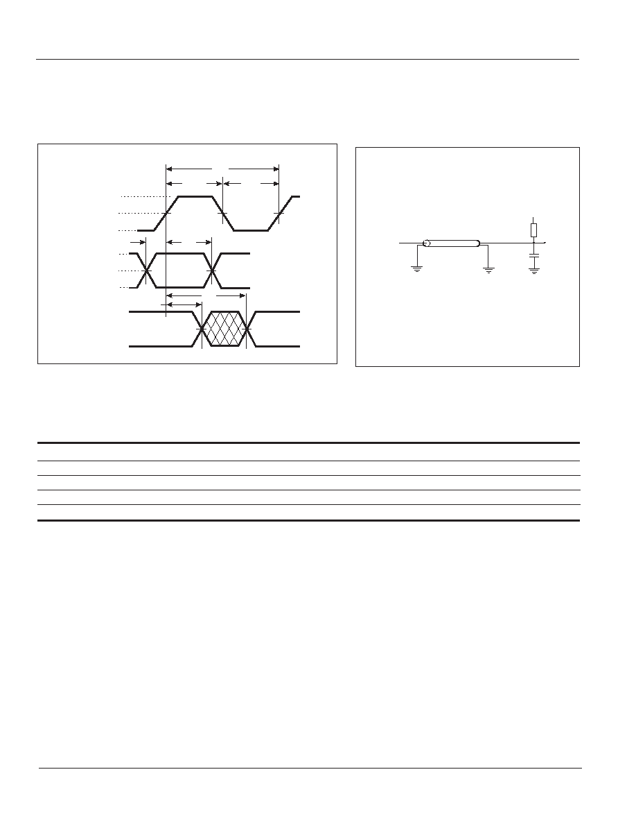
AC TEST CONDITIONS
Input Load
Output Load
Output
Z
= 50
50 pF
1.4V
50
3.0V
1.4V
0V
CLK
INPUT
OUTPUT
t
CHI
t
CH
t
AC
t
OH
t
CS
t
CK
t
CL
3.0V
1.4V
1.4V
1.4V
0V
AC TEST CONDITIONS
Parameter
Rating
AC Input Levels
0V to 3.0V
Input Rise and Fall Times
1 ns
Input Timing Reference Level
1.4V
Output Timing Measurement Reference Level
1.4V

Integrated Silicon Solution, Inc. -- www.issi.com --
1-800-379-4774
19
Rev. E
05/01/06
ISSI
Æ
IS42S81600B, IS42S16800B
FUNCTIONAL DESCRIPTION
The 128Mb SDRAMs are quad-bank DRAMs which operate
at 3.3V and include a synchronous interface (all signals are
registered on the positive edge of the clock signal, CLK).
Each of the 33,554,432-bit banks is organized as 4,096
rows by 512 columns by 16 bits or 4,096 rows by 1,024
columns by 8 bits.
Read and write accesses to the SDRAM are burst oriented;
accesses start at a selected location and continue for a
programmed number of locations in a programmed
sequence. Accesses begin with the registration of an AC-
TIVE command which is then followed by a READ or WRITE
command. The address bits registered coincident with the
ACTIVE command are used to select the bank and row to
be accessed (BA0 and BA1 select the bank, A0-A11 select the row).
The address bits A0-A9 (x8); A0-A8 (x16) registered coincident
with the READ or WRITE command are used to select the
starting column location for the burst access.
Prior to normal operation, the SDRAM must be initialized.
The following sections provide detailed information covering
device initialization, register definition, command
descriptions and device operation.
Initialization
SDRAMs must be powered up and initialized in a
predefined manner.
The 128M SDRAM is initialized after the power is applied to
V
DD
and V
DDQ
(simultaneously) and the clock is stable with
DQM High and CKE High.
A 100µs delay is required prior to issuing any command
other than a COMMAND INHIBIT or a NOP. The COMMAND
INHIBIT or NOP may be applied during the 100us period and
should continue at least through the end of the period.
With at least one COMMAND INHIBIT or NOP command
having been applied, a PRECHARGE command should be
applied once the 100µs delay has been satisfied. All banks
must be precharged. This will leave all banks in an idle state
after which at least two AUTO REFRESH cycles must be
performed. After the AUTO REFRESH cycles are complete,
the SDRAM is then ready for mode register programming.
The mode register should be loaded prior to applying any
operational command because it will power up in an un-
known state.
ISSI
Æ
20
Integrated Silicon Solution, Inc. -- www.issi.com --
1-800-379-4774
Rev. E
05/01/06
IS42S81600B, IS42S16800B
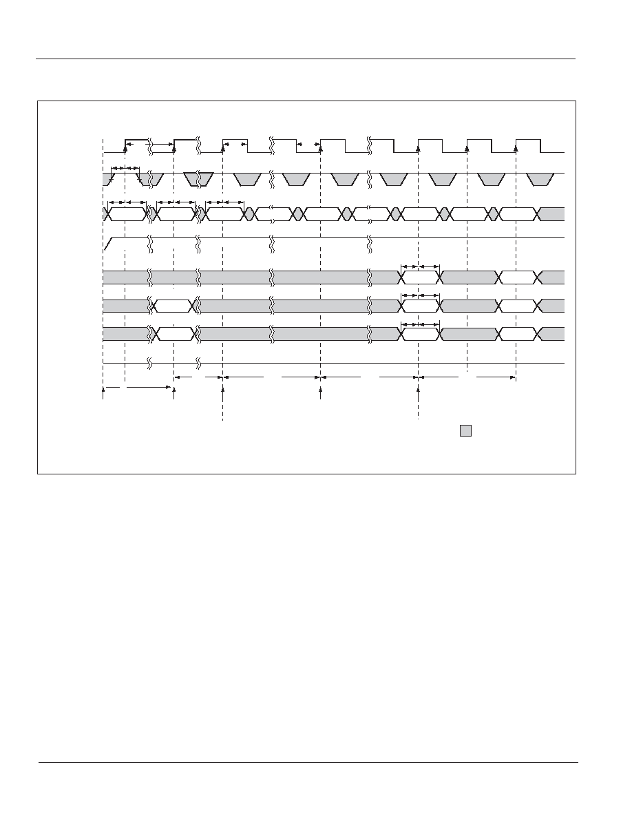
INITIALIZE AND LOAD MODE REGISTER
(1)
DON'T CARE
CLK
CKE
COMMAND
DQM/
DQML, DQMH
A0-A9, A11
A10
BA0, BA1
DQ
t
CH
t
CL
t
CK
t
CMH
t
CMS
t
CMH
t
CMS
t
CMH
t
CMS
t
CKS
t
CKH
T0 T1 Tn+1 To+1 Tp+1
Tp+2
Tp+3
t
MRD
t
RC
t
RC
t
RP
ROW
ROW
BANK
t
AS
t
AH
t
AS
t
AH
CODE
CODE
ALL BANKS
SINGLE BANK
ALL BANKS
AUTO
REFRESH
AUTO
REFRESH
Load MODE
REGISTER
T = 100µs Min.
Power-up: V
CC
and CLK stable
Precharge
all banks
AUTO REFRESH
Program MODE REGISTER
NOP
PRECHARGE NOP NOP
NOP
ACTIVE
T
(2, 3, 4)
AUTO REFRESH
CODE
t
AS
t
AH
Notes:
1. If
CS is High at clock High time, all commands applied are NOP.
2. The Mode register may be loaded prior to the Auto-Refresh cycles if desired.
3. JEDEC and PC100 specify three clocks.
4. Outputs are guaranteed High-Z after the command is issued.
Integrated Silicon Solution, Inc. -- www.issi.com --
1-800-379-4774
21
Rev. E
05/01/06
ISSI
Æ
IS42S81600B, IS42S16800B
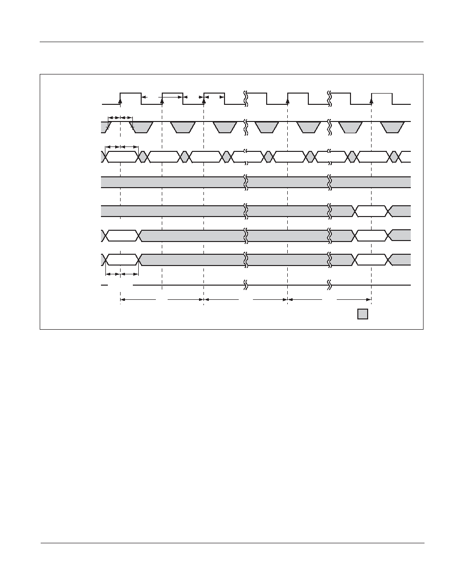
AUTO-REFRESH CYCLE
Notes:
1.
CAS latency = 2, 3
t
RP
t
RC
t
RC
DON'T CARE
CLK
CKE
COMMAND
DQM/
DQML, DQMH
A0-A9, A11
A10
BA0, BA1
DQ
t
AS
t
AH
t
CH
t
CL
t
CK
t
CMS
t
CMH
t
CKS
t
CKH
T0 T1 T2 Tn+1 To+1
ALL BANKS
SINGLE BANK
BANK
(s)
ROW
ROW
BANK
High-Z
PRECHARGE NOP
NOP
NOP ACTIVE
Auto
Refresh
Auto
Refresh
ISSI
Æ
22
Integrated Silicon Solution, Inc. -- www.issi.com --
1-800-379-4774
Rev. E
05/01/06
IS42S81600B, IS42S16800B
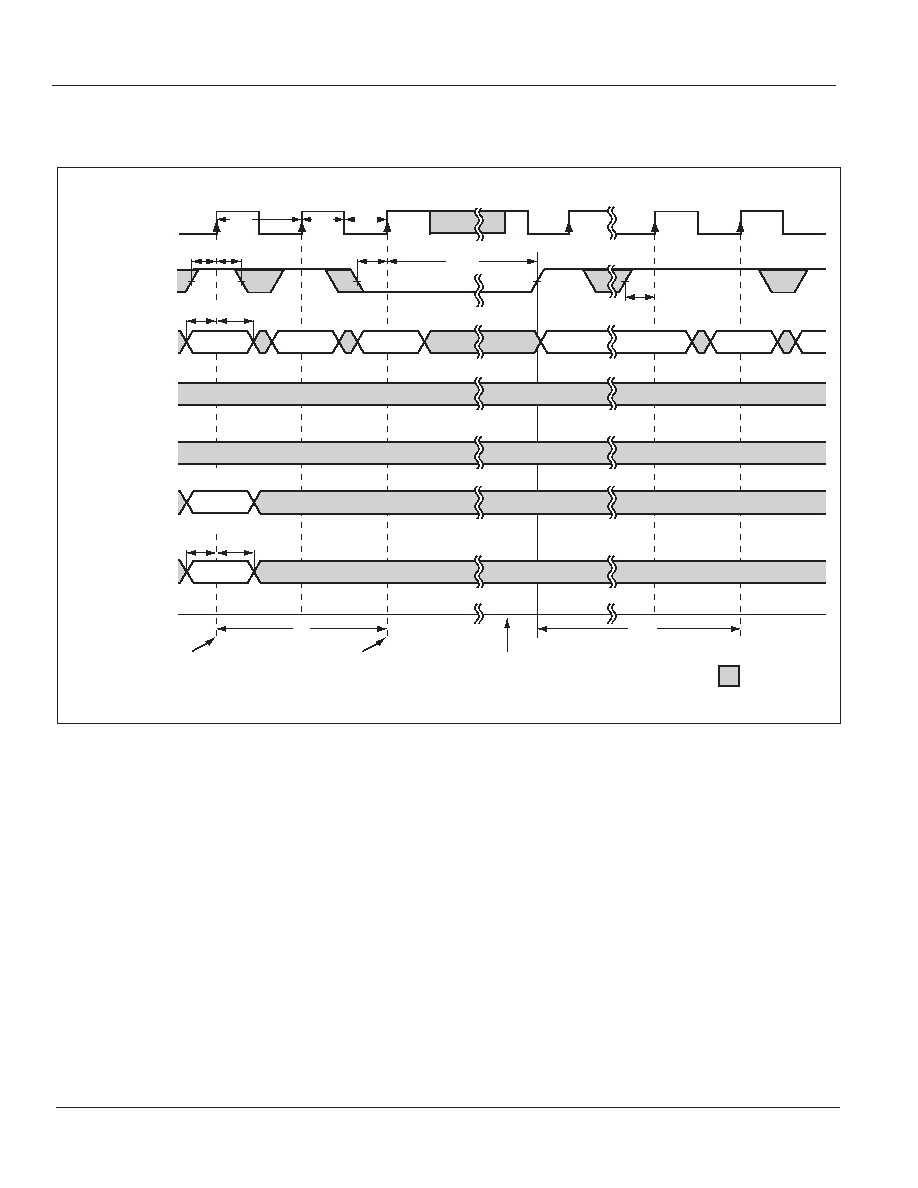
SELF-REFRESH CYCLE
CLK
CKE
COMMAND
DQM/
DQML, DQMH
A0-A9, A11
A10
BA0, BA1
DQ
t
AS
t
AH
BANK
t
CL
t
CH
t
CK
t
CMS
t
CMH
t
CKS
t
CKH
ALL BANKS
SINGLE BANK
t
CKS
Precharge all
active banks
CLK stable prior to exiting
self refresh mode
Enter self
refresh mode
Exit self refresh mode
(Restart refresh time base)
T0 T1 T2
Tn+1
To+1
To+2
High-Z
Auto
Refresh
Auto
Refresh
PRECHARGE NOP
NOP NOP
t
CKS
t
RAS
t
RP
t
SRX
DON'T CARE
Integrated Silicon Solution, Inc. -- www.issi.com --
1-800-379-4774
23
Rev. E
05/01/06
ISSI
Æ
IS42S81600B, IS42S16800B
REGISTER DEFINITION
Mode Register
The mode register is used to define the specific mode of
operation of the SDRAM. This definition includes the
selection of a burst length, a burst type, a CAS latency, an
operating mode and a write burst mode, as shown in MODE
REGISTER DEFINITION.
The mode register is programmed via the LOAD MODE
REGISTER command and will retain the stored information
until it is programmed again or the device loses power.
Mode register bits M0-M2 specify the burst length, M3
specifies the type of burst (sequential or interleaved), M4- M6
specify the CAS latency, M7 and M8 specify the operating
mode, M9 specifies the WRITE burst mode, and M10 and
M11 are reserved for future use.
The mode register must be loaded when all banks are idle,
and the controller must wait the specified time before
initiating the subsequent operation. Violating either of these
requirements will result in unspecified operation.
MODE REGISTER DEFINITION
Latency Mode
M6 M5 M4
CAS
Latency
0 0 0
Reserved
0 0 1
Reserved
0 1 0
2
0 1 1
3
1 0 0
Reserved
1 0 1
Reserved
1 1 0
Reserved
1 1 1
Reserved
1. To ensure compatibility with future devices,
should program BA1, BA0, A11, A10 = "0"
Write Burst Mode
M9
Mode
0
Programmed Burst Length
1
Single Location Access
Operating Mode
M8 M7 M6-M0 Mode
0 0 Defined Standard
Operation
-- --
--
All Other States Reserved
Burst Type
M3
Type
0
Sequential
1 Interleaved
Burst Length
M2 M1 M0
M3=0
M3=1
0
0
0 1 1
0
0
1 2 2
0
1
0 4 4
0
1
1 8 8
1 0 0
Reserved Reserved
1 0 1
Reserved Reserved
1 1 0
Reserved Reserved
1 1 1
Full
Page Reserved
Reserved
Address Bus
Mode Register (Mx)
(1)
BA1 BA0
A11 A10
A9
A8 A7 A6 A5 A4 A3 A2 A1 A0

ISSI
Æ
24
Integrated Silicon Solution, Inc. -- www.issi.com --
1-800-379-4774
Rev. E
05/01/06
IS42S81600B, IS42S16800B
BURST DEFINITION
Burst
Starting Column
Order of Accesses Within a Burst
Length
Address
Type = Sequential
Type = Interleaved
A 0
2
0
0-1
0-1
1
1-0
1-0
A 1
A 0
0
0
0-1-2-3
0-1-2-3
4
0
1
1-2-3-0
1-0-3-2
1
0
2-3-0-1
2-3-0-1
1
1
3-0-1-2
3-2-1-0
A 2
A 1
A 0
0
0
0
0-1-2-3-4-5-6-7
0-1-2-3-4-5-6-7
0
0
1
1-2-3-4-5-6-7-0
1-0-3-2-5-4-7-6
0
1
0
2-3-4-5-6-7-0-1
2-3-0-1-6-7-4-5
8
0
1
1
3-4-5-6-7-0-1-2
3-2-1-0-7-6-5-4
1
0
0
4-5-6-7-0-1-2-3
4-5-6-7-0-1-2-3
1
0
1
5-6-7-0-1-2-3-4
5-4-7-6-1-0-3-2
1
1
0
6-7-0-1-2-3-4-5
6-7-4-5-2-3-0-1
1
1
1
7-0-1-2-3-4-5-6
7-6-5-4-3-2-1-0
Full
n = A0-A7
Cn, Cn + 1, Cn + 2
Not Supported
Page
Cn + 3, Cn + 4...
(y)
(location 0-y)
...Cn - 1,
Cn...
BURST LENGTH
Read and write accesses to the SDRAM are burst oriented,
with the burst length being programmable, as shown in
MODE REGISTER DEFINITION. The burst length deter-
mines the maximum number of column locations that can
be accessed for a given READ or WRITE command. Burst
lengths of 1, 2, 4 or 8 locations are available for both the
sequential and the interleaved burst types, and a full-page
burst is available for the sequential type. The full-page burst
is used in conjunction with the BURST TERMINATE com-
mand to generate arbitrary burst lengths.
Reserved states should not be used, as unknown operation
or incompatibility with future versions may result.
When a READ or WRITE command is issued, a block of
columns equal to the burst length is effectively selected. All
accesses for that burst take place within this block, mean-
ing that the burst will wrap within the block if a boundary is
reached. The block is uniquely selected by A1-A8 (x16)
when the burst length is set to two; by A2-A8 (x16) when the
burst length is set to four; and by A3-A8 (x16) when the burst
length is set to eight. The remaining (least significant)
address bit(s) is (are) used to select the starting location
within the block. Full-page bursts wrap within the page if the
boundary is reached.
Burst Type
Accesses within a given burst may be programmed to be
either sequential or interleaved; this is referred to as the
burst type and is selected via bit M3.
The ordering of accesses within a burst is determined by the
burst length, the burst type and the starting column address,
as shown in BURST DEFINITION table.
Integrated Silicon Solution, Inc. -- www.issi.com --
1-800-379-4774
25
Rev. E
05/01/06
ISSI
Æ
IS42S81600B, IS42S16800B
DON'T CARE
UNDEFINED
CLK
COMMAND
DQ
READ NOP NOP NOP
CAS Latency - 3
t
AC
t
OH
D
OUT
T0 T1 T2 T3 T4
t
LZ
CLK
COMMAND
DQ
READ NOP NOP
CAS Latency - 2
t
AC
t
OH
D
OUT
T0 T1 T2 T3
t
LZ
CAS LATENCY
CAS Latency
The CAS latency is the delay, in clock cycles, between the
registration of a READ command and the availability of the
first piece of output data. The latency can be set to two or
three clocks.
If a READ command is registered at clock edge n, and the
latency is
m clocks, the data will be available by clock edge
n + m. The DQs will start driving as a result of the clock edge
one cycle earlier
(n + m - 1), and provided that the relevant
access times are met, the data will be valid by clock edge
n + m. For example, assuming that the clock cycle time is
such that all relevant access times are met, if a READ
command is registered at T0 and the latency is programmed
to two clocks, the DQs will start driving after T1 and the data
will be valid by T2, as shown in CAS Latency diagrams. The
Allowable Operating Frequency table indicates the operat-
ing frequencies at which each CAS latency setting can be
used.
Reserved states should not be used as unknown operation or
incompatibility with future versions may result.
CAS Latency
Allowable Operating Frequency (MHz)
Speed
CAS Latency = 2
CAS Latency = 3
-6
--
167
-7
--
143
-75E
133
--
Operating Mode
The normal operating mode is selected by setting M7 and M8
to zero; the other combinations of values for M7 and M8 are
reserved for future use and/or test modes. The programmed
burst length applies to both READ and WRITE bursts.
Test modes and reserved states should not be used
because unknown operation or incompatibility with future
versions may result.
Write Burst Mode
When M9 = 0, the burst length programmed via M0-M2
applies to both READ and WRITE bursts; when M9 = 1, the
programmed burst length applies to READ bursts, but write
accesses are single-location (nonburst) accesses.
ISSI
Æ
26
Integrated Silicon Solution, Inc. -- www.issi.com --
1-800-379-4774
Rev. E
05/01/06
IS42S81600B, IS42S16800B
CLK
CKE
ROW ADDRESS
BANK ADDRESS
CS
RAS
CAS
WE
A0-A11
BA0, BA1
HIGH
ACTIVATING SPECIFIC ROW WITHIN SPE-
CIFIC BANK
DON'T CARE
CLK
COMMAND
ACTIVE NOP NOP
t
RCD
T0 T1 T2 T3 T4
READ or
WRITE
CHIP OPERATION
BANK/ROW ACTIVATION
Before any READ or WRITE commands can be issued to a
bank within the SDRAM, a row in that bank must be "opened."
This is accomplished via the ACTIVE command, which
selects both the bank and the row to be activated (see
Activating Specific Row Within Specific Bank).
After opening a row (issuing an ACTIVE command), a
READ or WRITE command may be issued to that row,
subject to the t
RCD
specification. Minimum t
RCD
should be
divided by the clock period and rounded up to the next whole
number to determine the earliest clock edge after the
ACTIVE command on which a READ or WRITE command
can be entered. For example, a t
RCD
specification of 18ns
with a 125 MHz clock (8ns period) results in 2.25 clocks,
rounded to 3. This is reflected in the following example,
which covers any case where 2 < [t
RCD
(MIN)/t
CK
]
3. (The
same procedure is used to convert other specification limits
from time units to clock cycles).
A subsequent ACTIVE command to a different row in the
same bank can only be issued after the previous active row
has been "closed" (precharged). The minimum time interval
between successive ACTIVE commands to the same bank
is defined by t
RC
.
A subsequent ACTIVE command to another bank can be
issued while the first bank is being accessed, which results
in a reduction of total row-access overhead. The minimum
time interval between successive ACTIVE commands to
different banks is defined by t
RRD
.
EXAMPLE: MEETING TRCD (MIN) WHEN 2
<<
<<
< [TRCD (MIN)/TCK] 3
Integrated Silicon Solution, Inc. -- www.issi.com --
1-800-379-4774
27
Rev. E
05/01/06
ISSI
Æ
IS42S81600B, IS42S16800B
CLK
CKE
HIGH
COLUMN ADDRESS
AUTO PRECHARGE
NO PRECHARGE
CS
RAS
CAS
WE
A0-A9
A10
BA0, BA1
BANK ADDRESS
A11
READ COMMAND
READS
READ bursts are initiated with a READ command, as shown
in the READ COMMAND diagram.
The starting column and bank addresses are provided with the
READ command, and auto precharge is either enabled or
disabled for that burst access. If auto precharge is enabled, the
row being accessed is precharged at the completion of the
burst. For the generic READ commands used in the following
illustrations, auto precharge is disabled.
During READ bursts, the valid data-out element from the
starting column address will be available following the CAS
latency after the READ command. Each subsequent data-
out element will be valid by the next positive clock edge. The
CAS Latency diagram shows general timing
for each possible CAS latency setting.
Upon completion of a burst, assuming no other commands
have been initiated, the DQs will go High-Z. A full-page burst
will continue until terminated. (At the end of the page, it will
wrap to column 0 and continue.)
Data from any READ burst may be truncated with a subse-
quent READ command, and data from a fixed-length READ
burst may be immediately followed by data from a READ
command. In either case, a continuous flow of data can be
maintained. The first data element from the new burst follows
either the last element of a completed burst or the last desired
data element of a longer burst which is being truncated.
The new READ command should be issued
x cycles before
the clock edge at which the last desired data element is
valid, where
x equals the CAS latency minus one. This is
shown in Consecutive READ Bursts for CAS latencies of
two and three; data element
n + 3 is either the last of a burst
of four or the last desired of a longer burst. The 128Mb
SDRAM uses a pipelined architecture and therefore does
not require the
2n rule associated with a prefetch architec-
ture. A READ command can be initiated on any clock cycle
following a previous READ command. Full-speed random
read accesses can be performed to the same bank, as shown
in Random READ Accesses, or each subsequent READ
may be performed to a different bank.
Data from any READ burst may be truncated with a
subsequent WRITE command, and data from a fixed-length
READ burst may be immediately followed by data from a
WRITE command (subject to bus turnaround limitations).
The WRITE burst may be initiated on the clock edge
immediately following the last (or last desired) data element
from the READ burst, provided that I/O contention can be
avoided. In a given system design, there may be a possi-
bility that the device driving the input data will go Low-Z
before the SDRAM DQs go High-Z. In this case, at least a
single-cycle delay should occur between the last read data
and the WRITE command.
The DQM input is used to avoid I/O contention, as shown
in Figures RW1 and RW2. The DQM signal must be
asserted (HIGH) at least three clocks prior to the WRITE
command (DQM latency is two clocks for output buffers) to
suppress data-out from the READ. Once the WRITE com-
mand is registered, the DQs will go High-Z (or remain High-
Z), regardless of the state of the DQM signal, provided the
DQM was active on the clock just prior to the WRITE
command that truncated the READ command. If not, the
second WRITE will be an invalid WRITE. For example, if
DQM was LOW during T4 in Figure RW2, then the WRITEs
at T5 and T7 would be valid, while the WRITE at T6 would
be invalid.
The DQM signal must be de-asserted prior to the WRITE
command (DQM latency is zero clocks for input buffers) to
ensure that the written data is not masked.
A fixed-length READ burst may be followed by, or truncated
with, a PRECHARGE command to the same bank (provided
that auto precharge was not activated), and a full-page burst
may be truncated with a PRECHARGE command to the
same bank. The PRECHARGE command should be issued
x cycles before the clock edge at which the last desired data
element is valid, where
x equals the CAS latency minus one.
This is shown in the READ to PRECHARGE diagram for each
Note: A9 is "Don't Care" for x16.

ISSI
Æ
28
Integrated Silicon Solution, Inc. -- www.issi.com --
1-800-379-4774
Rev. E
05/01/06
IS42S81600B, IS42S16800B
possible CAS latency; data element
n + 3 is either the last of
a burst of four or the last desired of a longer burst. Following
the PRECHARGE command, a subsequent command to the
same bank cannot be issued until t
RP
is met. Note that part
of the row precharge time is hidden during the access of the
last data element(s).
In the case of a fixed-length burst being executed to
completion, a PRECHARGE command issued at the opti-
mum time (as described above) provides the same opera-
tion that would result from the same fixed-length burst with
auto precharge. The disadvantage of the PRECHARGE
command is that it requires that the command and address
buses be available at the appropriate time to issue the
command; the advantage of the PRECHARGE command is
that it can be used to truncate fixed-length or full-page
bursts.
Full-page READ bursts can be truncated with the BURST
TERMINATE command, and fixed-length READ bursts
may be truncated with a BURST TERMINATE command,
provided that auto precharge was not activated. The BURST
TERMINATE command should be issued
x cycles before
the clock edge at which the last desired data element is
valid, where
x equals the CAS latency minus one. This is
shown in the READ Burst Termination diagram for each
possible CAS latency; data element
n + 3 is the last desired
data element of a longer burst.
Integrated Silicon Solution, Inc. -- www.issi.com --
1-800-379-4774
29
Rev. E
05/01/06
ISSI
Æ
IS42S81600B, IS42S16800B
DON'T CARE
CLK
DQM
COMMAND
ADDRESS
DQ
T0 T1 T2 T3 T4 T5
READ NOP NOP NOP NOP WRITE
BANK,
COL n
BANK,
COL b
D
OUT
n
D
IN
b
t
DS
t
HZ
CAS Latency - 3
RW1 - READ to WRITE
RW2 - READ to WRITE
DON'T CARE
CLK
DQM
COMMAND
ADDRESS
DQ
T0 T1 T2 T3 T4 T5 T6
READ NOP NOP NOP NOP NOP WRITE
BANK,
COL n
D
IN
b
t
DS
t
HZ
BANK,
COL b
CAS Latency - 2
D
OUT
n
D
OUT
n+1
D
OUT
n+2
ISSI
Æ
30
Integrated Silicon Solution, Inc. -- www.issi.com --
1-800-379-4774
Rev. E
05/01/06
IS42S81600B, IS42S16800B
DON'T CARE
CLK
COMMAND
ADDRESS
DQ
T0 T1 T2 T3 T4 T5 T6
READ NOP NOP NOP READ NOP NOP
D
OUT
n
D
OUT
n+1
D
OUT
n+2
D
OUT
n+3
D
OUT
b
BANK,
COL n
BANK,
COL b
CAS Latency - 2
DON'T CARE
CLK
COMMAND
ADDRESS
DQ
T0 T1 T2 T3 T4 T5 T6 T7
READ NOP NOP NOP READ NOP NOP NOP
D
OUT
n
D
OUT
n+1
D
OUT
n+2
D
OUT
n+3
D
OUT
b
BANK,
COL n
BANK,
COL b
CAS Latency - 3
CONSECUTIVE READ BURSTS
Integrated Silicon Solution, Inc. -- www.issi.com --
1-800-379-4774
31
Rev. E
05/01/06
ISSI
Æ
IS42S81600B, IS42S16800B
DON'T CARE
CLK
COMMAND
ADDRESS
DQ
T0 T1 T2 T3 T4 T5
READ
READ
READ
READ NOP NOP
D
OUT
n
D
OUT
b
D
OUT
m
D
OUT
x
BANK,
COL n
BANK,
COL b
CAS Latency - 2
BANK,
COL m
BANK,
COL x
DON'T CARE
CLK
COMMAND
ADDRESS
DQ
T0 T1 T2 T3 T4 T5 T6
READ
READ
READ
READ NOP NOP NOP
D
OUT
n
D
OUT
b
D
OUT
m
D
OUT
x
BANK,
COL n
BANK,
COL b
CAS Latency - 3
BANK,
COL m
BANK,
COL x
RANDOM READ ACCESSES
ISSI
Æ
32
Integrated Silicon Solution, Inc. -- www.issi.com --
1-800-379-4774
Rev. E
05/01/06
IS42S81600B, IS42S16800B
DON'T CARE
CLK
COMMAND
ADDRESS
DQ
T0 T1 T2 T3 T4 T5 T6
READ NOP NOP NOP
NOP NOP
D
OUT
n
D
OUT
n+1
D
OUT
n+2
D
OUT
n+3
BANK a,
COL n
CAS Latency - 2
x = 1 cycle
BURST
TERMINATE
DON'T CARE
CLK
COMMAND
ADDRESS
DQ
T0 T1 T2 T3 T4 T5 T6 T7
READ NOP NOP NOP
NOP NOP NOP
D
OUT
n
D
OUT
n+1
D
OUT
n+2
D
OUT
n+3
BANK,
COL n
CAS Latency - 3
x = 2 cycles
BURST
TERMINATE
READ BURST TERMINATION
Integrated Silicon Solution, Inc. -- www.issi.com --
1-800-379-4774
33
Rev. E
05/01/06
ISSI
Æ
IS42S81600B, IS42S16800B
ALTERNATING BANK READ ACCESSES
BANK 0
BANK 3
BANK 3
BANK 0
DON'T CARE
CLK
CKE
COMMAND
DQM/
DQML, DQMH
A0-A9, A11
A10
BA0, BA1
DQ
t
CMS
t
CMH
t
AS
t
AH
t
AS
t
AH
t
AS
t
AH
t
RCD
- BANK 0
CAS Latency - BANK 0
t
RCD
- BANK 0
t
RAS
- BANK 0
t
RC
- BANK 0
t
CH
t
CL
t
CK
t
CMS
t
CMH
t
CKS
t
CKH
ACTIVE NOP READ NOP ACTIVE NOP READ NOP ACTIVE
ROW
ROW
BANK 0
ROW ROW
t
RRD
t
RCD
- BANK 3
t
RP
- BANK 0
COLUMN m
(2)
ROW COLUMN
b
(2)
ROW
ENABLE AUTO PRECHARGE
ENABLE AUTO PRECHARGE
T0 T1 T2 T3 T4 T5 T6 T7 T8
t
AC
t
OH
t
OH
t
OH
t
OH
t
OH
D
OUT
m
D
OUT
m+
1
D
OUT
m+
2
D
OUT
m+
3
D
OUT
b
t
AC
t
AC
t
AC
t
AC
t
AC
t
LZ
CAS Latency - BANK 3
Notes:
1)
CAS latency = 2, Burst Length = 4
2) X16: A9 and A11 = "Don't Care"
X8: A11 = "Don't Care"
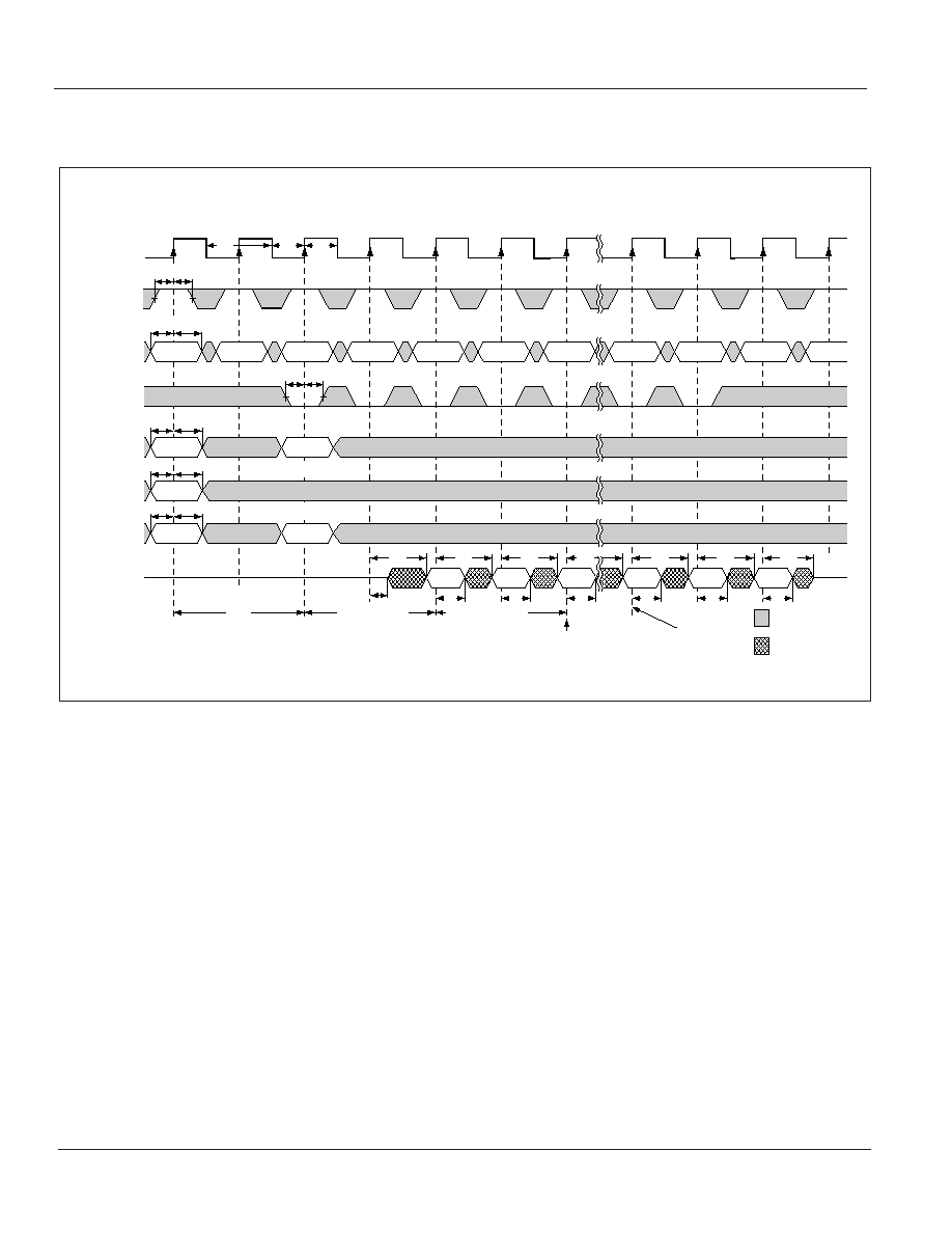
ISSI
Æ
34
Integrated Silicon Solution, Inc. -- www.issi.com --
1-800-379-4774
Rev. E
05/01/06
IS42S81600B, IS42S16800B
READ - FULL-PAGE BURST
DON'T CARE
UNDEFINED
CLK
CKE
COMMAND
DQM/
DQML, DQMH
A0-A9, A11
A10
BA0, BA1
DQ
t
CMS
t
CMH
ACTIVE NOP READ NOP NOP NOP NOP NOP
BURST TERM
NOP
NOP
t
AS
t
AH
t
AS
t
AH
t
AS
t
AH
ROW
ROW
BANK
COLUMN m
(2)
t
CH
t
CL
t
CK
t
CMS
t
CMH
t
CKS
t
CKH
BANK
t
RCD
CAS Latency
t
AC
t
AC
t
AC
t
AC
t
AC
t
HZ
t
LZ
t
AC
t
OH
t
OH
t
OH
t
OH
t
OH
t
OH
D
OUT
m
D
OUT
m+
1
D
OUT
m+
2
D
OUT
m-
1
D
OUT
m
D
OUT
m+
1
each row (x4) has
1,024 locations
Full page
completion
Full-page burst not self-terminating.
Use BURST TERMINATE command.
T0 T1 T2 T3 T4 T5 T6 Tn+1
Tn+2
Tn+3
Tn+4
Notes:
1)
CAS latency = 2, Burst Length = Full Page
2) X16: A9 and A11 = "Don't Care"
X8: A11 = "Don't Care"
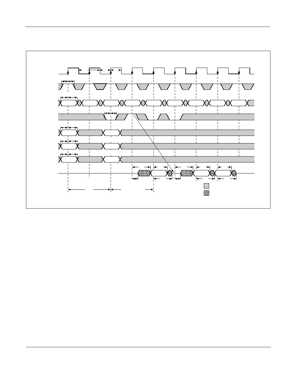
Integrated Silicon Solution, Inc. -- www.issi.com --
1-800-379-4774
35
Rev. E
05/01/06
ISSI
Æ
IS42S81600B, IS42S16800B
READ - DQM OPERATION
DON'T CARE
UNDEFINED
CLK
CKE
COMMAND
DQM/
DQML, DQMH
A0-A9, A11
A10
BA0, BA1
DQ
t
CMS
t
CMH
ACTIVE
NOP READ NOP NOP NOP NOP NOP NOP
t
AS
t
AH
t
AS
t
AH
t
AS
t
AH
ENABLE AUTO PRECHARGE
DISABLE AUTO PRECHARGE
ROW
ROW
BANK
t
RCD
CAS Latency
D
OUT
m
D
OUT
m+
2
D
OUT
m+
3
COLUMN m
(2)
BANK
t
CH
t
CL
t
CK
t
CMS
t
CMH
t
CKS
t
CKH
t
OH
t
OH
t
OH
t
AC
t
AC
t
AC
t
HZ
t
HZ
t
LZ
t
LZ
T0 T1 T2 T3 T4 T5 T6 T7 T8
Notes:
1)
CAS latency = 2, Burst Length = 4
2) X16: A9 and A11 = "Don't Care"
X8: A11 = "Don't Care"
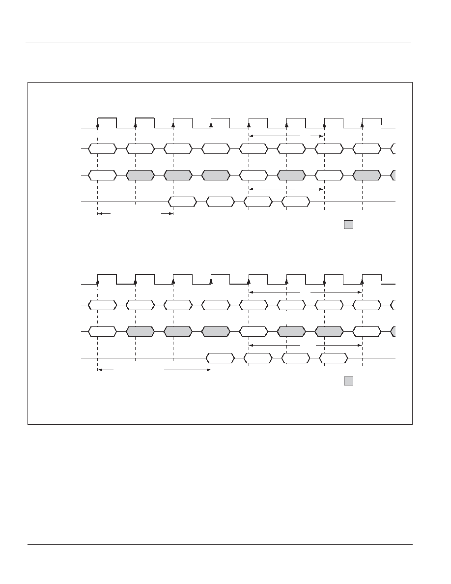
ISSI
Æ
36
Integrated Silicon Solution, Inc. -- www.issi.com --
1-800-379-4774
Rev. E
05/01/06
IS42S81600B, IS42S16800B
DON'T CARE
CLK
COMMAND
ADDRESS
DQ
T0 T1 T2 T3 T4 T5 T6 T7
READ NOP NOP NOP
NOP
ACTIVE
NOP
D
OUT
n
D
OUT
n+1
D
OUT
n+2
D
OUT
n+3
BANK a,
COL n
BANK a,
ROW
BANK
(a or all)
CAS Latency - 2
t
RP
PRECHARGE
t
RQL
High-Z
DON'T CARE
CLK
COMMAND
ADDRESS
DQ
T0 T1 T2 T3 T4 T5 T6 T7
READ NOP NOP NOP
NOP NOP
ACTIVE
D
OUT
n
D
OUT
n+1
D
OUT
n+2
D
OUT
n+3
BANK,
COL n
BANK,
COL b
CAS Latency - 3
t
RP
t
RQL
BANK a,
ROW
PRECHARGE
High-Z
READ to PRECHARGE
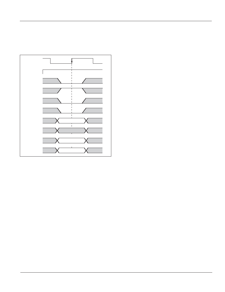
Integrated Silicon Solution, Inc. -- www.issi.com --
1-800-379-4774
37
Rev. E
05/01/06
ISSI
Æ
IS42S81600B, IS42S16800B
CLK
CKE
HIGH
COLUMN ADDRESS
AUTO PRECHARGE
BANK ADDRESS
CS
RAS
CAS
WE
A0-A9
A10
BA0, BA1
NO PRECHARGE
A11
WRITE COMMAND
The starting column and bank addresses are provided with
the WRITE command, and auto precharge is either enabled
or disabled for that access. If auto precharge is enabled, the
row being accessed is precharged at the completion of the
burst. For the generic WRITE commands used in the
following illustrations, auto precharge is disabled.
During WRITE bursts, the first valid data-in element will be
registered coincident with the WRITE command. Subsequent
data elements will be registered on each successive positive
clock edge. Upon completion of a fixed-length burst, assum-
ing no other commands have been initiated, the DQs will
remain High-Z and any additional input data will be ignored
(see WRITE Burst). A full-page burst will continue until
terminated. (At the end of the page, it will wrap to column 0
and continue.)
Data for any WRITE burst may be truncated with a subse-
quent WRITE command, and data for a fixed-length WRITE
burst may be immediately followed by data for a WRITE
command. The new WRITE command can be issued on any
clock following the previous WRITE command, and the data
provided coincident with the new command applies to the new
command.
An example is shown in WRITE to WRITE diagram. Data
n
+ 1 is either the last of a burst of two or the last desired of
a longer burst. The 128Mb SDRAM uses a pipelined
architecture and therefore does not require the
2n rule
associated with a prefetch architecture. A WRITE command
can be initiated on any clock cycle following a previous
WRITE command. Full-speed random write accesses within
a page can be performed to the same bank, as shown in
Random WRITE Cycles, or each subsequent WRITE may
be performed to a different bank.
Data for any WRITE burst may be truncated with a subse-
quent READ command, and data for a fixed-length WRITE
burst may be immediately followed by a subsequent READ
command. Once the READ com mand is registered, the
data inputs will be ignored, and WRITEs will not be ex-
ecuted. An example is shown in WRITE to READ. Data
n +
1 is either the last of a burst of two or the last desired of a
longer burst.
Data for a fixed-length WRITE burst may be followed by, or
truncated with, a PRECHARGE command to the same bank
(provided that auto precharge was not activated), and a full-
page WRITE burst may be truncated with a PRECHARGE
command to the same bank. The PRECHARGE command
should be issued t
DPL
after the clock edge at which the last
desired input data element is registered. The auto precharge
mode requires a t
DPL
of at least one clock plus time,
regardless of frequency. In addition, when truncating a
WRITE burst, the DQM signal must be used to mask input
data for the clock edge prior to, and the clock edge coincident
with, the PRECHARGE command. An example is shown in the
WRITE to PRECHARGE diagram. Data
n+1 is either the last
of a burst of two or the last desired of a longer burst. Following
the PRECHARGE command, a subsequent command to the
same bank cannot be issued until t
RP
is met.
In the case of a fixed-length burst being executed to comple-
tion, a PRECHARGE command issued at the optimum time (as
described above) provides the same operation that would result
from the same fixed-length burst with auto precharge. The
disadvantage of the PRECHARGE command is that it requires
that the command and address buses be available at the
appropriate time to issue the command; the advantage of the
PRECHARGE command is that it can be used to truncate
fixed-length or full-page bursts.
Fixed-length or full-page WRITE bursts can be truncated
with the BURST TERMINATE command. When truncating
a WRITE burst, the input data applied coincident with the
BURST TERMINATE command will be ignored. The last
data written (provided that DQM is LOW at that time) will be
the input data applied one clock previous to the BURST
TERMINATE command. This is shown in WRITE Burst
Termination, where data
n is the last desired data element
of a longer burst.
WRITES
WRITE bursts are initiated with a WRITE command, as
shown in WRITE Command diagram.
Note: A9 is "Don't Care" for x16.
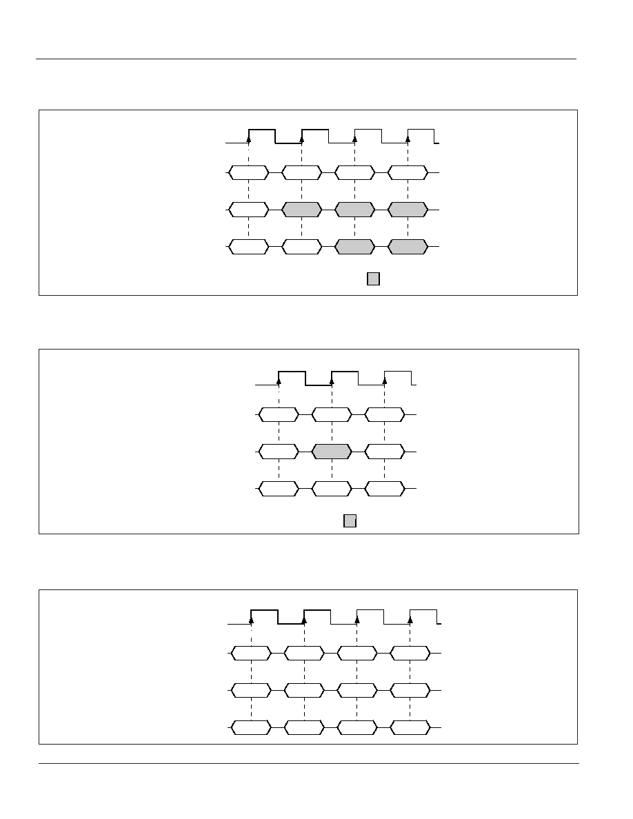
ISSI
Æ
38
Integrated Silicon Solution, Inc. -- www.issi.com --
1-800-379-4774
Rev. E
05/01/06
IS42S81600B, IS42S16800B
CLK
COMMAND
ADDRESS
DQ
T0 T1 T2 T3
WRITE
NOP
NOP
NOP
D
IN
n
D
IN
n+1
BANK,
COL n
DON'T CARE
CLK
COMMAND
ADDRESS
DQ
T0 T1 T2
WRITE
NOP
WRITE
D
IN
n
D
IN
n+1
D
IN
b
BANK,
COL n
BANK,
COL b
DON'T CARE
WRITE BURST
WRITE TO WRITE
CLK
COMMAND
ADDRESS
DQ
T0 T1 T2 T3
WRITE
WRITE
WRITE
WRITE
D
IN
n
D
IN
b
D
IN
m
D
IN
x
BANK,
COL n
BANK,
COL b
BANK,
COL m
BANK,
COL x
RANDOM WRITE CYCLES
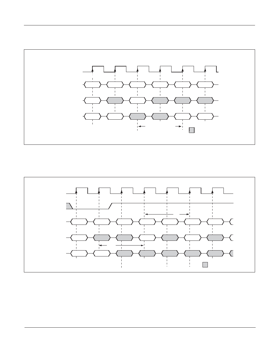
Integrated Silicon Solution, Inc. -- www.issi.com --
1-800-379-4774
39
Rev. E
05/01/06
ISSI
Æ
IS42S81600B, IS42S16800B
DON'T CARE
CLK
COMMAND
ADDRESS
DQ
T0 T1 T2 T3 T4 T5
WRITE
NOP
READ
NOP NOP NOP
D
IN
n
D
IN
n+1
D
OUT
b
D
OUT
b+1
BANK,
COL n
BANK,
COL b
CAS Latency - 2
WRITE to READ
WP1 - WRITE to PRECHARGE
DON'T CARE
CLK
DQM
COMMAND
ADDRESS
DQ
T0 T1 T2 T3 T4 T5 T6
WRITE NOP NOP
NOP ACTIVE NOP
BANK a,
COL n
BANK a,
ROW
BANK
(a or all)
t
DPL
t
RP
PRECHARGE
D
IN
n
D
IN
n+1
D
IN
n+2
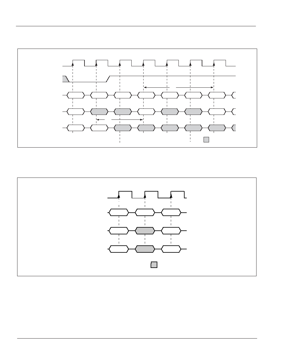
ISSI
Æ
40
Integrated Silicon Solution, Inc. -- www.issi.com --
1-800-379-4774
Rev. E
05/01/06
IS42S81600B, IS42S16800B
CLK
COMMAND
ADDRESS
DQ
T0 T1 T2
WRITE
D
IN
n
(DATA)
BANK,
COL n
DON'T CARE
(ADDRESS)
BURST
TERMINATE
NEXT
COMMAND
WRITE Burst Termination
DON'T CARE
CLK
DQM
COMMAND
ADDRESS
DQ
T0 T1 T2 T3 T4 T5 T6
WRITE NOP NOP
NOP NOP ACTIVE
BANK a,
COL n
BANK a,
ROW
BANK
(a or all)
t
DPL
t
RP
PRECHARGE
D
IN
n
D
IN
n+1
WP2 - WRITE to PRECHARGE

Integrated Silicon Solution, Inc. -- www.issi.com --
1-800-379-4774
41
Rev. E
05/01/06
ISSI
Æ
IS42S81600B, IS42S16800B
DON'T CARE
CLK
CKE
COMMAND
DQM/DQML
DQMH
A0-A9, A11
A10
BA0, BA1
DQ
t
CMS
t
CMH
ACTIVE NOP WRITE
NOP NOP NOP NOP
BURST TERM
NOP
t
AS
t
AH
t
AS
t
AH
t
AS
t
AH
t
DS
t
DH
t
DS
t
DH
t
DS
t
DH
ROW
ROW
BANK
t
RCD
D
IN
m
D
IN
m+
1
D
IN
m+
2
D
IN
m+
3
D
IN
m-
1
COLUMN m
(2)
t
CH
t
CL
t
CK
t
DS
t
DH
t
DS
t
DH
t
DS
t
DH
t
CMS
t
CMH
t
CKS
t
CKH
BANK
Full page completed
T0 T1 T2 T3 T4 T5 Tn+1
Tn+2
WRITE - FULL PAGE BURST
Notes:
1) Burst Length = Full Page
2) X16: A9 and A11 = "Don't Care"
X8: A11 = "Don't Care"
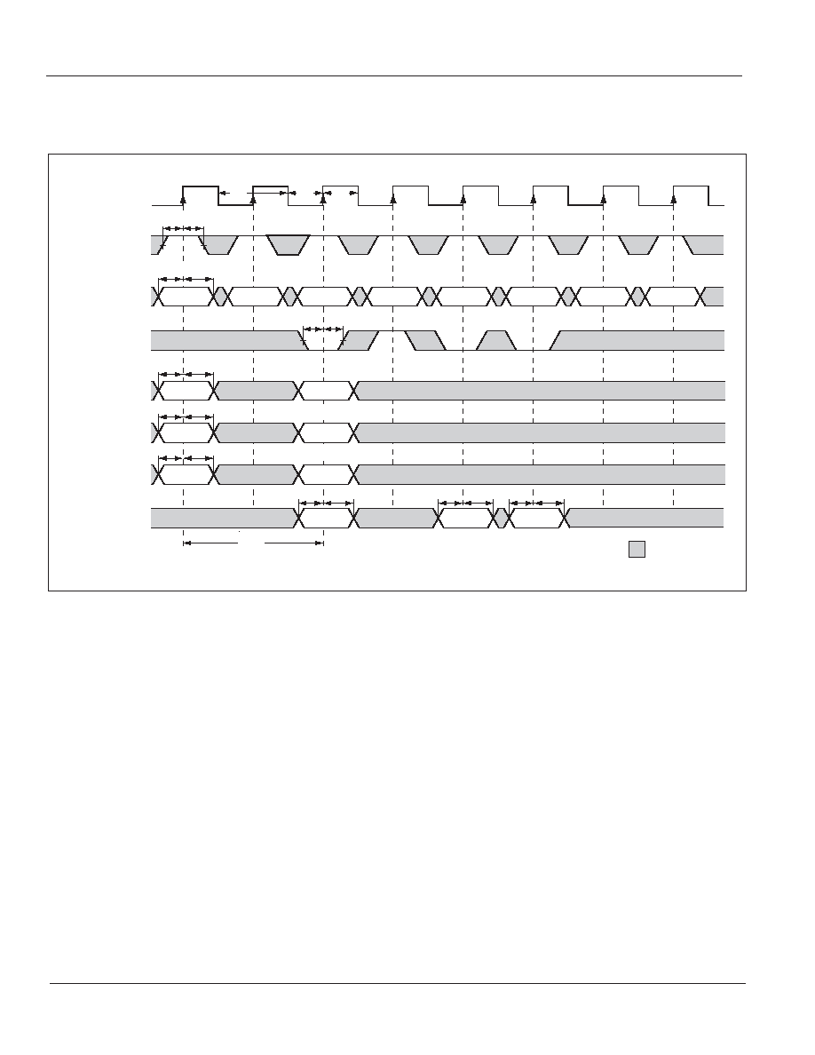
ISSI
Æ
42
Integrated Silicon Solution, Inc. -- www.issi.com --
1-800-379-4774
Rev. E
05/01/06
IS42S81600B, IS42S16800B
DON'T CARE
CLK
CKE
COMMAND
DQM/DQML
DQMH
A0-A9, A11
A10
BA0, BA1
DQ
t
CMS
t
CMH
ACTIVE
NOP WRITE
NOP NOP NOP NOP NOP
t
AS
t
AH
t
AS
t
AH
t
AS
t
AH
t
DS
t
DH
t
DS
t
DH
t
DS
t
DH
ENABLE AUTO PRECHARGE
DISABLE AUTO PRECHARGE
ROW
ROW
BANK
t
RCD
D
IN
m
D
IN
m+
2
D
IN
m+
3
COLUMN m
(2)
BANK
t
CH
t
CL
t
CK
t
CMS
t
CMH
t
CKS
t
CKH
T0 T1 T2 T3 T4 T5 T6 T7
WRITE - DQM OPERATION
Notes:
1) Burst Length = 4
2) X16: A9 and A11 = "Don't Care"
X8: A11 = "Don't Care"
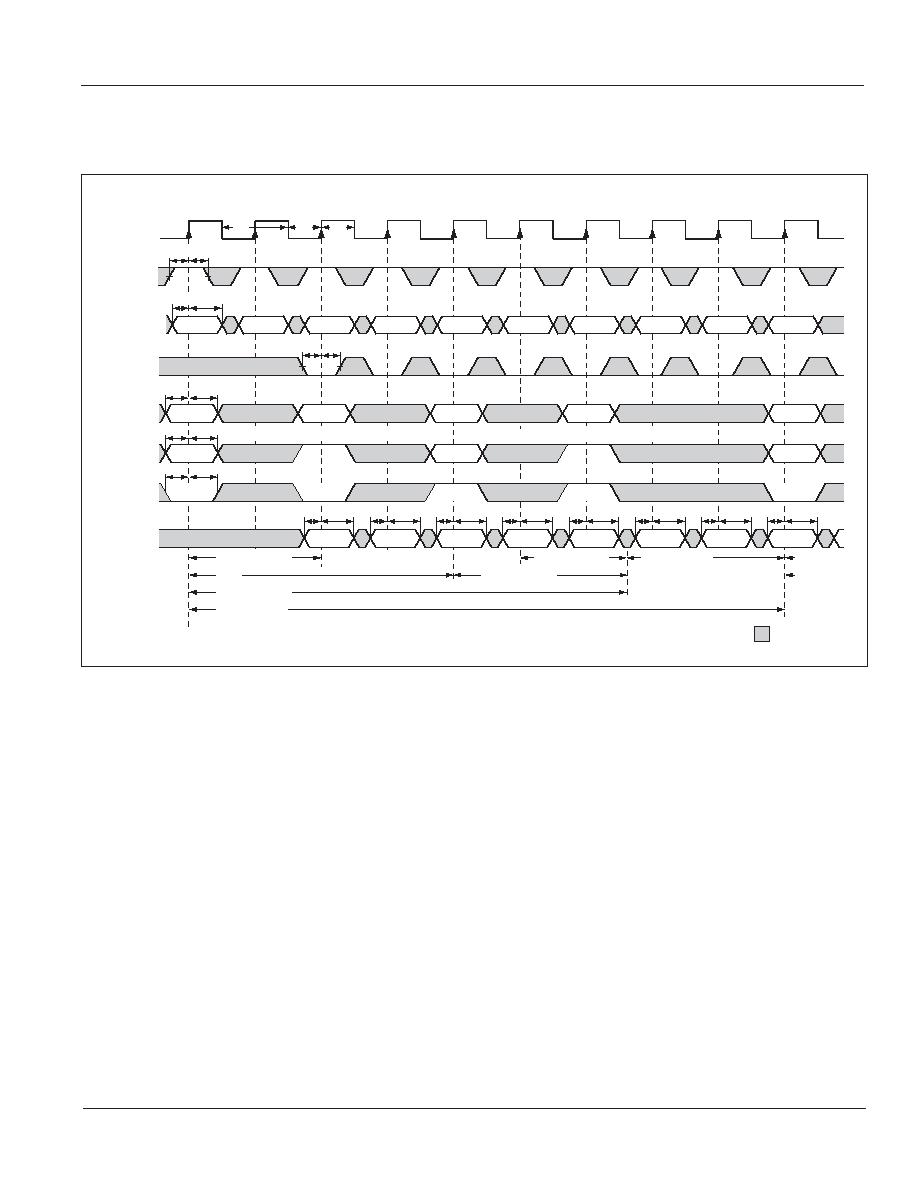
Integrated Silicon Solution, Inc. -- www.issi.com --
1-800-379-4774
43
Rev. E
05/01/06
ISSI
Æ
IS42S81600B, IS42S16800B
ALTERNATING BANK WRITE ACCESSES
BANK 0
BANK 1
BANK 1
BANK 0
DON'T CARE
CLK
CKE
COMMAND
DQM/DQML
DQMH
A0-A9, A11
A10
BA0, BA1
DQ
t
CMS
t
CMH
t
AS
t
AH
t
AS
t
AH
t
AS
t
AH
t
DS
t
DH
t
DS
t
DH
t
DS
t
DH
t
RCD
- BANK 0
t
RCD
- BANK 0
t
DPL
- BANK 1
t
RAS
- BANK 0
t
RC
- BANK 0
t
CH
t
CL
t
CK
t
DS
t
DH
t
DS
t
DH
t
DS
t
DH
t
DS
t
DH
t
DS
t
DH
t
CMS
t
CMH
t
CKS
t
CKH
ACTIVE NOP WRITE NOP ACTIVE NOP WRITE NOP NOP ACTIVE
D
IN
m
D
IN
m+
1
D
IN
m+
2
D
IN
m+
3
D
IN
b
D
IN
b+
1
D
IN
b+
2
D
IN
b+
3
ROW
ROW
BANK 0
ROW ROW
t
RRD
t
RCD
- BANK 1
t
DPL
- BANK 0
t
RP
- BANK 0
COLUMN m
(2)
ROW COLUMN
b
(2)
ROW
ENABLE AUTO PRECHARGE
ENABLE AUTO PRECHARGE
T0 T1 T2 T3 T4 T5 T6 T7 T8 T9
Notes:
1) Burst Length = 4
2) X16: A9 and A11 = "Don't Care"
X8: A11 = "Don't Care"
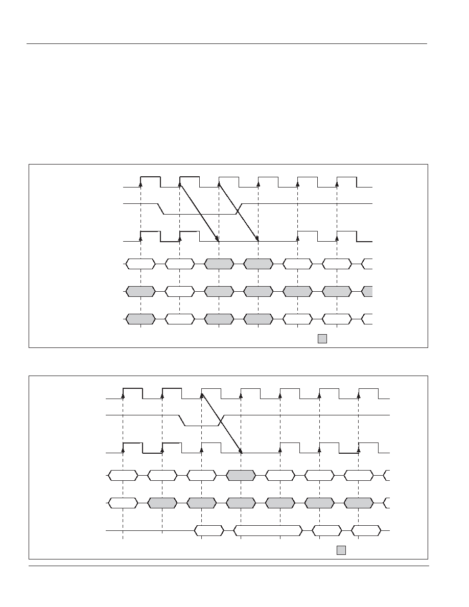
ISSI
Æ
44
Integrated Silicon Solution, Inc. -- www.issi.com --
1-800-379-4774
Rev. E
05/01/06
IS42S81600B, IS42S16800B
DON'T CARE
CLK
CKE
COMMAND
ADDRESS
DQ
T0 T1 T2 T3 T4 T5
NOP
WRITE NOP
NOP
BANK a,
COL n
D
IN
n
D
IN
n+1
D
IN
n+2
INTERNAL
CLOCK
DON'T CARE
CLK
CKE
COMMAND
ADDRESS
DQ
T0 T1 T2 T3 T4 T5 T6
READ NOP NOP
NOP NOP NOP
BANK a,
COL n
D
OUT
n D
OUT
n+1
D
OUT
n+2
D
OUT
n+3
INTERNAL
CLOCK
CLOCK SUSPEND
Clock suspend mode occurs when a column access/burst
is in progress and CKE is registered LOW. In the clock
suspend mode, the internal clock is deactivated, "freezing"
the synchronous logic.
For each positive clock edge on which CKE is sampled
LOW, the next internal positive clock edge is suspended.
Any command or data present on the input pins at the time
of a suspended internal clock edge is ignored; any data
present on the DQ pins remains driven; and burst counters
are not incremented, as long as the clock is suspended.
(See following examples.)
Clock suspend mode is exited by registering CKE HIGH; the
internal clock and related operation will resume on the
subsequent positive clock edge.
Clock Suspend During WRITE Burst
Clock Suspend During READ Burst
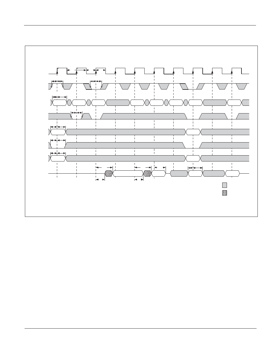
Integrated Silicon Solution, Inc. -- www.issi.com --
1-800-379-4774
45
Rev. E
05/01/06
ISSI
Æ
IS42S81600B, IS42S16800B
CLOCK SUSPEND MODE
Notes:
1)
CAS latency = 3, Burst Length = 2, Auto Precharge is disabled.
2) X16: A9 and A11 = "Don't Care"
X8: A11 = "Don't Care"
DON'T CARE
CLK
CKE
COMMAND
DQM/DQML
DQMH
A0-A9, A11
A10
BA0, BA1
DQ
t
CMS
t
CMH
t
AS
t
AH
t
AS
t
AH
t
AS
t
AH
t
CH
t
CL
t
CK
t
CMS
t
CMH
t
CKS
t
CKH
COLUMN m
(2)
T0 T1 T2 T3 T4 T5 T6 T7 T8 T9
READ NOP NOP
NOP NOP NOP
WRITE
NOP
t
CKS
t
CKH
BANK
BANK
COLUMN n
(2)
t
AC
t
AC
t
OH
t
HZ
D
OUT
m
D
OUT
m+1
t
LZ
UNDEFINED
D
IN
e+1
t
DS
t
DH
D
IN
e
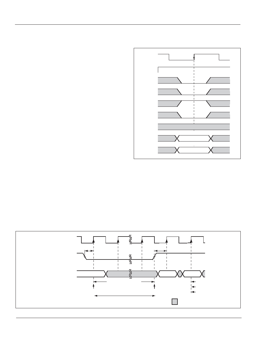
ISSI
Æ
46
Integrated Silicon Solution, Inc. -- www.issi.com --
1-800-379-4774
Rev. E
05/01/06
IS42S81600B, IS42S16800B
CLK
CKE
HIGH
ALL BANKS
BANK SELECT
BANK ADDRESS
CS
RAS
CAS
WE
A0-A9, A11
A10
BA0, BA1
DON'T CARE
CLK
CKE
COMMAND
NOP NOP
ACTIVE
t
CKS
t
CKS
All banks idle
Enter power-down mode
Exit power-down mode
t
RCD
t
RAS
t
RC
Input buffers gated off
less than 64ms
PRECHARGE Command
POWER-DOWN
POWER-DOWN
Power-down occurs if CKE is registered LOW coincident
with a NOP or COMMAND INHIBIT when no accesses are
in progress. If power-down occurs when all banks are idle,
this mode is referred to as precharge power-down; if power-
down occurs when there is a row active in either bank, this
mode is referred to as active power-down. Entering power-
down deactivates the input and output buffers, excluding
CKE, for maximum power savings while in standby. The
device may not remain in the power-down state longer than
the refresh period (64ms) since no refresh operations are
performed in this mode.
The power-down state is exited by registering a NOP or
COMMAND INHIBIT and CKE HIGH at the desired clock
edge (meeting t
CKS
). See figure below.
PRECHARGE
The PRECHARGE command (see figure) is used to deac-
tivate the open row in a particular bank or the open row in all
banks. The bank(s) will be available for a subsequent row
access some specified time (t
RP
) after the PRECHARGE
command is issued. Input A10 determines whether one or
all banks are to be precharged, and in the case where only
one bank is to be precharged, inputs BA0, BA1 select the
bank. When all banks are to be precharged, inputs BA0,
BA1 are treated as "Don't Care." Once a bank has been
precharged, it is in the idle state and must be activated prior
to any READ or WRITE commands being issued to that
bank.
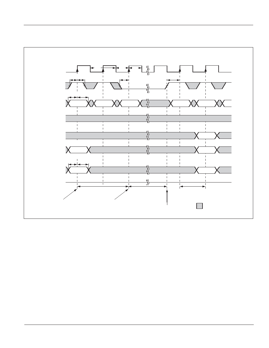
Integrated Silicon Solution, Inc. -- www.issi.com --
1-800-379-4774
47
Rev. E
05/01/06
ISSI
Æ
IS42S81600B, IS42S16800B
POWER-DOWN MODE CYCLE
DON'T CARE
CLK
CKE
COMMAND
DQM/DQML
DQMH
A0-A9, A11
A10
BA0, BA1
DQ
t
AS
t
AH
BANK
t
CH
t
CL
t
CK
t
CMS
t
CMH
t
CKS
t
CKH
PRECHARGE NOP
NOP
NOP
ACTIVE
ALL BANKS
SINGLE BANK
ROW
ROW
BANK
t
CKS
t
CKS
Precharge all
active banks
All banks idle
Two clock cycles
Input buffers gated
off while in
power-down mode
All banks idle, enter
power-down mode
Exit power-down mode
T0 T1 T2
Tn+1
Tn+2
High-Z
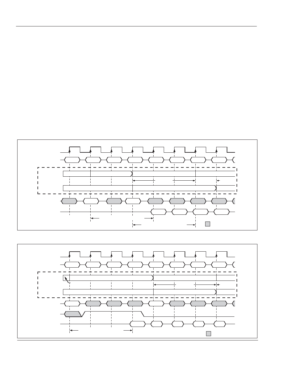
ISSI
Æ
48
Integrated Silicon Solution, Inc. -- www.issi.com --
1-800-379-4774
Rev. E
05/01/06
IS42S81600B, IS42S16800B
DON'T CARE
CLK
COMMAND
BANK n
BANK m
ADDRESS
DQ
T0 T1 T2 T3 T4 T5 T6 T7
NOP
NOP
NOP NOP NOP NOP
D
OUT
a
D
OUT
a+1
D
OUT
b
D
OUT
b+1
BANK n,
COL a
CAS Latency - 3 (BANK n)
CAS Latency - 3 (BANK m)
t
RP - BANK n
t
RP - BANK m
READ - AP
BANK n
READ - AP
BANK m
Page Active
READ with Burst of 4
Interrupt Burst, Precharge
Idle
Page Active
READ with Burst of 4
Precharge
Internal States
BANK n,
COL b
DON'T CARE
CLK
COMMAND
BANK n
BANK m
ADDRESS
DQM
DQ
T0 T1 T2 T3 T4 T5 T6 T7
NOP NOP NOP
NOP NOP NOP
D
OUT
a
D
IN
b
D
IN
b+1
D
IN
b+2
D
IN
b+3
BANK n,
COL a
BANK m,
COL b
CAS Latency - 3 (BANK n)
t
RP - BANK n
t
DPL - BANK m
READ - AP
BANK n
WRITE - AP
BANK m
READ with Burst of 4
Interrupt Burst, Precharge
Idle
Page Active
WRITE with Burst of 4
Write-Back
Internal States
Page Active
BURST READ/SINGLE WRITE
The burst read/single write mode is entered by programming
the write burst mode bit (M9) in the mode register to a logic 1.
In this mode, all WRITE commands result in the access of a
single column location (burst of one), regardless of the
programmed burst length. READ commands access
columns according to the programmed burst length and
sequence, just as in the normal mode of operation (M9 = 0).
CONCURRENT AUTO PRECHARGE
An access command (READ or WRITE) to another bank
while an access command with auto precharge enabled is
executing is not allowed by SDRAMs, unless the SDRAM
supports CONCURRENT AUTO PRECHARGE. ISSI
SDRAMs support CONCURRENT AUTO PRECHARGE.
Four cases where CONCURRENT AUTO PRECHARGE
occurs are defined below.
READ with Auto Precharge
1. Interrupted by a READ (with or without auto precharge):
A READ to bank m will interrupt a READ on bank n, CAS
latency later. The PRECHARGE to bank n will begin
when the READ to bank m is registered.
2. Interrupted by a WRITE (with or without auto precharge):
A WRITE to bank m will interrupt a READ on bank n when
registered. DQM should be used three clocks prior to the
WRITE command to prevent bus contention. The
PRECHARGE to bank n will begin when the WRITE to
bank m is registered.
READ With Auto Precharge interrupted by a READ
READ With Auto Precharge interrupted by a WRITE
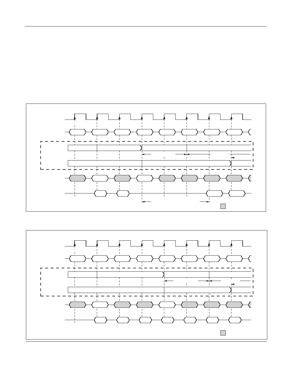
Integrated Silicon Solution, Inc. -- www.issi.com --
1-800-379-4774
49
Rev. E
05/01/06
ISSI
Æ
IS42S81600B, IS42S16800B
DON'T CARE
CLK
COMMAND
BANK n
BANK m
ADDRESS
DQ
T0 T1 T2 T3 T4 T5 T6 T7
NOP
NOP
NOP NOP NOP NOP
D
IN
a
D
IN
a+1
D
OUT
b
D
OUT
b+1
BANK n,
COL a
BANK m,
COL b
CAS Latency - 3 (BANK m)
t
RP - BANK n
t
RP - BANK m
WRITE - AP
BANK n
READ - AP
BANK m
Page Active
WRITE with Burst of 4
Interrupt Burst, Write-Back
Precharge
Page Active
READ with Burst of 4
Precharge
Internal States
t
DPL
- BANK n
DON'T CARE
CLK
COMMAND
BANK n
BANK m
ADDRESS
DQ
T0 T1 T2 T3 T4 T5 T6 T7
NOP
NOP NOP
NOP NOP NOP
BANK n,
COL a
BANK m,
COL b
t
RP - BANK n
t
DPL - BANK m
WRITE - AP
BANK n
WRITE - AP
BANK m
Page Active
WRITE with Burst of 4
Interrupt Burst, Write-Back
Precharge
Page Active
WRITE with Burst of 4
Write-Back
Internal States
t
DPL
- BANK n
D
IN
a
D
IN
a+1
D
IN
a+2
D
IN
b
D
IN
b+1
D
IN
b+2
D
IN
b+3
WRITE with Auto Precharge
3. Interrupted by a READ (with or without auto precharge):
A READ to bank m will interrupt a WRITE on bank n when
registered, with the data-out appearing (CAS latency) later.
The PRECHARGE to bank n will begin after t
DPL
is met,
where t
DPL
begins when the READ to bank m is registered.
The last valid WRITE to bank n will be data-in registered one
clock prior to the READ to bank m.
4. Interrupted by a WRITE (with or without auto precharge):
AWRITE to bank m will interrupt a WRITE on bank n when
registered. The PRECHARGE to bank n will begin after
t
DPL
is met, where t
DPL
begins when the WRITE to bank m
is registered. The last valid data WRITE to bank n will be
data registered one clock prior to a WRITE to bank m.
WRITE With Auto Precharge interrupted by a READ
WRITE With Auto Precharge interrupted by a WRITE
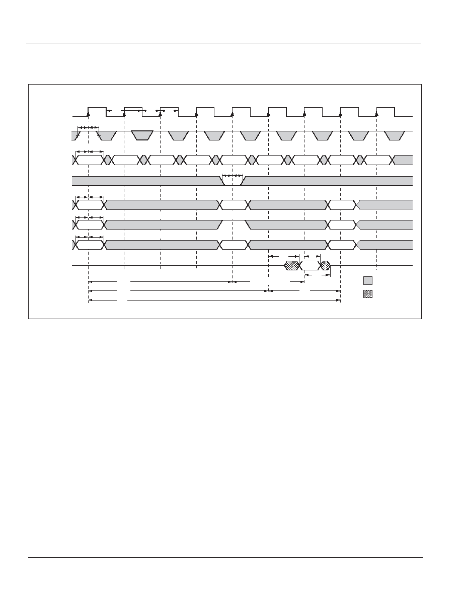
ISSI
Æ
50
Integrated Silicon Solution, Inc. -- www.issi.com --
1-800-379-4774
Rev. E
05/01/06
IS42S81600B, IS42S16800B
SINGLE READ WITH AUTO PRECHARGE
DON'T CARE
UNDEFINED
CLK
CKE
COMMAND
DQM/DQML
DQMH
A0-A9, A11
A10
BA0, BA1
DQ
t
CMS
t
CMH
ACTIVE NOP NOP NOP READ NOP NOP ACTIVE
NOP
t
AS
t
AH
t
AS
t
AH
t
AS
t
AH
ROW
ROW
BANK
COLUMN m
(2)
t
CH
t
CL
t
CK
t
CMS
t
CMH
t
CKS
t
CKH
BANK
t
RCD
t
RAS
t
RC
CAS Latency
t
AC
t
HZ
t
OH
D
OUT
m
T0 T1 T2 T3 T4 T5 T6 T7 T8
t
RP
ENABLE AUTO PRECHARGE
ROW
ROW
BANK
Notes:
1)
CAS latency = 2, Burst Length = 1
2) X16: A9 and A11 = "Don't Care"
X8: A11 = "Don't Care"

Integrated Silicon Solution, Inc. -- www.issi.com --
1-800-379-4774
51
Rev. E
05/01/06
ISSI
Æ
IS42S81600B, IS42S16800B
READ WITH AUTO PRECHARGE
DON'T CARE
UNDEFINED
CLK
CKE
COMMAND
DQM/DQML
DQMH
A0-A9, A11
A10
BA0, BA1
DQ
t
CMS
t
CMH
ACTIVE
NOP READ NOP NOP NOP NOP NOP
ACTIVE
t
AS
t
AH
t
AS
t
AH
t
AS
t
AH
ROW
ROW
BANK
COLUMN m
(2)
t
CH
t
CL
t
CK
t
CMS
t
CMH
t
CKS
t
CKH
BANK
t
RCD
t
RAS
t
RC
CAS Latency
t
AC
t
AC
t
AC
t
AC
t
OH
t
HZ
t
OH
D
OUT
m
t
OH
D
OUT
m+1
t
OH
D
OUT
m+2
D
OUT
m+3
T0 T1 T2 T3 T4 T5 T6 T7 T8
t
RP
ENABLE AUTO PRECHARGE
ROW
ROW
BANK
t
LZ
Notes:
1)
CAS latency = 2, Burst Length = 4
2) X16: A9 and A11 = "Don't Care"
X8: A11 = "Don't Care"

ISSI
Æ
52
Integrated Silicon Solution, Inc. -- www.issi.com --
1-800-379-4774
Rev. E
05/01/06
IS42S81600B, IS42S16800B
SINGLE READ WITHOUT AUTO PRECHARGE
DON'T CARE
UNDEFINED
CLK
CKE
COMMAND
DQM/DQML
DQMH
A0-A9, A11
A10
BA0, BA1
DQ
t
CMS
t
CMH
ACTIVE NOP READ NOP NOP PRECHARGE NOP ACTIVE NOP
t
AS
t
AH
t
AS
t
AH
t
AS
t
AH
ROW
ROW
BANK
COLUMN m
(2)
t
CH
t
CL
t
CK
t
CMS
t
CMH
t
CKS
t
CKH
BANK
t
RCD
t
RAS
t
RC
CAS Latency
t
AC
t
HZ
t
OH
D
OUT
m
T0 T1 T2 T3 T4 T5 T6 T7 T8
t
RP
DISABLE AUTO PRECHARGE
ROW
ROW
BANK
t
LZ
ALL BANKS
SINGLE BANK
BANK
Notes:
1)
CAS latency = 2, Burst Length = 1
2) X16: A9 and A11 = "Don't Care"
X8: A11 = "Don't Care"
Integrated Silicon Solution, Inc. -- www.issi.com --
1-800-379-4774
53
Rev. E
05/01/06
ISSI
Æ
IS42S81600B, IS42S16800B
READ WITHOUT AUTO PRECHARGE
DON'T CARE
UNDEFINED
CLK
CKE
COMMAND
DQM/DQML
DQMH
A0-A9, A11
A10
BA0, BA1
DQ
t
CMS
t
CMH
ACTIVE NOP READ NOP NOP NOP PRECHARGE NOP ACTIVE
t
AS
t
AH
t
AS
t
AH
t
AS
t
AH
ROW
ROW
BANK
COLUMN m
(2)
t
CH
t
CL
t
CK
t
CMS
t
CMH
t
CKS
t
CKH
BANK
t
RCD
CAS Latency
t
AC
t
AC
t
AC
t
AC
t
OH
t
HZ
t
OH
D
OUT
m
t
OH
D
OUT
m+1
t
OH
D
OUT
m+2
D
OUT
m+3
T0 T1 T2 T3 T4 T5 T6 T7 T8
DISABLE AUTO PRECHARGE
ROW
ROW
BANK
t
LZ
t
RAS
t
RC
t
RP
ALL BANKS
SINGLE BANK
BANK
Notes:
1)
CAS latency = 2, Burst Length = 4
2) X16: A9 and A11 = "Don't Care"
X8: A11 = "Don't Care"

ISSI
Æ
54
Integrated Silicon Solution, Inc. -- www.issi.com --
1-800-379-4774
Rev. E
05/01/06
IS42S81600B, IS42S16800B
SINGLE WRITE WITH AUTO PRECHARGE
Notes:
1) Burst Length = 1
2) X16: A9 and A11 = "Don't Care"
X8: A11 = "Don't Care"
DON'T CARE
CLK
CKE
COMMAND
DQM/DQML, DQMH
A0-A9, A11
A10
BA0, BA1
DQ
t
CMS
t
CMH
t
AS
t
AH
t
AS
t
AH
t
AS
t
AH
t
DS
t
DH
t
RCD
t
RAS
t
RC
t
CH
t
CL
t
CK
t
CMS
t
CMH
t
CKS
t
CKH
ACTIVE
NOP NOP NOP
WRITE NOP NOP NOP
ACTIVE
NOP
t
DPL
t
RP
COLUMN m
(2)
ROW
BANK
BANK
ENABLE AUTO PRECHARGE
ROW
ROW
ROW
BANK
D
IN
m
T0 T1 T2 T3 T4 T5 T6 T7 T8 T9
Integrated Silicon Solution, Inc. -- www.issi.com --
1-800-379-4774
55
Rev. E
05/01/06
ISSI
Æ
IS42S81600B, IS42S16800B
SINGLE WRITE - WITHOUT AUTO PRECHARGE
DON'T CARE
CLK
CKE
COMMAND
DQM/DQML
DQMH
A0-A9, A11
A10
BA0, BA1
DQ
t
CMS
t
CMH
t
AS
t
AH
t
AS
t
AH
t
AS
t
AH
t
DS
t
DH
t
RCD
t
RAS
t
RC
t
CH
t
CL
t
CK
t
CMS
t
CMH
t
CKS
t
CKH
ACTIVE NOP WRITE NOP NOP PRECHARGE NOP ACTIVE NOP
t
DPL(3)
t
RP
ROW
ROW
ROW
BANK
D
IN
m
COLUMN m
(2)
ROW
BANK BANK
BANK
ALL BANKS
SINGLE BANK
T0 T1 T2 T3 T4 T5 T6 T7 T8
DISABLE AUTO PRECHARGE
Notes:
1) Burst Length = 1
2) X16: A9 and A11 = "Don't Care"
X8: A11 = "Don't Care"
3) t
RAS
must not be violated.
ISSI
Æ
56
Integrated Silicon Solution, Inc. -- www.issi.com --
1-800-379-4774
Rev. E
05/01/06
IS42S81600B, IS42S16800B
WRITE - WITHOUT AUTO PRECHARGE
DON'T CARE
CLK
CKE
COMMAND
DQM/DQML
DQMH
A0-A9, A11
A10
BA0, BA1
DQ
t
CMS
t
CMH
t
AS
t
AH
t
AS
t
AH
t
AS
t
AH
t
RCD
t
RAS
t
RC
t
CH
t
CL
t
CK
t
CMS
t
CMH
t
CKS
t
CKH
ACTIVE NOP WRITE NOP NOP NOP PRECHARGE NOP ACTIVE
t
DPL(3)
t
RP
COLUMN m
(2)
ROW
DISABLE AUTO PRECHARGE
ROW
ROW
ROW
BANK
t
DS
t
DH
t
DS
t
DH
t
DS
t
DH
t
DS
t
DH
D
IN
m
D
IN
m+
1
D
IN
m+
2
D
IN
m+
3
BANK
BANK BANK
ALL BANKS
SINGLE BANK
T0 T1 T2 T3 T4 T5 T6 T7 T8
Notes:
1) Burst Length = 4
2) X16: A9 and A11 = "Don't Care"
X8: A11 = "Don't Care"
3) t
RAS
must not be violated.
Integrated Silicon Solution, Inc. -- www.issi.com --
1-800-379-4774
57
Rev. E
05/01/06
ISSI
Æ
IS42S81600B, IS42S16800B
WRITE - WITH AUTO PRECHARGE
DON'T CARE
CLK
CKE
COMMAND
DQM/DQML
DQMH
A0-A9, A11
A10
BA0, BA1
DQ
t
CMS
t
CMH
t
AS
t
AH
t
AS
t
AH
t
AS
t
AH
t
RCD
t
RAS
t
RC
t
CH
t
CL
t
CK
t
CMS
t
CMH
t
CKS
t
CKH
ACTIVE NOP
WRITE NOP NOP NOP NOP NOP NOP ACTIVE
t
DPL
t
RP
COLUMN m
(2)
ROW
BANK
BANK
ENABLE AUTO PRECHARGE
ROW
ROW
ROW
BANK
t
DS
t
DH
t
DS
t
DH
t
DS
t
DH
t
DS
t
DH
D
IN
m
D
IN
m+
1
D
IN
m+
2
D
IN
m+
3
T0 T1 T2 T3 T4 T5 T6 T7 T8 T9
Notes:
1) Burst Length = 4
2) X16: A9 and A11 = "Don't Care"
X8: A11 = "Don't Care"

ISSI
Æ
58
Integrated Silicon Solution, Inc. -- www.issi.com --
1-800-379-4774
Rev. E
05/01/06
IS42S81600B, IS42S16800B
ORDERING INFORMATION - V
DD
= 3.3V
Commercial Range: 0
∞∞
∞∞
∞C to 70∞∞∞∞∞C
Frequency
Speed (ns)
Order Part No.
Package
167 MHz
6
IS42S81600B-6T
54-Pin TSOPII
143 MHz
7
IS42S81600B-7T
54-Pin TSOPII
Frequency
Speed (ns)
Order Part No.
Package
167 MHz
6
IS42S16800B-6T
54-Pin TSOPII
143 MHz
7
IS42S16800B-7T
54-Pin TSOPII
ORDERING INFORMATION - V
DD
= 3.3V
Industrial Range: -40
∞∞
∞∞
∞C to 85∞∞∞∞∞C
Frequency
Speed (ns)
Order Part No.
Package
143 MHz
7
IS42S81600B-7TI
54-Pin TSOPII
Frequency
Speed (ns)
Order Part No.
Package
143 MHz
7
IS42S16800B-7TI
54-Pin TSOPII

Integrated Silicon Solution, Inc. -- www.issi.com --
1-800-379-4774
59
Rev. E
05/01/06
ISSI
Æ
IS42S81600B, IS42S16800B
ORDERING INFORMATION - V
DD
= 3.3V
Commercial Range: 0
∞∞
∞∞
∞C to 70∞∞∞∞∞C
Frequency
Speed (ns)
Order Part No.
Package
167 MHz
6
IS42S81600B-6TL
54-Pin TSOPII, Lead-free
143 MHz
7
IS42S81600B-7TL
54-Pin TSOPII, Lead-free
Frequency
Speed (ns)
Order Part No.
Package
167 MHz
6
IS42S16800B-6TL
54-Pin TSOPII, Lead-free
143 MHz
7
IS42S16800B-7TL
54-Pin TSOPII, Lead-free
133 MHz
7.5
IS42S16800B-75ETL
54-Pin TSOPII, Lead-free
ORDERING INFORMATION - V
DD
= 3.3V
Industrial Range: -40
∞∞
∞∞
∞C to 85∞∞∞∞∞C
Frequency
Speed (ns)
Order Part No.
Package
143 MHz
7
IS42S81600B-7TLI
54-Pin TSOPII, Lead-free
Frequency
Speed (ns)
Order Part No.
Package
167 MHz
6
IS42S16800B-6TLI
54-Pin TSOPII, Lead-free
143 MHz
7
IS42S16800B-7TLI
54-Pin TSOPII, Lead-free
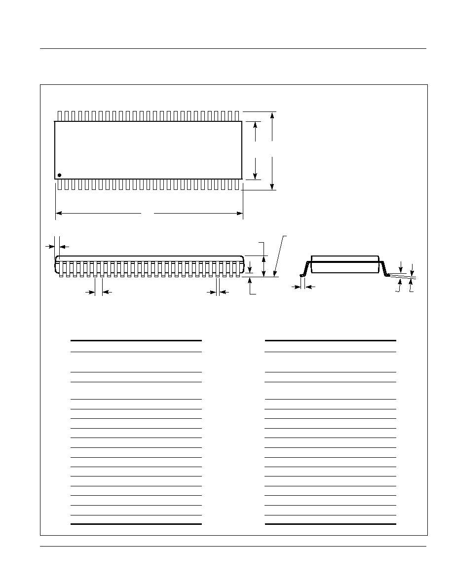
PACKAGING INFORMATION
ISSI
Æ
Integrated Silicon Solution, Inc. -- 1-800-379-4774
1
Rev. C
01/28/02
Plastic TSOP 54≠Pin, 86-Pin
Package Code: T (Type II)
Plastic TSOP (T - Type II)
Millimeters
Inches
Symbol
Min
Max
Min
Max
Ref. Std.
No. Leads (N)
54
A
--
1.20
--
0.047
A1
0.05
0.15
0.002
0.006
A2
--
--
--
--
b
0.30
0.45
0.012
0.018
C
0.12
0.21
0.005
0.0083
D
22.02 22.42
0.867
0.8827
E1
10.03 10.29
0.395
0.405
E
11.56 11.96
0.455
0.471
e
0.80 BSC
0.031 BSC
L
0.40
0.60
0.016
0.024
L1
--
--
--
--
ZD 0.71 REF
0∞
8∞
0∞
8∞
D
SEATING PLANE
b
e
C
1
N/2
N/2+1
N
E1
A1
A
E
L
ZD
Notes:
1. Controlling dimension: millimieters,
unless otherwise specified.
2. BSC = Basic lead spacing between
centers.
3. Dimensions D and E1 do not include
mold flash protrusions and
should be
measured from the bottom of the
package
.
4. Formed leads shall be planar with
respect to one another within 0.004
inches at the seating plane.
Plastic TSOP (T - Type II)
Millimeters
Inches
Symbol
Min
Max
Min
Max
Ref. Std.
No. Leads (N)
86
A
--
1.20
--
0.047
A1
0.05
0.15
0.002
0.006
A2
0.95
1.05
0.037
0.041
b
0.17
0.27
0.007
0.011
C
0.12
0.21
0.005
0.008
D
22.02 22.42
0.867
0.8827
E1
10.16 BSC
0.400 BSC
E
11.56 11.96
0.455
0.471
e
0.50 BSC
0.020 BSC
L
0.40
0.60
0.016
0.024
L1
0.80 REF
0.031 REF
ZD 0.61 REF 0.024 BSC
0∞
8∞
0∞
8∞