©1996 IXYS Corporation. All rights reserved.
IXYS Semiconductor GmbH
Edisonstr.15, D-68623 Lampertheim, Germany
Phone: +49-6206-5030 Fax: +49-6206-503627
IXYS Corporation
3540 Bassett Street; Santa Clara, CA 95054
Tel: 408-982-0700; Fax: 408-496-0670
IXSH10N120AU1
∑
Symbol
Test Conditions
Maximum Ratings
V
CES
T
J
= 25∞C to 150∞C
1200
V
V
CGR
T
J
= 25∞C to 150∞C; R
GE
= 1 M
1200
V
V
GES
Continuous
±20
V
V
GEM
Transient
±30
V
I
C25
T
C
= 25∞C
20
A
I
C90
T
C
= 90∞C
10
A
I
CM
T
C
= 25∞C, 1 ms
40
A
SSOA
V
GE
= 15 V, T
J
= 125∞C, R
G
= 150
I
CM
= 20
A
(RBSOA)
Clamped inductive load, L = 300 µH
@ 0.8 V
CES
t
sc
T
J
= 125∫C, V
CE
= 720 V; V
GE
= 15V, R
G
= 150
5
µs
P
C
T
C
= 25∞C
100
W
T
J
-55 ... +150
∞C
T
JM
150
∞C
T
STG
-55 ... +150
∞C
M
d
Mounting torque
1.15/10
Nm/lb-in.
.
Weight
6
g
Max. Lead Temperature for
300
∞C
Soldering (1.6mm from case for 10s)
94523C (1/96)
Features
∑
High voltage IGBT with
guaranteed short circuit SOA capability.
∑
IGBT with anti-parallel diode in one
package
∑
2
nd
generation HDMOS
TM
process
Low VCE(sat)
- for minimum on-state conduction
losses
∑
MOS Gate turn-on
- drive simplicity
Applications
∑
AC motor speed control
∑
DC servo and robot drives
∑
Uninterruptible power supplies (UPS)
∑
Switched-mode and resonant-mode
power supplies
∑
DC choppers
Advantages
∑
Saves space (two devices in one
package
∑
Easy to mount(isolated mounting
hole)
∑
Reduces assembly time and cost
∑
Runs cooler than equivalent
6-pack IGBTs
∑
Easier to package to meet UL
requirements
IGBT with Diode
"S" Series - Improved SCSOA Capability
PRELIMINARY DATA SHEET
Symbol
Test Conditions
Characteristic Values
(T
J
= 25∞C unless otherwise specified)
Min. Typ.
Max.
BV
CES
I
C
= 3.25 mA, V
GE
= 0 V
1200
V
V
GE(th)
I
C
= 750
µ
A, V
CE
= V
GE
4
8
V
I
CES
V
CE
= 0.8 V
CES
,V
GE
= 0 V
T
J
= 25∞C
400
µA
Note 2
T
J
= 125∞C
5
mA
I
GES
V
CE
= 0 V, V
GE
= ±20 V
+ 100
nA
V
CE(sat)
I
C
= I
C90
, V
GE
= 15 V
4.0
V
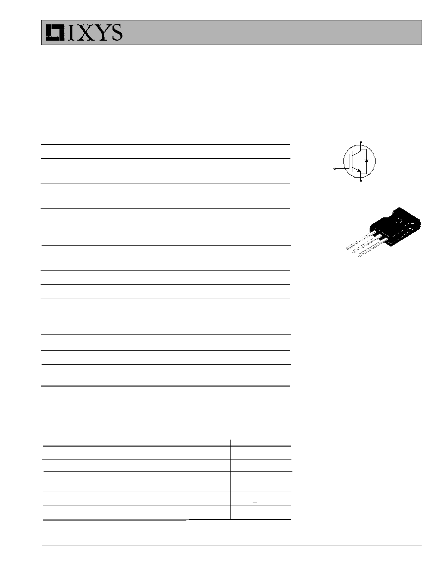
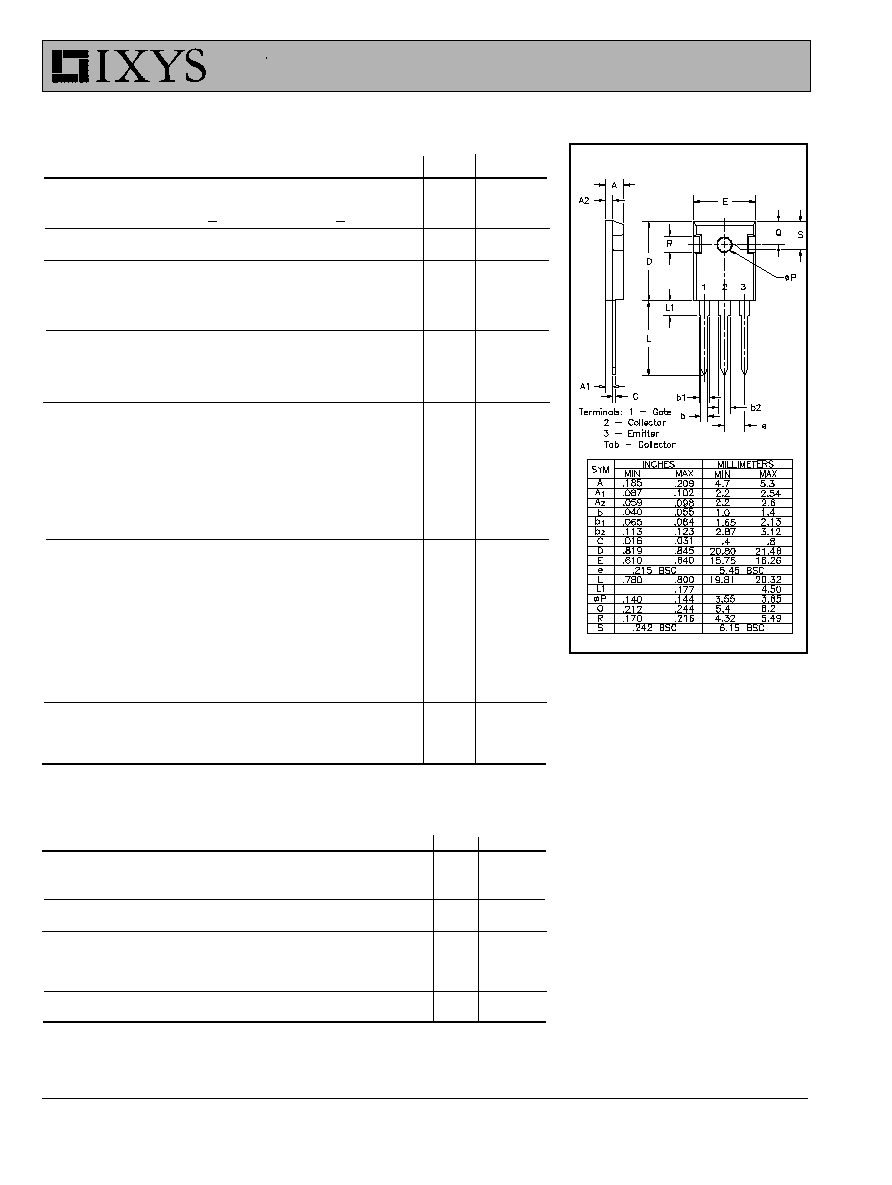
TO-247AD
G
C
E
I
C25
= 20 A
V
CES
= 1200 V
V
CE(sat)
= 4.0 V
E
G
C
IXYS Corporation
3540 Bassett Street; Santa Clara, CA 95054
Tel: 408-982-0700; Fax: 408-496-0670
IXYS Semiconductor GmbH
Edisonstr. 15, D-68623 Lampertheim, Germany
Phone: +49-6206-5030 Fax: +49-6206-503627
IXYS reserves the right to change limits, test conditions, and dimensions.
IXSH10N120AU1
g
fs
I
C
= I
C90
,
V
CE
= 10 V,
4
S
Pulse test, t < 300 µs, duty cycle
< 2 %
I
C(on)
V
GE
= 15V, V
CE
= 10 V
37
A
C
ies
V
CE
= 25 V, V
GE
= 0 V, f = 1 MHz
800
pF
C
oes
53
pF
C
res
15
pF
Q
g
I
C
= I
c90
, V
GE
= 15 V, V
CE
= 0.5 V
CES
40
nC
Q
ge
12
nC
Q
gc
20
nC
t
d(on)
Inductive load, T
J
= 25∞C
100
ns
t
ri
I
C
= I
C90
, V
GE
= 15 V, L = 300µH
200
ns
t
d(off)
R
G
= 120
, V
CLAMP
= 0.8 V
CES
250
ns
t
fi
Note 1
620
ns
t
c
750
ns
E
off
2.5
mJ
t
d(on)
Inductive load, T
J
= 125∞C
100
ns
t
ri
I
C
= I
C90,
V
GE
= 15 V, L = 300µH
200
ns
E
(on)
R
G
= 120
TBD
mJ
t
d(off)
V
CLAMP
= 0.8 V
CES
300
ns
t
fi
Note 1
1100
ns
t
c
1200
ns
E
off
4.0
mJ
R
thJC
1.25 K/W
R
thCK
0.25
K/W
Symbol
Test Conditions
Characteristic Values
(T
J
= 25∞C unless otherwise specified)
Min. Typ.
Max.
TO-247AD (IXSH)
Reverse Diode (FRED)
Characteristic Values
(TJ = 25∫C unless otherwise specified)
Min.
Typ.
Max.
V
F
I
F
= I
C90
, V
GE
= 0V
2.6
V
Pulse test, t< 300 µs, duty cycle < 2% T
J
= 125∫C
2.3
t
rr
I
F
= 1A; di/dt = -50A/µs; V
R
= 30V; T
J
= 25∫C
50
70
ns
I
RM
I
F
= I
C90
, V
GE
= 0V, -di
F
/dt = 100 A/µs
6.5
7.2
A
t
rr
T
J
= 100∫C, V
R
= 540V
300
ns
R
thJC
2.0 K/W
Notes:
1. Switching times may increase for V
CE
(Clamp) > 0.8 V
CES
, higher T
J
or Rg values.
2. Device must be heatsunk for high temperature leakage current measurements to
avoid thermal runaway.