Preliminary
IXYS
MX841
1
03/10/05
Drawing No. 17023
www.ixys.net
MX841
White LED Step-Up Converter
Features:
� 1.1V to 5.5V Input Range
� 2 Amp Peak Switch Current
� High Efficiency > 80%
� 20V Maximum Output with Over-Voltage
Protection
� LED Intensity Control
� 1.0 MHz Fixed Frequency Switching
� 8 Lead SOIC Package
Applications:
� White LED Display Backlighting
-
Low Voltage: Mobile Phones, PDA's,
MP3 Players, Digital Cameras
-
High Drive Current: Vehicle
Instrumentation Panels
Ordering Information
Part No.
Description
Qty
17000-00TU SOIC-8
Standard Tube
100
17000-00TR SOIC-8
Standard T&R
2500
17043-00TU SOIC-8
Exposed Pad Tube
100
17043-00TR SOIC-8
Exposed Pad T&R
2500
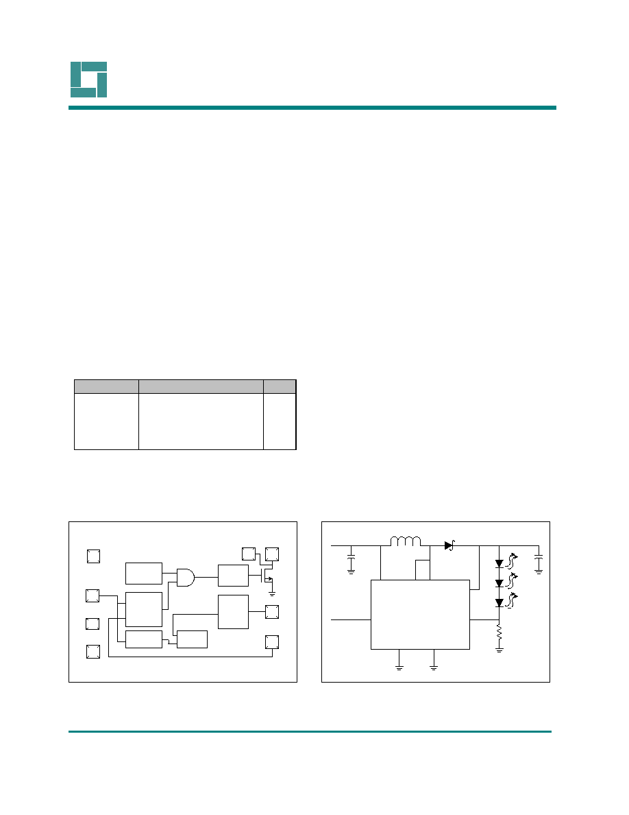
General Description
The MX841 is a fixed frequency, constant current
source step-up DC/DC converter. The output current
is directly regulated making the MX841 ideal for
driving series connected white light emitting diodes
(LED's) in backlight applications. The MX841
powers up to 3 series white LED's at 1.1V, and 20
series/parallel white LED's at 5.0V.
The MX841 features a 1.0MHz switching frequency
to accommodate the use of small capacitors and a
small inductor necessary in size sensitive portable
applications. Light intensity and shutdown are
conveniently controlled by a single analog voltage.
Power efficiency and battery life are extended
through the use of a high voltage, low R
DSON
N-
channel MOSFET switch.
The MX841 is designed to operate over a
temperature range of -40�C to +85�C, and is
available in an SOIC-8 Package, with or without an
Exposed Pad in Tube or on Tape and Reel.
(Alternate package types available upon request).
Functional Block Diagram
Typical Application
MX841
CTRL
Vbattery
VDD
SW
OVD
Isense
CTL/
SLEEP
Rsense
Vboost
Analog
GND
Switch
GND
SW
3
1
4
5
6
8
7
2
osc
err amp/
comparato
r
sleep de
t
bias gen
VDD
drive
r
Isense
OVD
band gap
+
compar
e
Gnd
Switch
SW
SW
CTL/SLEEP
Analog
Gnd

MX841
IXYS
Absolute Maximum Ratings
(Voltages with respect to GND=0V)
Parameter
Min
Max
Unit
V
DD
Supply Voltage
-0.4
+6.5
V
CTRL Voltage
G
ND
-0.4
V
DD
+0.4 V
I
SENSE
Voltage
G
ND
-0.4
V
DD
+0.4 V
SW Voltage
-0.4
+24.0
V
OVD Voltage
-0.4
+24.0
V
Operating Ambient Temperature Range
-40
+85
C
o
Storage Temperature Range
-55
+150
C
o
Operating Junction Temperature Range
-40
+125
C
o
Standard SOIC
JA
= 114�C/W
775 mW
Power Dissipation
T
A
= 27�C
Exposed Pad SOIC
JA
= 50�C/W
1.75 W
ESD Warning
ESD (electrostatic discharge) sensitive device. Although the MX841 features proprietary ESD protection circuitry,
permanent damage may be sustained if subjected to high energy electrostatic discharges. Proper ESD precautions
are recommended to avoid performance degradation or loss of functionality.
DC Electrical Characteristics
V
DD
=3.0V, R
SENSE
=5, V
CTRL
=1.0V, L=6.8�H, C
BYP
=1�F, T
A
= -40
o
C to +85
o
C, Typical Values at +25
o
C
Unless otherwise specified
Parameter
Condition
Min
Typ
Max
Unit
Supply Voltage
T
A
= 25
o
C
1.1
5.5
V
Supply Current Overvoltage
Not Switching: V
CTRL
= 260mV
V
RSENSE
> 13 X V
CTRL
0.5
0.8
Supply Current Operating
Switching: V
CTRL
= V
DD,
V
RSENSE
=GND 2
mA
T
A
= +25
o
C
6
�A
Sleep Current
V
CTRL
< 100mV
T
A
= +85
o
C
7
�A
CTRL Bias Current
-10
�A
I
SENSE
Bias Current
-7
�A
V
CTRL
>260mV
20
�A
OVD Bias Current
OVD
= 18V
V
CTRL
= GND
0
OVD
Rising
22
V
Over Voltage Threshold
OVD Falling
18.5
V
CTRL / V
RSENSE
13
V/V
V
CTRL
Rising
260
mV
V
CTRL
Sleep Mode
V
CTRL
Falling
100
mV
V
SW
= 0.1V
1.9
SW On Resistance
V
SW
= 0.5V
2.2
V
DD
=1.2V, L=33�H
30
mA
Switch Current
V
DD
=5.5V, L=2.5�H
2
A
SW Voltage Range
V
DD
-
V
SCHOTTKY
20 V
T
A
= +25
o
C
0.1
�A
SW Leakage Current
OVD
= V
SW
= 18V
T
A
= +85
o
C
0.3
�A
V
CTRL
0
V
DD
V
Absolute Maximum Ratings are
stress ratings. Stresses in excess of
these ratings can cause permanent
damage to the device. Functional
operation of the device at these or
any other conditions beyond those
indicated in the operational sections
of this data sheet is not implied.
Exposure of the device to the
absolute maximum ratings for an
extended period may degrade the
device and affect its reliability.
Preliminary
MX841
2
03/10/05
Drawing No. 17023
www.ixys.net
MX841
IXYS
AC Electrical Characteristics
V
DD
=3.0V, R
SENSE
=5; V
CTRL
=1.0V, L=6.8�H; C
BYP
=1�F, T
A
= -40
o
C to +85
o
C, Typical Values at +25
o
C
Unless otherwise specified
Parameter
Condition
Min
Typ
Max
Unit
Oscillator Frequency
0.6
1.0
1.3
MHz
Duty Cycle
72.5
%
Pin Description
Pin No.
Pin Name
Description
1, 4
SW
Power Switch. Connects the drain of the internal high voltage N-channel
MOSFET to the Inductor and Schottky Diode to generate the LED boost
voltage. This voltage is determined by the total forward bias voltage of the
LED series string and the Isense resistor value. (Note: Both pins must be
connected.)
2
Analog GND
Analog Ground (Note: Must be connected to a low noise ground source.)
3
Switch GND
Switch Ground (Note: Must be connected to a high current ground source.)
5 VDD
Input supply pin. Input range from 1.1 to 5.5 volts. Must be bypassed with a
low ESR capacitor to GND.
6 OVD
Over Voltage Detect input. Compares the LED boots voltage to the internal
voltage reference. If the boost voltage rises above 22V the OVD circuit
disables the oscillator and N-channel MOSFET until the boost voltage falls
below 18.5V. Must be bypassed with a low ESR capacitor to GND.
7 CTRL
Shutdown and Intensity Control Input. A control voltage above 260mV
enables device operation. A control voltage below 100mV disables device
operation. LED intensity is linearly adjusted with voltages between 260mV
and V
DD
.
8 Isense
Current Sense Input. The LED bias current is set by connecting a carbon
composite or monolithic resistor from this input to Ground. I
SENSE
regulates
this current to 1/13
of the CTRL input voltage.
Preliminary
MX841
3
03/10/05
Drawing No. 17023
www.ixys.net

Preliminary
MX841
4
03/10/05
MX841
IXYS
Functional Description
The MX841 is specifically designed to be
operated from a single cell battery source. The
step-up voltage necessary for the constant
current source to drive up to 5 white LED's in
series, or multiple strings of white LED's, is
achieved with minimal external components. (See
Application Schematics on pages 1&4).
Setting the LED Current
The regulated output current is determined by the
selection of the sense Resistor connected from
the I
SENSE
input to ground, and the maximum user
defined voltage of the CTRL input. The desired
output current, (typically 15mA to 20mA for white
LEDs), is derived using the following formula for
the R
SENSE
value: R
SENSE
= (V
CTRL
X 1/13) / I
LED
.
Current Regulation / Light Intensity Control
The I
SENSE
voltage is fed into an
ErrorAmp/Comparator. The user defined Control
Voltage applied at the CTRL input is scaled by a
gain factor of 1/13 and compared to the I
SENSE
voltage. If the scaled control voltage is greater
than the I
SENSE
voltage, the 1.0MHz oscillator
signal driving the N-Channel MOSFET will be
enabled. Once the I
SENSE
voltage reaches the
scaled CTRL voltage the oscillator signal is
modulated on and off by the
ErrorAmp/Comparator to maintain the desired
regulated output current.
Light intensity is controlled by reducing the
voltage at the CTRL input. As the CTRL input
voltage is reduced below the user defined
maximum value, the oscillator signal driving the
N-Channel MOSFET is interrupted by the
ErrorAmp/Comparator. The pulse skip modulating
of the N-Channel MOSFET causes a reduction in
the regulated current equal to the ratio of the
reduced CTRL voltage to the maximum CTRL
voltage.
Sleep Mode
The MX841 goes into sleep mode when the V
CTRL
input is less than 100mV. All circuits except V
CTRL
detection are shutdown and the supply current
falls to 6uA. Once the V
CTRL
input rises above
260mV the MX841 resumes normal operation.
Over Voltage Detection
The MX841 will go into a shutdown state to avoid
an over voltage condition if the current path
between the SW output and the R
SENSE
input is
interrupted. A voltage reference and comparator
circuit evaluates the voltage potential at the OVD
input and shuts down the oscillator and N-
Channel MOSFET if an over voltage condition is
detected. Normal operation is resumed once the
OVD input voltage falls below the reference
voltage, (20V typical).
Drawing No. 17023
www.ixys.net
MX841
IXYS
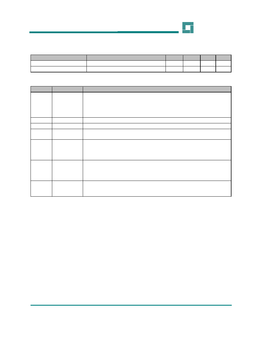
Circuit Application Driving 15 White LED's
MX841
CTRL
Vbattery 3.0V - 5.0V
VD
D
SW
OVD
Isense
CTL/SLEEP
Rsense
Vboost
1N5817
V
F
=0.3V
6.8uH
I
pk
=1.7A
20K Ohms
22uF 35V
0.1uF in Parallel
5 Ohms
5 Ohms
5 Ohms
22uF 35V
0.1uF in Parallel
26K Ohms @ 3.0V
57K Ohms @ 5.0V
(Dimming Control)
SW
Analog
GND
Switch
GND
2
1
4
6
8
5
7
3
IXYS Corporation makes no representations or warranties with respect to the accuracy or completeness of the contents of this
publication and reserves the right to make changes to specifications and product descriptions at any time without notice. Neither
circuit patent licenses nor indemnity are expressed or implied. Except as set forth in IXYS' Standard Terms and Conditions of Sale,
IXYS Corporation assumes no liability whatsoever, and disclaims any expressed or implied warranty, relating to its products
including, but not limited to, the implied warranty of merchantability, fitness for a particular purpose, or infringement of any
intellectual property right
.
Preliminary
MX841
5
03/10/05
Drawing No. 17023
www.ixys.net
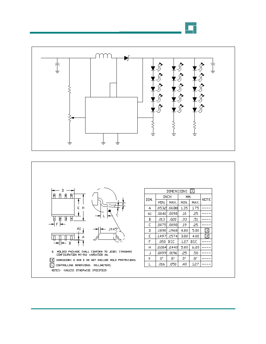
8-LEAD SOI