1 - 2
© 2000 IXYS All rights reserved
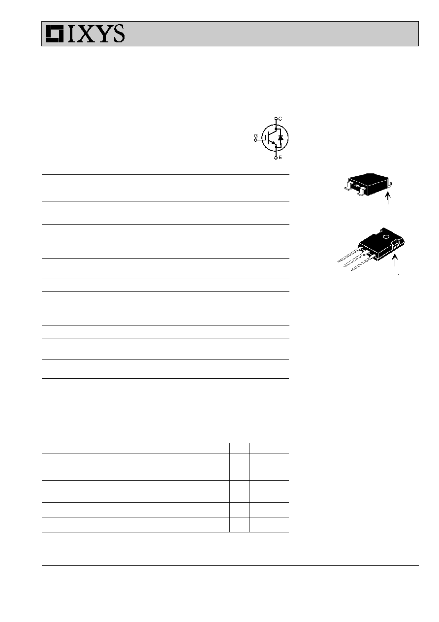
G = Gate,
C = Collector,
E = Emitter,
TAB = Collector
Symbol
Test Conditions
Maximum Ratings
V
CES
T
J
= 25
∞
C to 150
∞
C
600
V
V
CGR
T
J
= 25
∞
C to 150
∞
C; R
GE
= 1 M
W
600
V
V
GES
Continuous
±
20
V
V
GEM
Transient
±
30
V
I
C25
T
C
= 25
∞
C
40
A
I
C90
T
C
= 90
∞
C
20
A
I
CM
T
C
= 25
∞
C, 1 ms
80
A
SSOA
V
GE
= 15 V, T
VJ
= 125
∞
C, R
G
= 22
W
I
CM
= 40
A
(RBSOA)
Clamped inductive load, L = 100
m
H
@ 0.8 V
CES
P
C
T
C
= 25
∞
C
150
W
T
J
-55 ... +150
∞
C
T
JM
150
∞
C
T
stg
-55 ... +150
∞
C
M
d
Mounting torque (M3) TO-247AD
1.13/10 Nm/lb.in.
Maximum lead temperature for soldering
300
∞
C
1.6 mm (0.062 in.) from case for 10 s
Weight
TO-247AD
6
g
TO-268
4
g
Symbol
Test Conditions
Characteristic Values
(T
J
= 25
∞
C, unless otherwise specified)
min.
typ.
max.
BV
CES
I
C
= 250
m
A, V
GE
= 0 V
600
V
V
GE(th)
I
C
= 250
m
A, V
CE
= V
GE
2.5
5.5
V
I
CES
V
CE
= 0.8 ∑ V
CES
T
J
= 25
∞
C
200
m
A
V
GE
= 0 V
T
J
= 150
∞
C
3
mA
I
GES
V
CE
= 0 V, V
GE
=
±
20 V
±
100
nA
V
CE(sat)
I
C
= I
C90
, V
GE
= 15 V
1.7
2.0
V
HiPerFAST
TM
IGBT
V
CES
= 600 V
with Diode
I
C25
= 40 A
V
CE(sat)typ
= 1.7 V
t
fi(typ)
= 100 ns
98566A (3/99)
IXGH 20N60BD1
IXGT 20N60BD1
C (TAB)
G
C
E
TO-247 AD
(IXGH)
TO-268
(IXGT)
G
E
C (TAB)
Features
∑ International standard packages
∑ High frequency IGBT and antiparallel
FRED in one package
∑ High current handling capability
∑ HiPerFAST
TM
HDMOS
TM
process
∑ MOS Gate turn-on
-drive simplicity
Applications
∑ Uninterruptible power supplies (UPS)
∑ Switched-mode and resonant-mode
power supplies
∑ AC motor speed control
∑ DC servo and robot drives
∑ DC choppers
Advantages
∑ Space savings (two devices in one
package)
∑ High power density
∑ Suitable for surface mounting
∑ Very low switching losses for high
frequency applications
∑ Easy to mount with 1 screw,TO-247
(insulated mounting screw hole)
Preliminary data
IXYS reserves the right to change limits, test conditions, and dimensions.
2 - 2
© 2000 IXYS All rights reserved
Symbol
Test Conditions
Characteristic Values
(T
J
= 25
∞
C, unless otherwise specified)
min.
typ.
max.
g
fs
I
C
= I
C90
; V
CE
= 10 V,
9
17
S
Pulse test, t
£
300
m
s, duty cycle
£
2 %
C
ies
1500
pF
C
oes
V
CE
= 25 V, V
GE
= 0 V, f = 1 MHz
150
pF
C
res
40
pF
Q
g
55
nC
Q
ge
I
C
= I
C90
, V
GE
= 15 V, V
CE
= 0.5 V
CES
12
nC
Q
gc
20
nC
t
d(on)
15
ns
t
ri
25
ns
t
d(off)
110
200
ns
t
fi
100
150
ns
E
off
0.7
1.0
mJ
t
d(on)
15
ns
t
ri
35
ns
E
on
0.75
mJ
t
d(off)
220
ns
t
fi
140
ns
E
off
1.2
mJ
R
thJC
0.83 K/W
R
thCK
TO-247
0.25
K/W
Reverse Diode (FRED)
Characteristic Values
(T
J
= 25
∞
C, unless otherwise specified)
Symbol
Test Conditions
min.
typ.
max.
V
F
I
F
= 30A, V
GE
= 0 V,
T
J
= 150
∞
C
1.6
V
Pulse test, t
£
300
m
s, duty cycle d
£
2 % T
J
= 25
∞
C
2.5
V
I
RM
I
F
= 30A, V
GE
= 0 V, -di
F
/dt = 100 A/
m
s
6
A
t
rr
V
R
= 100 V
T
J
=100
∞
C
100
ns
I
F
= 1 A; -di/dt = 100 A/
m
s; V
R
= 30 V T
J
= 25
∞
C
25
ns
R
thJC
1.0 K/W
Inductive load, T
J
= 25
∞
C
I
C
= I
C90
, V
GE
= 15 V, L = 100
m
H,
V
CE
= 0.8 V
CES
, R
G
= R
off
= 10
W
Remarks: Switching times may increase
for V
CE
(Clamp) > 0.8 ∑ V
CES
, higher T
J
or
increased R
G
Inductive load, T
J
= 125
∞
C
I
C
= I
C90
, V
GE
= 15 V, L = 100
m
H
V
CE
= 0.8 V
CES
, R
G
= R
off
= 10
W
Remarks: Switching times may increase
for V
CE
(Clamp) > 0.8 ∑ V
CES
, higher T
J
or
increased R
G
IXGH 20N60BD1
IXGT 20N60BD1
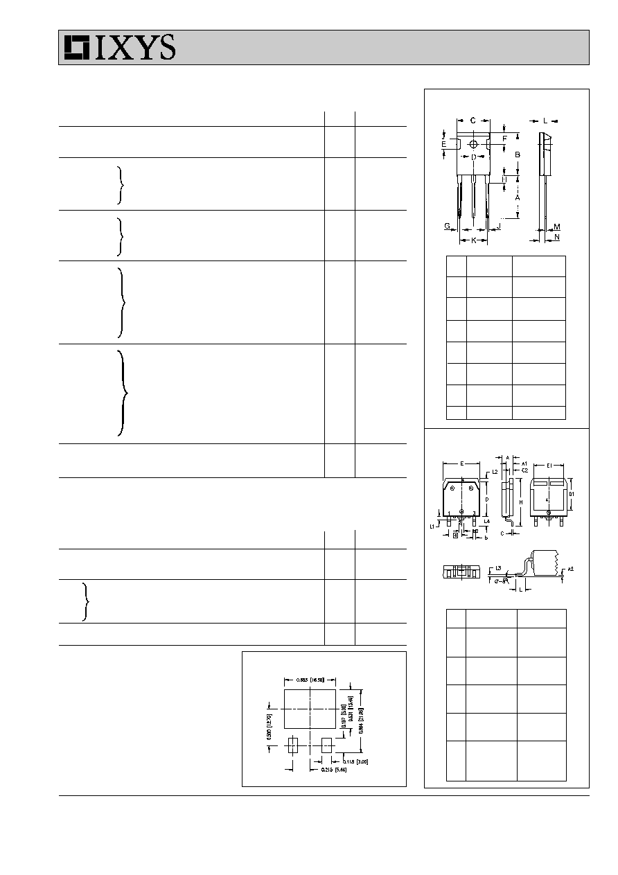
TO-247 AD (IXGH) Outline
Dim. Millimeter
Inches
Min.
Max.
Min.
Max.
A
19.81 20.32
0.780 0.800
B
20.80 21.46
0.819 0.845
C
15.75 16.26
0.610 0.640
D
3.55
3.65
0.140 0.144
E
4.32
5.49
0.170 0.216
F
5.4
6.2
0.212 0.244
G
1.65
2.13
0.065 0.084
H
-
4.5
-
0.177
J
1.0
1.4
0.040 0.055
K
10.8
11.0
0.426 0.433
L
4.7
5.3
0.185 0.209
M
0.4
0.8
0.016 0.031
N
1.5
2.49
0.087 0.102
TO-268AA (D
3
PAK)
Dim.
Millimeter
Inches
Min.
Max.
Min.
Max.
A
4.9
5.1
.193
.201
A
1
2.7
2.9
.106
.114
A
2
.02
.25
.001
.010
b
1.15
1.45
.045
.057
b
2
1.9
2.1
.75
.83
C
.4
.65
.016
.026
D
13.80
14.00
.543
.551
E
15.85
16.05
.624
.632
E
1
13.3
13.6
.524
.535
e 5.45 BSC .215 BSC
H
18.70
19.10
.736
.752
L
2.40
2.70
.094
.106
L1
1.20
1.40
.047
.055
L2
1.00
1.15
.039
.045
L3 0.25 BSC .010 BSC
L4
3.80
4.10
.150
.161
Min. Recommended Footprint
IXYS MOSFETS and IGBTs are covered by one or more of the following U.S. patents:
4,835,592
4,881,106
5,017,508
5,049,961
5,187,117
5,486,715
4,850,072
4,931,844
5,034,796
5,063,307
5,237,481
5,381,025