© 1997 IXYS All rights reserved
Preliminary data
HiP
HiP
HiP
HiP
HiPerF
erF
erF
erF
erFAST
AST
AST
AST
AST
TM
TM
TM
TM
TM
IGBT
IGBT
IGBT
IGBT
IGBT
with Diode
with Diode
with Diode
with Diode
with Diode
Combi P
Combi P
Combi P
Combi P
Combi Pac
ac
ac
ac
ack
k
k
k
k
Symbol
Symbol
Symbol
Symbol
Symbol
Test Conditions
Test Conditions
Test Conditions
Test Conditions
Test Conditions
Characteristic Values
Characteristic Values
Characteristic Values
Characteristic Values
Characteristic Values
(T
J
= 25
∞
C, unless otherwise specified)
min.
min.
min.
min.
min.
typ.
typ.
typ.
typ.
typ.
max.
max.
max.
max.
max.
BV
BV
BV
BV
BV
CES
CES
CES
CES
CES
I
C
= 250
µ
A, V
GE
= 0 V
500
V
V
V
V
V
V
GE(th)
GE(th)
GE(th)
GE(th)
GE(th)
I
C
= 250
µ
A, V
CE
= V
GE
2.5
5.5
V
II
II
I
CES
CES
CES
CES
CES
V
CE
= 0.8 ∑ V
CES
T
J
= 25
∞
C
200
µ
A
V
GE
= 0 V
T
J
= 125
∞
C
8
mA
II
II
I
GES
GES
GES
GES
GES
V
CE
= 0 V, V
GE
=
±
20 V
±
100
nA
V
V
V
V
V
CE(sat)
CE(sat)
CE(sat)
CE(sat)
CE(sat)
I
C
= I
C90
, V
GE
= 15 V
2.1
2.5
V
Features
Features
Features
Features
Features
∑
International standard packages
JEDEC TO-247 SMD surface
mountable and JEDEC TO-247 AD
∑
High frequency IGBT and antiparallel
FRED in one package
∑
High current handling capability
∑
HiPerFAST
TM
HDMOS
TM
process
∑
MOS Gate turn-on
- drive simplicity
Applications
Applications
Applications
Applications
Applications
∑
Uninterruptible power supplies (UPS)
∑
Switched-mode and resonant-mode
power supplies
∑
AC motor speed control
∑
DC servo and robot drives
∑
DC choppers
Advantages
Advantages
Advantages
Advantages
Advantages
∑
Space savings (two devices in one
package)
∑
High power density
∑
Suitable for surface mounting
∑
Very low switching losses for high
frequency applications
∑
Easy to mount with 1 screw,TO-247
(insulated mounting screw hole)
Symbol
Symbol
Symbol
Symbol
Symbol
Test Conditions
Test Conditions
Test Conditions
Test Conditions
Test Conditions
Maximum Ratings
Maximum Ratings
Maximum Ratings
Maximum Ratings
Maximum Ratings
V
V
V
V
V
CES
CES
CES
CES
CES
T
J
= 25
∞
C to 150
∞
C
500
V
V
V
V
V
V
CGR
CGR
CGR
CGR
CGR
T
J
= 25
∞
C to 150
∞
C; R
GE
= 1 M
500
V
V
V
V
V
V
GES
GES
GES
GES
GES
Continuous
±
20
V
V
V
V
V
V
GEM
GEM
GEM
GEM
GEM
Transient
±
30
V
II
II
I
C25
C25
C25
C25
C25
T
C
= 25
∞
C
44
A
II
II
I
C90
C90
C90
C90
C90
T
C
= 90
∞
C
22
A
II
II
I
CM
CM
CM
CM
CM
T
C
= 25
∞
C, 1 ms
88
A
SSOA
SSOA
SSOA
SSOA
SSOA
V
GE
= 15 V, T
VJ
= 125
∞
C, R
G
= 22
I
CM
= 44
A
(RBSOA)
(RBSOA)
(RBSOA)
(RBSOA)
(RBSOA)
Clamped inductive load, L = 100
µ
H
@ 0.8 V
CES
P
P
P
P
P
C
C
C
C
C
T
C
= 25
∞
C
150
W
T
T
T
T
T
J
J
J
J
J
-55 ... +150
∞
C
T
T
T
T
T
JM
JM
JM
JM
JM
150
∞
C
T
T
T
T
T
stg
stg
stg
stg
stg
-55 ... +150
∞
C
Maximum Lead and Tab temperature for soldering
300
∞
C
1.6 mm (0.062 in.) from case for 10 s
M
M
M
M
M
d
d
d
d
d
Mounting torque, TO-247 AD
1.13/10 Nm/lb.in.
Weight
Weight
Weight
Weight
Weight
TO-247 SMD
4
g
TO-247 AD
6
g
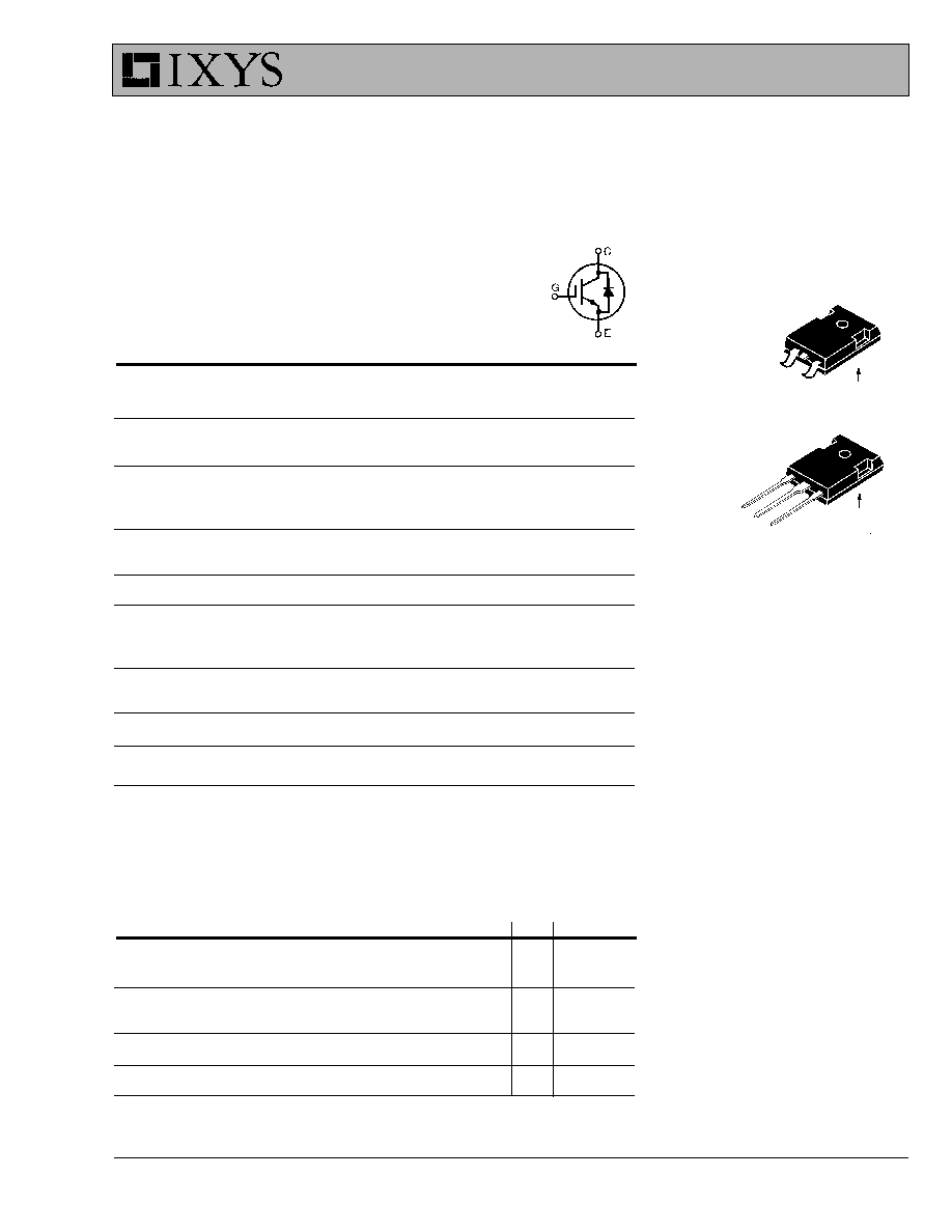
C (TAB)
G
C
E
G
E
C (TAB)
V
CES
= 500 V
I
C(25)
=
44 A
V
CE(sat)typ
=
2.1 V
t
fi(typ)
= 55 ns
G = Gate,
C = Collector,
E = Emitter,
TAB = Collector
*Add suffix letter "S" for surface mountable
package
TO-247 SMD*
TO-247 SMD*
TO-247 SMD*
TO-247 SMD*
TO-247 SMD*
TO-247 AD
TO-247 AD
TO-247 AD
TO-247 AD
TO-247 AD
97509(2/97)
IXGH22N50B
IXGH22N50B
IXGH22N50B
IXGH22N50B
IXGH22N50BU1
U1
U1
U1
U1
IXGH22N50B
IXGH22N50B
IXGH22N50B
IXGH22N50B
IXGH22N50BU1S
U1S
U1S
U1S
U1S
IXYS MOSFETS and IGBTs are covered by one or more of the following U.S. patents:
4,835,592
4,881,106
5,017,508
5,049,961
5,187,117
5,486,715
4,850,072
4,931,844
5,034,796
5,063,307
5,237,481
5,381,025
IXYS reserves the right to change limits, test conditions, and dimensions.
IXGH22N50B
IXGH22N50B
IXGH22N50B
IXGH22N50B
IXGH22N50BU1
U1
U1
U1
U1
IXGH22N50B
IXGH22N50B
IXGH22N50B
IXGH22N50B
IXGH22N50BU1S
U1S
U1S
U1S
U1S
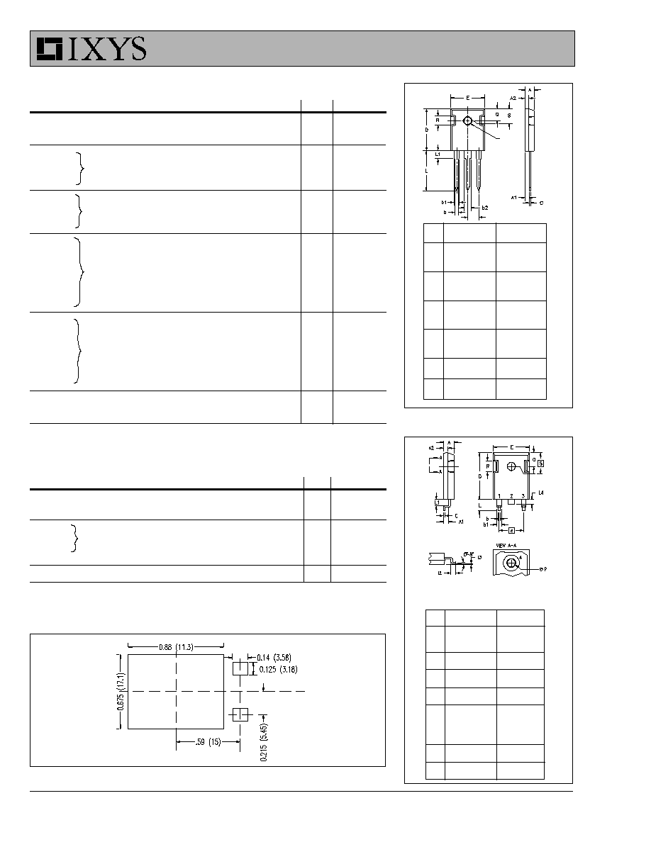
Dim.
Millimeter
Inches
Min.
Max.
Min.
Max.
A
4.7
5.3
.185
.209
A
1
2.2
2.54
.087
.102
A
2
2.2
2.6
.059
.098
b
1.0
1.4
.040
.055
b
1
1.65
2.13
.065
.084
b
2
2.87
3.12
.113
.123
C
.4
.8
.016
.031
D
20.80
21.46
.819
.845
E
15.75
16.26
.610
.640
e
5.20
5.72
0.205 0.225
L
19.81
20.32
.780
.800
L1
4.50
.177
P
3.55
3.65
.140
.144
Q
5.89
6.40
0.232 0.252
R
4.32
5.49
.170
.216
S
6.15 BSC
242 BSC
e
P
1. Gate
2. Collector
3. Emitter
4. Collector
Dim.
Millimeter
Inches
Min.
Max.
Min.
Max.
A
4.83
5.21
.190
.205
A1
2.29
2.54
.090
.100
A2
1.91
2.16
.075
.085
b
1.14
1.40
.045
.055
b1
1.91
2.13
.075
.084
C
0.61
0.80
.024
.031
D
20.80
21.34
.819
.840
E
15.75
16.13
.620
.635
e
5.45
BSC
.215
BSC
L
4.90
5.10
.193
.201
L1
2.70
2.90
.106
.114
L2
2.10
2.30
.083
.091
L3
0.00
0.10
.00
.004
L4
1.90
2.10
.075
.083
ÿP
3.55
3.65
.140
.144
Q
5.59
6.20
.220
.244
R
4.32
4.83
.170
.190
S
6.15
BSC
.242
BSC
TO-247 SMD Outline
TO-247 AD Outline
Inductive load, T
Inductive load, T
Inductive load, T
Inductive load, T
Inductive load, T
J
J
J
J
J
= 125
= 125
= 125
= 125
= 125
∞∞
∞∞
∞
C
C
C
C
C
I
C
= I
C90
, V
GE
= 15 V, L = 100
µ
H
V
CE
= 0.8 V
CES
, R
G
= R
off
= 10
Note 1
Symbol
Symbol
Symbol
Symbol
Symbol
Test Conditions
Test Conditions
Test Conditions
Test Conditions
Test Conditions
Characteristic Values
Characteristic Values
Characteristic Values
Characteristic Values
Characteristic Values
(T
J
= 25
∞
C, unless otherwise specified)
min.
min.
min.
min.
min.
typ.
typ.
typ.
typ.
typ.
max.
max.
max.
max.
max.
g
g
g
g
g
fs
fs
fs
fs
fs
I
C
= I
C90
; V
CE
= 10 V,
9
16
S
Pulse test, t
300
µ
s, duty cycle
2 %
C
C
C
C
C
ies
ies
ies
ies
ies
1450
pF
C
C
C
C
C
oes
oes
oes
oes
oes
V
CE
= 25 V, V
GE
= 0 V, f = 1 MHz
120
pF
C
C
C
C
C
res
res
res
res
res
37
pF
Q
Q
Q
Q
Q
g
g
g
g
g
90
nC
Q
Q
Q
Q
Q
ge
ge
ge
ge
ge
I
C
= I
C90
, V
GE
= 15 V, V
CE
= 0.5 V
CES
11
nC
Q
Q
Q
Q
Q
gc
gc
gc
gc
gc
30
nC
tt
tt
t
d(on)
d(on)
d(on)
d(on)
d(on)
15
ns
tt
tt
t
ri
ri
ri
ri
ri
30
ns
E
E
E
E
E
on
on
on
on
on
0.15
mJ
tt
tt
t
d(off)
d(off)
d(off)
d(off)
d(off)
100
150
ns
tt
tt
t
fi
fi
fi
fi
fi
55
110
ns
E
E
E
E
E
off
off
off
off
off
Note 1
0.3
0.5
mJ
tt
tt
t
d(on)
d(on)
d(on)
d(on)
d(on)
15
ns
tt
tt
t
ri
ri
ri
ri
ri
30
ns
E
E
E
E
E
on
on
on
on
on
0.15
mJ
tt
tt
t
d(off)
d(off)
d(off)
d(off)
d(off)
140
ns
tt
tt
t
fi
fi
fi
fi
fi
100
ns
E
E
E
E
E
off
off
off
off
off
0.6
mJ
R
R
R
R
R
thJC
thJC
thJC
thJC
thJC
0.83 K/W
R
R
R
R
R
thCK
thCK
thCK
thCK
thCK
0.25
K/W
Reverse Diode (FRED)
Reverse Diode (FRED)
Reverse Diode (FRED)
Reverse Diode (FRED)
Reverse Diode (FRED)
Characteristic Values
Characteristic Values
Characteristic Values
Characteristic Values
Characteristic Values
(T
J
= 25
∞
C, unless otherwise specified)
Symbol
Symbol
Symbol
Symbol
Symbol
Test Conditions
Test Conditions
Test Conditions
Test Conditions
Test Conditions
min.
min.
min.
min.
min.
typ.
typ.
typ.
typ.
typ.
max.
max.
max.
max.
max.
V
V
V
V
V
F
F
F
F
F
I
F
= I
C90
, V
GE
= 0 V,
1.6
V
Pulse test, t
300
µ
s, duty cycle d
2 %
II
II
I
RM
RM
RM
RM
RM
I
F
= I
C90
, V
GE
= 0 V, -di
F
/dt = 240 A/
µ
s
10
15
A
tt
tt
t
rr
rr
rr
rr
rr
V
R
= 360 V
T
J
=125
∞
C
150
ns
I
F
= 1 A; -di/dt = 100 A/
µ
s; V
R
= 30 V T
J
=
25
∞
C
35
50
ns
R
R
R
R
R
thJC
thJC
thJC
thJC
thJC
1 K/W
Inductive load, T
Inductive load, T
Inductive load, T
Inductive load, T
Inductive load, T
J
J
J
J
J
= 25
= 25
= 25
= 25
= 25
∞∞
∞∞
∞
C
C
C
C
C
I
C
= I
C90
, V
GE
= 15 V, L = 100
µ
H,
V
CE
= 0.8 V
CES
, R
G
= R
off
= 10
Min. Recommended Footprint (Dimensions in inches and mm)
Note 1: Switching times may increase for V
CE
(Clamp) > 0.8 ∑ V
CES
, higher T
J
or increased R
G