 | –≠–ª–µ–∫—Ç—Ä–æ–Ω–Ω—ã–π –∫–æ–º–ø–æ–Ω–µ–Ω—Ç: 30N60AU1 | –°–∫–∞—á–∞—Ç—å:  PDF PDF  ZIP ZIP |

1 - 6
© 2000 IXYS All rights reserved
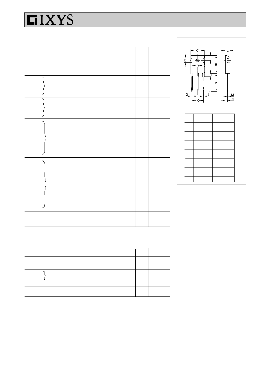
TO-247 AD
V
CES
I
C25
V
CE(sat)
Low V
CE(sat)
IGBT with Diode
IXSH
30
N60U1
600 V
50 A
2.5 V
High Speed IGBT with Diode
IXSH
30
N60AU1
600 V
50 A
3.0 V
Combi Packs
Short Circuit SOA Capability
G
C
E
G = Gate,
C = Collector,
E = Emitter,
TAB = Collector
Symbol
Test Conditions
Maximum Ratings
V
CES
T
J
= 25
∞
C to 150
∞
C
600
V
V
CGR
T
J
= 25
∞
C to 150
∞
C; R
GE
= 1 M
W
600
V
V
GES
Continuous
±
20
V
V
GEM
Transient
±
30
V
I
C25
T
C
= 25
∞
C
50
A
I
C90
T
C
= 90
∞
C
30
A
I
CM
T
C
= 25
∞
C, 1 ms
100
A
SSOA
V
GE
= 15 V, T
J
= 125
∞
C, R
G
= 33
W
I
CM
= 60
A
(RBSOA)
Clamped inductive load, L = 100
m
H
@ 0.8 V
CES
t
SC
V
GE
= 15 V, V
CE
= 360 V, T
J
= 125
∞
C
10
m
s
(SCSOA)
R
G
= 33
W,
non repetitive
P
C
T
C
= 25
∞
C
200
W
T
J
-55 ... +150
∞
C
T
JM
150
∞
C
T
stg
-55 ... +150
∞
C
M
d
Mounting torque
1.13/10
Nm/lb.in.
Weight
6
g
Maximum lead temperature for soldering
300
∞
C
1.6 mm (0.062 in.) from case for 10 s
Symbol
Test Conditions
Characteristic Values
(T
J
= 25
∞
C, unless otherwise specified)
min.
typ.
max.
BV
CES
I
C
= 750
m
A, V
GE
= 0 V
600
V
V
GE(th)
I
C
= 2.5 mA, V
CE
= V
GE
5
8
V
I
CES
V
CE
= 0.8 ∑ V
CES
T
J
= 25
∞
C
500
m
A
V
GE
= 0 V
T
J
= 125
∞
C
8
mA
I
GES
V
CE
= 0 V, V
GE
=
±
20 V
±
100
nA
V
CE(sat)
I
C
= I
C90
, V
GE
= 15 V
30N60U1
2.5
V
30N60AU1
3.0
V
Features
∑ International standard package
JEDEC TO-247 AD
∑ High frequency IGBT with guaranteed
Short Circuit SOA capability
∑ IGBT and anti-parallel FRED in one
package
∑ 2nd generation HDMOS
TM
process
∑ Low V
CE(sat)
- for low on-state conduction losses
∑ MOS Gate turn-on
- drive simplicity
Applications
∑ AC motor speed control
∑ DC servo and robot drives
∑ DC choppers
∑ Uninterruptible power supplies (UPS)
∑ Switch-mode and resonant-mode
power supplies
Advantages
∑ Space savings (two devices in one
package)
∑ Easy to mount with 1 screw
(isolated mounting screw hole)
∑ Reduces assembly time and cost
∑ High power density
92714F (12/96)
IXYS reserves the right to change limits, test conditions, and dimensions.
2 - 6
© 2000 IXYS All rights reserved
Symbol
Test Conditions
Characteristic Values
(T
J
= 25
∞
C, unless otherwise specified)
min.
typ.
max.
g
fs
I
C
= I
C90
; V
CE
= 10 V,
7
13
S
Pulse test, t
£
300
m
s, duty cycle
£
2 %
I
C(on)
V
GE
= 15 V, V
CE
= 10 V
100
A
C
ies
2760
pF
C
oes
V
CE
= 25 V, V
GE
= 0 V, f = 1 MHz
240
pF
C
res
51
pF
Q
g
110
150
nC
Q
ge
I
C
= I
C90
, V
GE
= 15 V, V
CE
= 0.5 V
CES
34
45
nC
Q
gc
47
63
nC
t
d(on)
60
ns
t
ri
130
ns
t
d(off)
400
ns
t
fi
30N60U1
400
ns
30N60AU1
200
ns
E
off
30N60AU1
2.5
mJ
t
d(on)
60
ns
t
ri
130
ns
E
on
4.2
mJ
t
d(off)
30N60U1
540
1000
ns
30N60AU1
340
525
ns
t
fi
30N60U1
600
1500
ns
30N60AU1
340
700
ns
E
off
30N60U1
12
mJ
30N60AU1
6
mJ
R
thJC
0.63 K/W
R
thCK
0.25
K/W
Reverse Diode (FRED)
Characteristic Values
(T
J
= 25
∞
C, unless otherwise specified)
Symbol
Test Conditions
min.
typ.
max.
V
F
I
F
= I
C90
, V
GE
= 0 V,
1.6
V
Pulse test, t
£
300
m
s, duty cycle d
£
2 %
I
RM
I
F
= I
C90
, V
GE
= 0 V, -di
F
/dt = 240 A/
m
s
10
15
A
t
rr
V
R
= 360 V
T
J
= 125
∞
C
150
ns
I
F
= 1 A; -di/dt = 100 A/
m
s; V
R
= 30 V
T
J
= 25
∞
C
35
50
ns
R
thJC
1 K/W
Inductive load, T
J
= 125
∞
C
I
C
= I
C90
, V
GE
= 15 V,
L = 100
m
H
V
CE
= 0.8 V
CES
, R
G
= 4.7
W
Remarks: Switching times
may increase for
V
CE
(Clamp) > 0.8 ∑ V
CES
, higher
T
J
or increased R
G
Inductive load, T
J
= 25
∞
C
I
C
= I
C90
, V
GE
= 15 V, L = 100
m
H,
V
CE
= 0.8 V
CES
, R
G
= 4.7
W
Remarks: Switching times
may increase for
V
CE
(Clamp) > 0.8 ∑ V
CES
,
higher T
J
or increased R
G
IXSH 30N60U1
IXSH 30N60AU1
TO-247 AD (IXSH) Outline
Dim. Millimeter
Inches
Min.
Max.
Min.
Max.
A
19.81 20.32
0.780 0.800
B
20.80 21.46
0.819 0.845
C
15.75 16.26
0.610 0.640
D
3.55
3.65
0.140 0.144
E
4.32
5.49
0.170 0.216
F
5.4
6.2
0.212 0.244
G
1.65
2.13
0.065 0.084
H
-
4.5
-
0.177
J
1.0
1.4
0.040 0.055
K
10.8
11.0
0.426 0.433
L
4.7
5.3
0.185 0.209
M
0.4
0.8
0.016 0.031
N
1.5
2.49
0.087 0.102
IXYS MOSFETS and IGBTs are covered by one or more of the following U.S. patents:
4,835,592
4,881,106
5,017,508
5,049,961
5,187,117
5,486,715
4,850,072
4,931,844
5,034,796
5,063,307
5,237,481
5,381,025

3 - 6
© 2000 IXYS All rights reserved
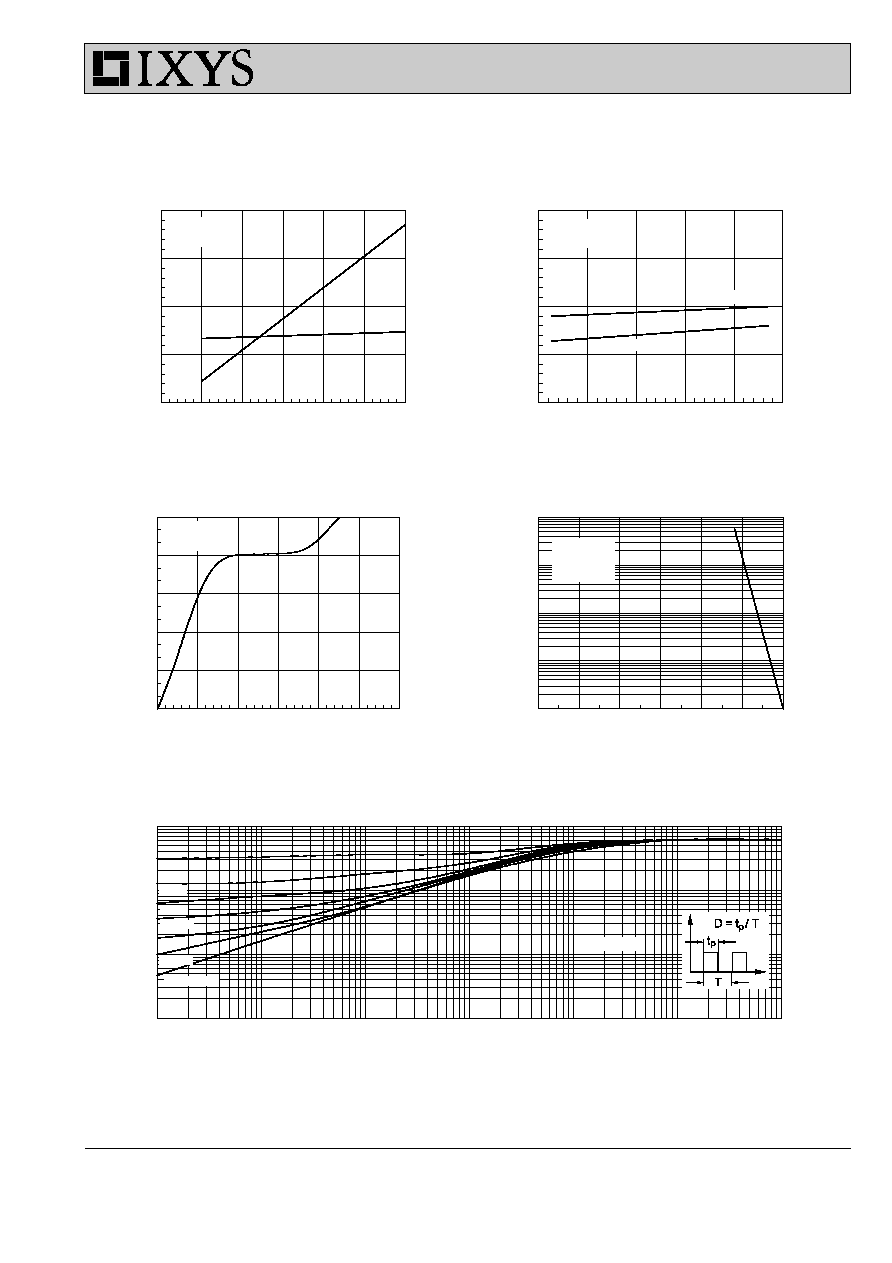
T
J
- Degrees C
-50
-25
0
25
50
75
100 125 150
BV /
V
GE
(
t
h)
- N
o
rm
a
liz
e
d
0.7
0.8
0.9
1.0
1.1
1.2
1.3
V
GE
- Volts
5
6
7
8
9
10 11 12 13
14 15
I
C
-
Am
per
es
0
10
20
30
40
50
60
T
J
- Degrees C
-50
-25
0
25
50
75
100 125 150
V
CE
(
s
a
t
)
- No
r
m
a
liz
e
d
0.6
0.8
1.0
1.2
1.4
1.6
1.8
V
GE
- Volts
8
9
10
11
12
13
14
15
V
CE
- V
o
lts
0
1
2
3
4
5
6
7
8
9
10
V
CE
- Volts
0
2
4
6
8
10
12 14 16 18 20
I
C
-
Am
per
es
0
20
40
60
80
100
9V
11V
13V
V
CE
- Volts
0
1
2
3
4
5
I
C
-
Am
per
es
0
10
20
30
40
50
60
11V
9V
13V
T
J
= 25∞C
V
GE
= 15V
T
J
= 25∞C
I
C
= 15A
I
C
= 30A
I
C
= 60A
T
J
= 25∞C
I
C
= 15A
I
C
= 30A
I
C
= 60A
V
GE
= 15V
T
J
= - 40∞C
T
J
= 125∞C
T
J
= 25∞C
V
CE
= 10V
V
GE(th)
I
C
= 2.5mA
BV
CES
I
C
= 3mA
V
GE
= 15V
7V
Fig.3 Collector-Emitter Voltage
Fig.4 Temperature Dependence
vs. Gate-Emitter Voltage
of Output Saturation Voltage
Fig.5 Input Admittance
Fig.6 Temperature Dependence of
Breakdown and Threshold Voltage
Fig.1 Saturation Characteristics
Fig.2 Output Characterstics
IXSH 30N60U1
IXSH 30N60AU1
4 - 6
© 2000 IXYS All rights reserved
Pulse Width - Seconds
0.00001
0.0001
0.001
0.01
0.1
1
10
Zt
h
JC
(K
/W
)
0.001
0.01
0.1
1
Single pulse
D=0.5
V
CE
- Volts
0
100
200
300
400
500
600
I
C
-
Am
per
e
s
0.01
0.1
1
10
100
Q
g
- nanocoulombs
0
25
50
75
100
125
150
V
GE
- V
o
l
t
s
0
3
6
9
12
15
R
G
- Ohms
0
10
20
30
40
50
E
off
-
m
i
ll
ij
o
u
l
e
s
0.0
2.5
5.0
7.5
10.0
t
fi
-
nanos
econd
s
0
250
500
750
1000
I
C
- Amperes
0
10
20
30
40
50
60
E
of
f
-
mi
l
l
i
J
oul
es
0.0
2.5
5.0
7.5
10.0
t
fi
-
nanos
econ
ds
0
250
500
750
1000
E
off
(-A)
hi-speed
t
fi
(-A)
hi-speed
D = Duty Cycle
T
J
= 125∞C
R
G
= 10
W
t
fi
(-A), hi-speed
E
off
(-A), hi-speed
T
J
= 125∞C
I
C
= 30A
I
C
= 30A
V
CE
= 300V
T
J
= 125∞C
R
G
= 4.7
W
dV/dt < 6V/ns
D=0.01
D=0.02
D=0.05
D=0.1
D=0.2
Fig.11 Transient Thermal Impedance
Fig.9 Gate Charge Characteristic Curve
Fig.10 Turn-Off Safe Operating Area
Fig.7 Turn-Off Energy per Pulse and
Fig.8 Dependence of Turn-Off Energy
Fall Time on Collector Current
Per Pulse and Fall Time on R
G
IXSH 30N60U1
IXSH 30N60AU1

5 - 6
© 2000 IXYS All rights reserved
di
F
/dt - A/µs
0
200
400
600
t
rr
-
nan
os
e
c
on
ds
0.0
0.2
0.4
0.6
0.8
di
F
/dt - A/µs
200
400
600
I
RM
-
Am
per
es
0
10
20
30
40
di
F
/dt - A/µs
1
10
100
1000
Q
r
-
nano
c
o
u
l
om
bs
0
1
2
3
4
T
J
- Degrees C
0
40
80
120
160
Nor
m
al
i
z
ed I
RM
/Q
r
0.0
0.2
0.4
0.6
0.8
1.0
1.2
1.4
Q
r
I
RM
di
F
/dt - A/µs
0
100
200
300
400
500
600
t
fr
-
nanoseconds
0
200
400
600
800
1000
V
FR
- V
o
lts
0
5
10
15
20
25
t
fr
V
FR
Voltage Drop - Volts
0.5
1.0
1.5
2.0
2.5
C
u
r
r
ent
-
Am
per
es
0
20
40
60
80
100
T
J
= 150∞C
T
J
= 100∞C
T
J
= 25∞C
T
J
= 125∞C
I
F
= 37A
typ.
I
F
= 60A
I
F
= 30A
I
F
= 15A
I
F
= 30A
T
J
= 100∞C
V
R
= 350V
T
J
= 100∞C
V
R
= 350V
T
J
= 100∞C
V
R
= 350V
typ.
I
F
= 60A
I
F
= 30A
I
F
= 15A
max.
I
F
= 30A
max.
I
F
= 30A
typ.
I
F
= 60A
I
F
= 30A
I
F
= 15A
max.
Fig.14 Junction Temperature Dependence
Fig.15 Reverse Recovery Chargee
off I
RM
and Q
r
Fig.16 Peak Reverse Recovery Current
Fig.17 Reverse Recovery Time
Fig.12 Maximum Forward Voltage Drop
Fig.13 Peak Forward Voltage V
FR
and
Forward Recovery Time t
fr
IXSH 30N60U1
IXSH 30N60AU1

6 - 6
© 2000 IXYS All rights reserved
Pulse Width - Seconds
0.001
0.01
0.1
1
R
th
JC
- K
/
W
0.01
0.10
1.00
Fig.18 Diode Transient Thermal resistance junction to case
IXSH 30N60U1
IXSH 30N60AU1