 | –≠–ª–µ–∫—Ç—Ä–æ–Ω–Ω—ã–π –∫–æ–º–ø–æ–Ω–µ–Ω—Ç: 30N60BD1 | –°–∫–∞—á–∞—Ç—å:  PDF PDF  ZIP ZIP |
1 - 5
© 2000 IXYS All rights reserved
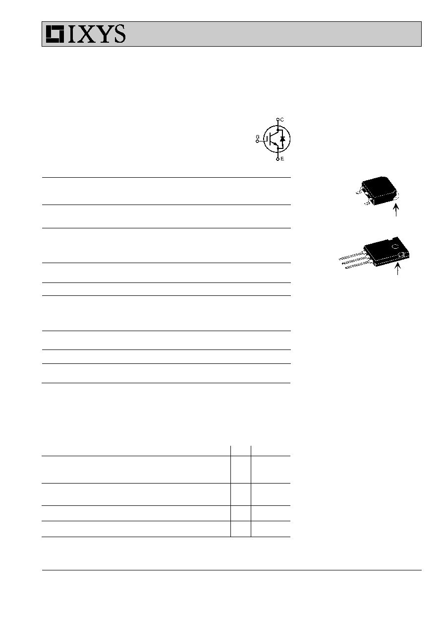
C (TAB)
G = Gate,
C = Collector,
E = Emitter,
TAB = Collector
G
C
E
TO-247 AD
(IXGH)
98510C (7/00)
Symbol
Test Conditions
Characteristic Values
(T
J
= 25
∞
C, unless otherwise specified)
min.
typ.
max.
BV
CES
I
C
= 250
m
A, V
GE
= 0 V
600
V
V
GE(th)
I
C
= 250
m
A, V
CE
= V
GE
2.5
5.0
V
I
CES
V
CE
= 0.8 ∑ V
CES
T
J
= 25
∞
C
200
m
A
V
GE
= 0 V
T
J
= 150
∞
C
3
mA
I
GES
V
CE
= 0 V, V
GE
=
±
20 V
±
100
nA
V
CE(sat)
I
C
= I
C90
, V
GE
= 15 V
1.8
V
Symbol
Test Conditions
Maximum Ratings
V
CES
T
J
= 25
∞
C to 150
∞
C
600
V
V
CGR
T
J
= 25
∞
C to 150
∞
C; R
GE
= 1 M
W
600
V
V
GES
Continuous
±
20
V
V
GEM
Transient
±
30
V
I
C25
T
C
= 25
∞
C
60
A
I
C90
T
C
= 90
∞
C
30
A
I
CM
T
C
= 25
∞
C, 1 ms
120
A
SSOA
V
GE
= 15 V, T
VJ
= 125
∞
C, R
G
= 10
W
I
CM
= 60
A
(RBSOA)
Clamped inductive load, L = 100
m
H
@ 0.8 V
CES
P
C
T
C
= 25
∞
C
200
W
T
J
-55 ... +150
∞
C
T
JM
150
∞
C
T
stg
-55 ... +150
∞
C
Maximum Lead and Tab temperature for soldering
300
∞
C
1.6 mm (0.062 in.) from case for 10 s
M
d
Mounting torque, TO-247 AD
1.13/10
Nm/lb.in.
Weight
TO-247 AD
6
g
TO-268
4
g
HiPerFAST
TM
IGBT
with Diode
TO-268
(IXGT)
G
E
C (TAB)
Features
∑ International standard package
∑ Moderate frequency IGBT and
antiparallel FRED in one package
∑ High current handling capability
∑ Newest generation HDMOS
TM
process
∑ MOS Gate turn-on
- drive simplicity
Applications
∑ AC motor speed control
∑ DC servo and robot drives
∑ DC choppers
∑ Uninterruptible power supplies (UPS)
∑ Switch-mode and resonant-mode
power supplies
Advantages
∑ Space savings (two devices in one
package)
∑ High power density
∑ Optimized V
ce(sat)
and switching
speeds for medium frequency
application
V
CES
=
600 V
I
C25
=
60 A
V
CE(sat)
=
1.8 V
t
fi(typ)
= 100 ns
IXYS reserves the right to change limits, test conditions, and dimensions.
IXGH 30N60BD1
IXGT 30N60BD1

2 - 5
© 2000 IXYS All rights reserved
Symbol
Test Conditions
Characteristic Values
(T
J
= 25
∞
C, unless otherwise specified)
min.
typ.
max.
g
fs
I
C
= I
C90
; V
CE
= 10 V,
25
S
Pulse test, t
£
300
m
s, duty cycle
£
2 %
C
ies
2700
pF
C
oes
V
CE
= 25 V, V
GE
= 0 V, f = 1 MHz
240
pF
C
res
50
pF
Q
g
110
nC
Q
ge
I
C
= I
C90
, V
GE
= 15 V, V
CE
= 0.5 V
CES
22
nC
Q
gc
40
nC
t
d(on)
25
ns
t
ri
30
ns
t
d(off)
130
220
ns
t
fi
100
190
ns
E
off
1.0
2.0
mJ
t
d(on)
25
ns
t
ri
35
ns
E
on
1.0
mJ
t
d(off)
200
ns
t
fi
230
ns
E
off
2.5
mJ
R
thJC
0.62 K/W
R
thCK
(TO-247 AD)
0.25
K/W
Reverse Diode (FRED)
Characteristic Values
(T
J
= 25
∞
C, unless otherwise specified)
Symbol
Test Conditions
min.
typ.
max.
V
F
I
F
= I
C90
, V
GE
= 0 V, Pulse test
T
J
= 150
∞
C
1.6
V
t
£
300
m
s, duty cycle d
£
2 %
2.5
V
I
RM
I
F
= I
C90
, V
GE
= 0 V, -di
F
/dt = 100 A/
m
s
6
A
t
rr
V
R
= 100 V
T
J
=100
∞
C
100
ns
I
F
= 1 A; -di/dt = 100 A/
m
s; V
R
= 30 V
25
ns
R
thJC
0.9 K/W
Inductive load, T
J
= 25
∞
C
I
C
= I
C90
, V
GE
= 15 V, L = 100
m
H,
V
CE
= 0.8 V
CES
, R
G
= R
off
= 4.7
W
Remarks: Switching times may
increase for V
CE
(Clamp) > 0.8 ∑ V
CES
,
higher T
J
or increased R
G
Inductive load, T
J
= 150
∞
C
I
C
= I
C90
, V
GE
= 15 V, L = 100
m
H
V
CE
= 0.8 V
CES
, R
G
= R
off
= 4.7
W
Remarks: Switching times may
increase for V
CE
(Clamp) > 0.8 ∑ V
CES
,
higher T
J
or increased R
G
IXGH 30N60BD1
IXGT 30N60BD1
TO-247 AD (IXGH) Outline
Dim. Millimeter
Inches
Min.
Max.
Min.
Max.
A
19.81 20.32
0.780 0.800
B
20.80 21.46
0.819 0.845
C
15.75 16.26
0.610 0.640
D
3.55
3.65
0.140 0.144
E
4.32
5.49
0.170 0.216
F
5.4
6.2
0.212 0.244
G
1.65
2.13
0.065 0.084
H
-
4.5
-
0.177
J
1.0
1.4
0.040 0.055
K
10.8
11.0
0.426 0.433
L
4.7
5.3
0.185 0.209
M
0.4
0.8
0.016 0.031
N
1.5
2.49
0.087 0.102
TO-268AA (D
3
PAK)
Dim.
Millimeter
Inches
Min.
Max.
Min.
Max.
A
4.9
5.1
.193
.201
A
1
2.7
2.9
.106
.114
A
2
.02
.25
.001
.010
b
1.15
1.45
.045
.057
b
2
1.9
2.1
.75
.83
C
.4
.65
.016
.026
D
13.80
14.00
.543
.551
E
15.85
16.05
.624
.632
E
1
13.3
13.6
.524
.535
e 5.45 BSC .215 BSC
H
18.70
19.10
.736
.752
L
2.40
2.70
.094
.106
L1
1.20
1.40
.047
.055
L2
1.00
1.15
.039
.045
L3 0.25 BSC .010 BSC
L4
3.80
4.10
.150
.161
Min. Recommended Footprint
IXYS MOSFETS and IGBTs are covered by one or more of the following U.S. patents:
4,835,592
4,881,106
5,017,508
5,049,961
5,187,117
5,486,715
4,850,072
4,931,844
5,034,796
5,063,307
5,237,481
5,381,025

3 - 5
© 2000 IXYS All rights reserved
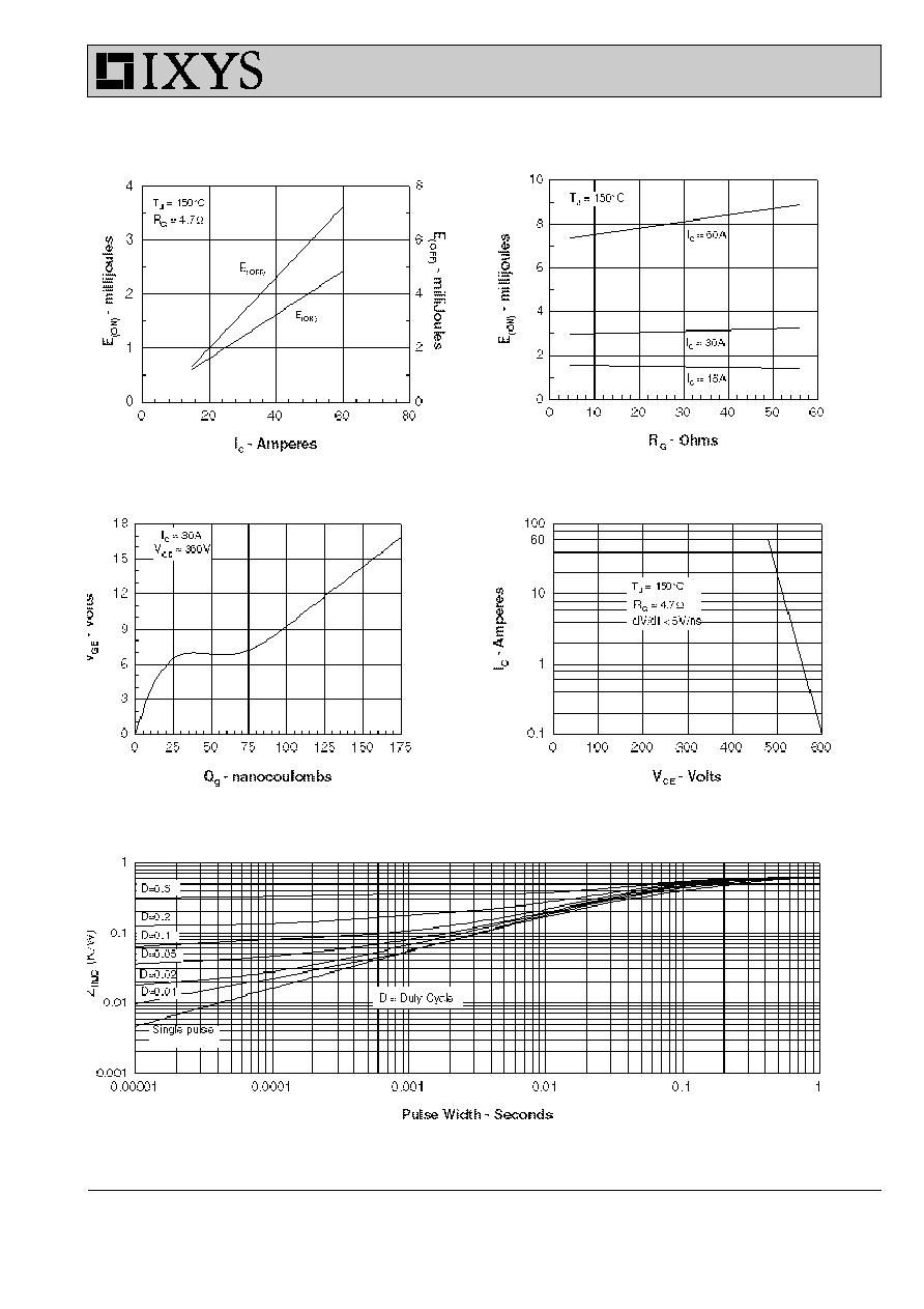
Fig. 1. Saturation Voltage Characteristics
Fig. 2. Extended Output Characteristics
Fig. 3. Saturation Voltage Characteristics
Fig. 4. Temperature Dependence of V
CE(sat)
Fig. 5. Admittance Curves
Fig. 6.Temperature Dependence of
BV
DSS
& V
GE(th)
IXGH 30N60BD1
IXGT 30N60BD1
4 - 5
© 2000 IXYS All rights reserved
Fig. 7. Dependence of E
OFF
and E
OFF
on I
C
.
Fig. 8. Dependence of E
OFF
on R
G
.
Fig. 9. Gate Charge
Fig. 10. Turn-off Safe Operating Area
Fig. 11. IGBT Transient Thermal
Resistance
IXGH 30N60BD1
IXGT 30N60BD1
5 - 5
© 2000 IXYS All rights reserved
IXGH 30N60BD1
IXGT 30N60BD1
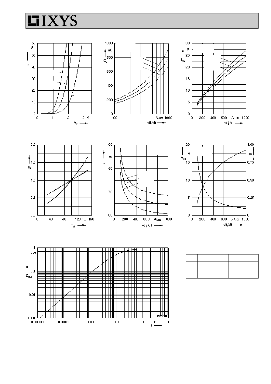
I
F
= 60A
I
F
= 30A
I
F
= 15A
T
VJ
= 100∞C
V
R
= 300V
T
VJ
= 100∞C
I
F
= 30A
Fig. 14 Peak reverse current I
RM
versus -di
F
/dt
Fig. 13 Reverse recovery charge Q
r
versus -di
F
/dt
Fig. 12 Forward current I
F
versus V
F
T
VJ
= 100∞C
V
R
= 300V
T
VJ
= 100∞C
V
R
= 300V
I
F
= 60A
I
F
= 30A
I
F
= 15A
Q
r
I
RM
Fig. 15 Dynamic parameters Q
r
, I
RM
versus T
VJ
Fig. 16 Recovery time t
rr
versus -di
F
/dt
Fig. 17 Peak forward voltage V
FR
and t
fr
versus di
F
/dt
I
F
= 60A
I
F
= 30A
I
F
= 15A
t
fr
V
FR
Fig. 18 Transient thermal resistance junction to case
Constants for Z
thJC
calculation:
i
R
thi
(K/W)
t
i
(s)
1
0.502
0.0052
2
0.193
0.0003
3
0.205
0.0162
T
VJ
=25∞C
T
VJ
=100∞C
T
VJ
=150∞C