 | –≠–ª–µ–∫—Ç—Ä–æ–Ω–Ω—ã–π –∫–æ–º–ø–æ–Ω–µ–Ω—Ç: 32N60CD1 | –°–∫–∞—á–∞—Ç—å:  PDF PDF  ZIP ZIP |
© 2002 IXYS All rights reserved
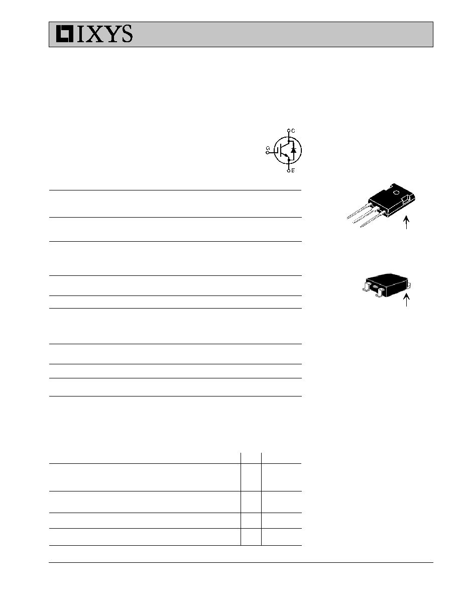
G
C
E
TO-247 AD (IXGH)
97544E (6/02)
Symbol
Test Conditions
Characteristic Values
(T
J
= 25
∞
C, unless otherwise specified)
min.
typ.
max.
BV
CES
I
C
= 250
µ
A, V
GE
= 0 V
600
V
V
GE(th)
I
C
= 250
µ
A, V
CE
= V
GE
2.5
5.0
V
I
CES
V
CE
= 0.8 ∑ V
CES
T
J
= 25
∞
C
200
µ
A
V
GE
= 0 V
T
J
= 125
∞
C
3
mA
I
GES
V
CE
= 0 V, V
GE
=
±
20 V
±
100
nA
V
CE(sat)
I
C
= I
C90
, V
GE
= 15 V
2.1
2.5
V
Symbol
Test Conditions
Maximum Ratings
V
CES
T
J
= 25
∞
C to 150
∞
C
600
V
V
CGR
T
J
= 25
∞
C to 150
∞
C; R
GE
= 1 M
600
V
V
GES
Continuous
±
20
V
V
GEM
Transient
±
30
V
I
C25
T
C
= 25
∞
C
60
A
I
C90
T
C
= 90
∞
C
32
A
I
CM
T
C
= 25
∞
C, 1 ms
120
A
SSOA
V
GE
= 15 V, T
VJ
= 125
∞
C, R
G
= 10
I
CM
= 64
A
(RBSOA)
Clamped inductive load @ 0.8 V
CES
P
C
T
C
= 25
∞
C
200
W
T
J
-55 ... +150
∞
C
T
JM
150
∞
C
T
stg
-55 ... +150
∞
C
Maximum Lead and Tab temperature for soldering
300
∞
C
1.6 mm (0.062 in.) from case for 10 s
M
d
Mounting torque, TO-247 AD
1.13/10
Nm/lb.in.
Weight
TO-247 AD
6
g
TO-268
5
g
HiPerFAST
TM
IGBT
with Diode
Light Speed Series
Features
International standard TO-247AD
package
High current handling capability
Latest generation HDMOS
TM
process
MOS Gate turn-on
- drive simplicity
Applications
Uninterruptible power supplies (UPS)
Switched-mode and resonant-mode
power supplies
AC motor speed control
DC servo and robot drives
DC choppers
Advantages
High power density
Very fast switching speeds for high
frequency applications
High power surface mountable package
IXGH 32N60CD1
IXGT 32N60CD1
V
CES
= 600 V
I
C25
= 60 A
V
CE(SAT)typ
= 2.1 V
t
fi(typ)
= 55 ns
G = Gate
C = Collector
E = Emitter
TO-268 (D3) ( IXGT)
C (TAB)
G
E
C (TAB)
IXYS reserves the right to change limits, test conditions, and dimensions.
IXYS MOSFETs and IGBTs are covered by one or more of the following U.S. patents:
4,835,592
4,881,106
5,017,508
5,049,961
5,187,117
5,486,715
6,306,728B1
4,850,072
4,931,844
5,034,796
5,063,307
5,237,481
5,381,025
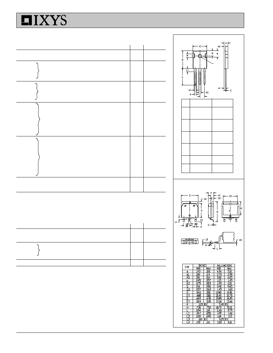
TO-247 AD Outline
Dim.
Millimeter
Inches
Min.
Max.
Min. Max.
A
4.7
5.3
.185
.209
A
1
2.2
2.54
.087
.102
A
2
2.2
2.6
.059
.098
b
1.0
1.4
.040
.055
b
1
1.65
2.13
.065
.084
b
2
2.87
3.12
.113
.123
C
.4
.8
.016
.031
D
20.80
21.46
.819
.845
E
15.75
16.26
.610
.640
e
5.20
5.72
0.205 0.225
L
19.81
20.32
.780
.800
L1
4.50
.177
P
3.55
3.65
.140
.144
Q
5.89
6.40
0.232 0.252
R
4.32
5.49
.170
.216
S
6.15 BSC
242 BSC
e
P
Symbol
Test Conditions
Characteristic Values
(T
J
= 25
∞
C, unless otherwise specified)
min.
typ.
max.
g
fs
I
C
= I
C90
; V
CE
= 10 V,
25
S
Pulse test, t
300
µ
s, duty cycle
2 %
C
ies
2700
pF
C
oes
V
CE
= 25 V, V
GE
= 0 V, f = 1 MHz
240
pF
C
res
50
pF
Q
g
110
nC
Q
ge
I
C
= I
C90
, V
GE
= 15 V, V
CE
= 0.5 V
CES
22
nC
Q
gc
40
nC
t
d(on)
25
ns
t
ri
20
ns
t
d(off)
85
ns
t
fi
55
ns
E
off
0.32
mJ
t
d(on)
25
ns
t
ri
25
ns
E
on
1
mJ
t
d(off)
110
170
ns
t
fi
100
160
ns
E
off
0.85
1.25 mJ
R
thJC
0.62 K/W
R
thCK
0.25
K/W
Reverse Diode (FRED)
Characteristic Values
(T
J
= 25
∞
C, unless otherwise specified)
Symbol
Test Conditions
min.
typ.
max.
V
F
I
F
= I
C90
, V
GE
= 0 V, Pulse test T
J
=150
∞
C
1.6
V
t
300
µ
s, duty cycle d
2 % T
J
= 25
∞
C
2.5
V
I
RM
I
F
= I
C90
, V
GE
= 0 V, -di
F
/dt = 100 A/
µ
s
6
A
t
rr
V
R
= 100 V
T
J
= 100
∞
C 100
ns
I
F
= 1 A; -di/dt = 100 A/
µ
s; V
R
= 30 V T
J
= 25
∞
C
25
ns
R
thJC
0.9 K/W
Inductive load, T
J
= 25
∞∞
∞∞
∞
C
I
C
= I
C90
, V
GE
= 15 V
V
CE
= 0.8 V
CES
, R
G
= R
off
= 4.7
Remarks: Switching times may
increase for V
CE
(Clamp) > 0.8 ∑ V
CES
,
higher T
J
or increased R
G
Inductive load, T
J
= 125
∞∞
∞∞
∞
C
I
C
= I
C90
, V
GE
= 15 V
V
CE
= 0.8 V
CES
, R
G
= R
off
= 4.7
Remarks: Switching times may
increase for V
CE
(Clamp) > 0.8 ∑ V
CES
,
higher T
J
or increased R
G
IXGH 32N60CD1
IXGT 32N60CD1
TO-268 Outline
Terminals: 1 - Gate
2 - Collector
3 - Emitter
© 2002 IXYS All rights reserved
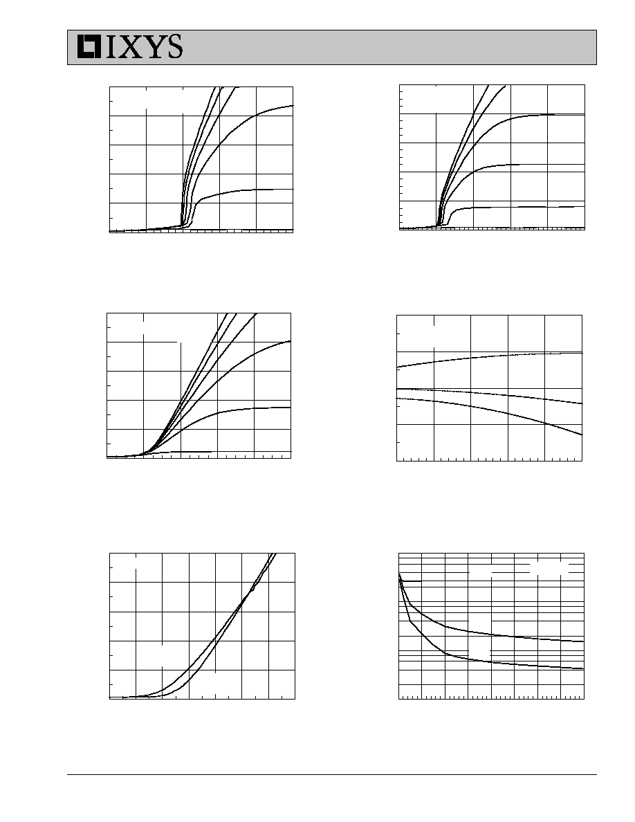
V
CE
- Volts
0
1
2
3
4
5
I
C
- A
m
p
e
re
s
0
20
40
60
80
100
V
CE
- Volts
0
1
2
3
4
5
I
C
- Am
p
e
re
s
0
20
40
60
80
100
V
CE
-Volts
0
5
10
15
20
25
30
35
40
C
a
p
a
ci
t
a
n
ce -
p
F
10
100
1000
10000
T
J
- Degrees C
25
50
75
100
125
150
V
CE
(
s
a
t
)
- N
o
rm
a
l
iz
e
d
0.50
0.75
1.00
1.25
1.50
V
GE
- Volts
3
4
5
6
7
8
9
10
I
C
- Am
p
e
re
s
0
20
40
60
80
100
V
CE
- Volts
0
2
4
6
8
10
I
C
- Am
p
e
re
s
0
40
80
120
160
200
13V
11V
9V
7V
V
CE
= 10V
V
GE
= 15V
13V
T
J
= 25∞C
V
GE
= 15V
T
J
= 25∞C
I
C
= 16A
I
C
= 32A
I
C
= 64A
T
J
=
125∞C
f = 1Mhz
5V
5V
V
GE
= 15V
T
J
= 25∞C
T
J
= 125∞C
7V
9V
5V
7V
9V
V
GE
= 15V
13V
C
iss
C
oss
C
rss
11V
11V
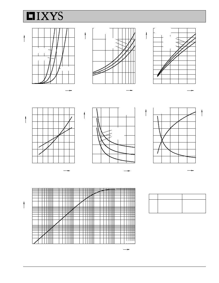
Fig. 1. Output Characteristics
Fig. 2. Extended Output Characteristics
Fig. 3. High Temperature Output Characteristics
Fig. 4. Temperature Dependence of V
CE(sat)
Fig. 5. Admittance Curves
Fig. 6. Capacitance Curves
IXGH 32N60CD1
IXGT 32N60CD1
IXYS reserves the right to change limits, test conditions, and dimensions.
IXYS MOSFETs and IGBTs are covered by one or more of the following U.S. patents:
4,835,592
4,881,106
5,017,508
5,049,961
5,187,117
5,486,715
6,306,728B1
4,850,072
4,931,844
5,034,796
5,063,307
5,237,481
5,381,025
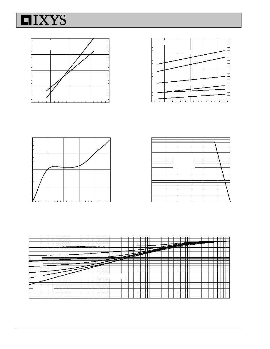
Pulse Width - Seconds
0.00001
0.0001
0.001
0.01
0.1
1
Z
thJ
C
(K/W)
0.001
0.01
0.1
1
D=0.2
V
CE
- Volts
0
100
200
300
400
500
600
I
C
-
A
m
pe
r
e
s
0.1
1
10
100
Q
g
- nanocoulombs
0
25
50
75
100
125
V
GE
-
V
o
lt
s
0
4
8
12
16
R
G
- Ohms
0
10
20
30
40
50
60
E
(O
FF)
- m
illijoule
s
0
2
4
6
8
E
(O
N
)
- millijou
l
es
0
1
2
3
4
I
C
- Amperes
0
20
40
60
80
E
(O
FF)
- milliJ
oule
s
0
1
2
3
4
E
(O
N
)
-
m
illij
ou
l
es
0.00
0.25
0.50
0.75
1.00
V
CE
= 300V
I
C
= 16A
I
C
= 32A
E
(ON)
E
(OFF)
E
(OFF)
T
J
= 125∞C
R
G
= 4.7
dV/dt < 5V/ns
D=0.5
D=0.1
D=0.05
D=0.02
D=0.01
Single pulse
D = Duty Cycle
R
G
= 10
T
J
= 125∞C
64
E
(ON)
I
C
= 64A
E
(OFF)
T
J
= 125∞C
E
(ON)
I
C
= 32A
E
(ON)
E
(OFF)
Fig. 7. Dependence of E
ON
and E
OFF
on I
C
.
Fig. 8. Dependence of E
ON
and E
OFF
on R
G
.
Fig. 9. Gate Charge
Fig. 10. Turn-off Safe Operating Area
Fig. 11. Transient Thermal Resistance
IXGH 32N60CD1
IXGT 32N60CD1
© 2002 IXYS All rights reserved
200
600
1000
0
400
800
60
70
80
90
0.00001
0.0001
0.001
0.01
0.1
1
0.001
0.01
0.1
1
0
40
80
120
160
0.0
0.5
1.0
1.5
2.0
K
f
T
VJ
∞C
-di
F
/dt
t
s
K/W
0
200
400
600
800 1000
0
5
10
15
20
0.00
0.25
0.50
0.75
1.00
V
FR
di
F
/dt
V
200
600
1000
0
400
800
0
5
10
15
20
25
30
100
1000
0
200
400
600
800
1000
0
1
2
3
0
10
20
30
40
50
60
I
RM
Q
r
I
F
A
V
F
-di
F
/dt
-di
F
/dt
A/
µ
s
A
V
nC
A/
µ
s
A/
µ
s
t
rr
ns
t
fr
Z
thJC
A/
µ
s
µ
s
DSEP 29-06
I
F
= 60A
I
F
= 30A
I
F
= 15A
T
VJ
= 100∞C
V
R
= 300V
T
VJ
= 100∞C
I
F
= 30A
Fig. 14 Peak reverse current I
RM
versus -di
F
/dt
Fig. 13 Reverse recovery charge Q
r
versus -di
F
/dt
Fig. 12 Forward current I
F
versus V
F
T
VJ
= 100∞C
V
R
= 300V
T
VJ
= 100∞C
V
R
= 300V
I
F
= 60A
I
F
= 30A
I
F
= 15A
Q
r
I
RM
Fig. 15 Dynamic parameters Q
r
, I
RM
versus T
VJ
Fig. 16 Recovery time t
rr
versus -di
F
/dt
Fig. 17 Peak forward voltage V
FR
and
t
fr
versus di
F
/dt
I
F
= 60A
I
F
= 30A
I
F
= 15A
t
fr
V
FR
Fig. 18 Transient thermal resistance junction to case
Constants for Z
thJC
calculation:
i
R
thi
(K/W)
t
i
(s)
1
0.502
0.0052
2
0.193
0.0003
3
0.205
0.0162
T
VJ
=25∞C
T
VJ
=100∞C
T
VJ
=150∞C
IXGH 32N60CD1
IXGT 32N60CD1