1 - 4
© 2000 IXYS All rights reserved
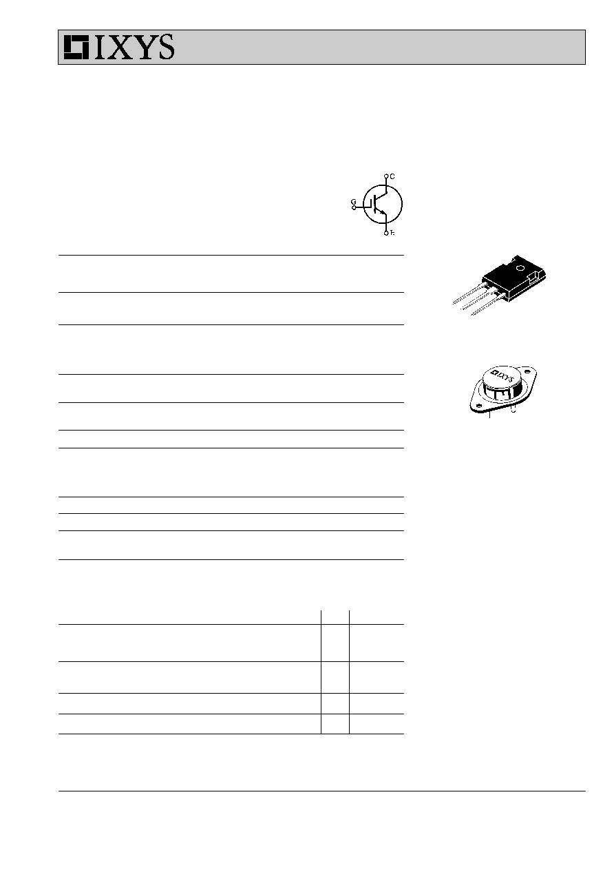
TO-247 AD (IXSH)
G
C
E
Symbol
Test Conditions
Maximum Ratings
V
CES
T
J
= 25
∞
C to 150
∞
C
1000
V
V
CGR
T
J
= 25
∞
C to 150
∞
C; R
GE
= 1 M
W
1000
V
V
GES
Continuous
±
20
V
V
GEM
Transient
±
30
V
I
C25
T
C
= 25
∞
C
70
A
I
C90
T
C
= 90
∞
C
35
A
I
CM
T
C
= 25
∞
C, 1 ms
140
A
SSOA
V
GE
= 15 V, T
J
= 125
∞
C, R
G
= 2.7
W
I
CM
= 70
A
(RBSOA)
Clamped inductive load, L = 30
m
H
@ 0.8 V
CES
t
SC
V
GE
= 15 V, V
CE
= 0.6 ∑ V
CES
, T
J
= 125
∞
C
10
m
s
(SCSOA)
R
G
= 22
W,
non repetitive
P
C
T
C
= 25
∞
C
300
W
T
J
-55 ... +150
∞
C
T
JM
150
∞
C
T
stg
-55 ... +150
∞
C
M
d
Mounting torque
1.13/10
Nm/lb.in.
Weight
TO-204 = 18 g, TO-247 = 6 g
Maximum lead temperature for soldering
300
∞
C
1.6 mm (0.062 in.) from case for 10 s
TO-204 AE (IXSM)
C
G = Gate,
C = Collector,
E = Emitter,
TAB = Collector
Features
q
International standard packages
q
Guaranteed Short Circuit SOA
capability
q
Low V
CE(sat)
- for low on-state conduction losses
q
High current handling capability
q
MOS Gate turn-on
- drive simplicity
q
Fast Fall Time for switching speeds
up to 20 kHz
Applications
q
AC motor speed control
q
Uninterruptible power supplies (UPS)
q
Welding
Advantages
q
Easy to mount with 1 screw (TO-247)
(isolated mounting screw hole)
q
High power density
High speed IGBT
IXSH 35N100A
V
CES
= 1000 V
IXSM 35N100A
I
C25
= 70 A
V
CE(sat)
= 3.5 V
Short Circuit SOA Capability
Symbol
Test Conditions
Characteristic Values
(T
J
= 25
∞
C, unless otherwise specified)
min.
typ.
max.
BV
CES
I
C
= 3 mA, V
GE
= 0 V
1000
V
V
GE(th)
I
C
= 4 mA, V
CE
= V
GE
5
8
V
I
CES
V
CE
= 0.8 ∑ V
CES
T
J
= 25
∞
C
250
m
A
V
GE
= 0 V
T
J
= 125
∞
C
1
mA
I
GES
V
CE
= 0 V, V
GE
=
±
20 V
±
100
nA
V
CE(sat)
I
C
= I
C90
, V
GE
= 15 V
3.5
V
91545F (12/96)
IXYS reserves the right to change limits, test conditions, and dimensions.
2 - 4
© 2000 IXYS All rights reserved
Symbol
Test Conditions
Characteristic Values
(T
J
= 25
∞
C, unless otherwise specified)
min.
typ.
max.
g
fs
I
C
= I
C90
; V
CE
= 10 V,
20
25
S
Pulse test, t
£
300
m
s, duty cycle d
£
2 %
I
C(on)
V
GE
= 15 V, V
CE
= 10 V
240
A
C
ies
4400
pF
C
oes
V
CE
= 25 V, V
GE
= 0 V, f = 1 MHz
325
pF
C
res
85
pF
Q
g
180
260
nC
Q
ge
I
C
= I
C90
, V
GE
= 15 V, V
CE
= 0.5 V
CES
45
60
nC
Q
gc
120
200
nC
t
d(on)
80
ns
t
ri
150
ns
t
d(off)
400
ns
t
fi
700
950
ns
E
off
10
mJ
t
d(on)
100
ns
t
ri
200
ns
E
on
4.2
mJ
t
d(off)
400
550
ns
t
fi
1300
2000
ns
E
off
15
31
mJ
R
thJC
0.42 K/W
R
thCK
0.25
K/W
Inductive load, T
J
= 25
∞
C
I
C
= I
C90
, V
GE
= 15 V, L = 100
m
H
V
CE
= 0.8 V
CES
, R
G
= 2.7
W
Switching times may increase for
V
CE
(Clamp) > 0.8 ∑ V
CES
, higher T
J
or increased R
G
Inductive load, T
J
= 125
∞
C
I
C
= I
C90
, V
GE
= 15 V, L = 100
m
H
V
CE
= 0.8 V
CES
, R
G
= 2.7
W
Remarks: Switching times
may increase for
V
CE
(Clamp) > 0.8 ∑ V
CES
, higher T
J
or
increased R
G
IXSH 35N100A
IXSM 35N100A
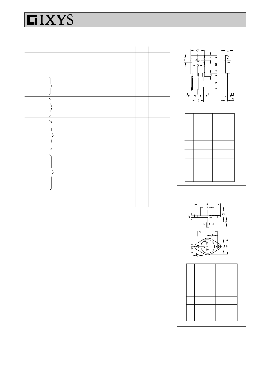
TO-247 AD (IXSH) Outline
Dim. Millimeter
Inches
Min.
Max.
Min.
Max.
A
19.81 20.32
0.780 0.800
B
20.80 21.46
0.819 0.845
C
15.75 16.26
0.610 0.640
D
3.55
3.65
0.140 0.144
E
4.32
5.49
0.170 0.216
F
5.4
6.2
0.212 0.244
G
1.65
2.13
0.065 0.084
H
-
4.5
-
0.177
J
1.0
1.4
0.040 0.055
K
10.8
11.0
0.426 0.433
L
4.7
5.3
0.185 0.209
M
0.4
0.8
0.016 0.031
N
1.5
2.49
0.087 0.102
TO-204 AE (IXSM) Outline
Dim.
Millimeter
Inches
Min.
Max.
Min.
Max.
A
38.61 39.12
1.520 1.540
B
- 22.22
- 0.875
C
6.40 11.40
0.252 0.449
D
1.45
1.60
0.057 0.063
E
1.52
3.43
0.060 0.135
F
30.15
BSC
1.187
BSC
G
10.67 11.17
0.420 0.440
H
5.21
5.71
0.205 0.225
J
16.64 17.14
0.655 0.675
K
11.18 12.19
0.440 0.480
Q
3.84
4.19
0.151 0.165
R
25.16 26.66
0.991 1.050
IXYS MOSFETS and IGBTs are covered by one or more of the following U.S. patents:
4,835,592
4,881,106
5,017,508
5,049,961
5,187,117
5,486,715
4,850,072
4,931,844
5,034,796
5,063,307
5,237,481
5,381,025

3 - 4
© 2000 IXYS All rights reserved
T
J
- Degrees C
-50
-25
0
25
50
75
100 125 150
BV /
V
GE
(
t
h
)
- N
o
rm
a
liz
e
d
0.7
0.8
0.9
1.0
1.1
1.2
1.3
BV
CES
I
C
= 3mA
V
GE
- Volts
4
5
6
7
8
9
10 11 12 13 14 15
I
C
-
Am
per
es
0
10
20
30
40
50
V
CE
= 10V
T
J
- Degrees C
-50
-25
0
25
50
75
100 125 150
V
CE
(
s
at
)
- N
o
rm
a
liz
e
d
0.7
0.8
0.9
1.0
1.1
1.2
1.3
1.4
V
GE
=15V
V
GE
- Volts
8
9
10
11
12
13
14
15
V
CE
- V
o
lts
0
1
2
3
4
5
6
7
8
9
10
T
J
= 25∞C
V
CE
- Volts
0
2
4
6
8
10 12 14 16 18 20
I
C
-
Am
per
es
0
50
100
150
200
250
T
J
= 25∞C
7V
9V
11V
13V
V
CE
- Volts
0
1
2
3
4
5
I
C
-
Am
per
es
0
10
20
30
40
50
60
70
T
J
= 25∞C
V
GE
=15V
11V
7V
9V
V
GE(th)
I
C
= 4mA
13V
V
GE
= 15V
I
C
= 17.5A
I
C
= 35A
I
C
= 70A
T
J
= - 40C
T
J
= 25∞C
T
J
= 125∞C
I
C
=1 7.5A
I
C
= 35A
I
C
= 70A
Fig.3 Collector-Emitter Voltage
Fig.4
Temperature Dependence
vs. Gate-Emitter Voltage
of Output Saturation Voltage
Fig.5 Input Admittance
Fig.6 Temperature Dependence of
Breakdown and Threshold Voltage
Fig.1 Saturation Characteristics
Fig.2
Output Characterstics
IXSH 35N100A
IXSM 35N100A

4 - 4
© 2000 IXYS All rights reserved
Pulse Width - Seconds
0.00001
0.0001
0.001
0.01
0.1
1
10
Z
th
J
C
-
K
/
W
0.001
0.01
0.1
1
Single Pulse
D=0.2
V
CE
- Volts
0
200
400
600
800
1000
I
C
-
Am
per
es
0.01
0.1
1
10
100
T
J
= 125∞C
R
G
= 2.7
W
dV/dt < 5V/ns
Q
g
- nanocoulombs
0
50
100
150
200
V
GE
- V
o
l
t
s
0
3
6
9
12
15
R
G
- Ohms
0
10
20
30
40
50
E
of
f
-
m
i
llij
o
u
l
e
s
14
15
16
17
18
t
fi
-
nanoseconds
1000
1250
1500
1750
2000
t
fi
E
off
I
C
- Amperes
0
10
20
30
40
50
60
70
E
of
f
-
m
i
llij
o
u
l
e
s
5
10
15
20
25
t
fi
-
nanoseconds
1000
1250
1500
1750
2000
E
off
t
fi
D = Duty Cycle
T
J
= 125∞C
R
G
= 10
W
T
J
= 125∞C
I
C
= 35A
I
C
= 35A
V
CE
= 500V
D=0.5
D=0.01
D=0.02
D=0.05
D=0.1
Fig.11 Transient Thermal Impedance
Fig.9 Gate Charge Characteristic Curve
Fig.10 Turn-Off Safe Operating Area
Fig.7 Turn-Off Energy per Pulse and
Fig.8 Dependence of Turn-Off Energy
Fall Time on Collector Current
Per Pulse and Fall Time on R
G
IXSH 35N100A
IXSM 35N100A