 | –≠–ª–µ–∫—Ç—Ä–æ–Ω–Ω—ã–π –∫–æ–º–ø–æ–Ω–µ–Ω—Ç: 40N60A | –°–∫–∞—á–∞—Ç—å:  PDF PDF  ZIP ZIP |

IXYS Corporation
3540 Bassett Street, Santa Clara CA 95054
Phone: 408-982-0700, Fax: 408-496-0670
IXYS Semiconductor GmbH
Edisonstr. 15, D-68623 Lampertheim
Phone: +49-6206-503-0, Fax: +49-6206-503627
© IXYS Corporation. All rights reserved.
TO-247 AD (IXSH)
V
CES
I
C25
V
CE(sat)
Low V
CE(sat)
IGBT
IXSH/IXSM
40
N60
600 V
75 A
2.5 V
High Speed IGBT
IXSH/IXSM
40
N60A
600 V
75 A
3.0 V
Short Circuit SOA Capability
G
C
E
Symbol
Test Conditions
Maximum Ratings
V
CES
T
J
= 25
∞
C to 150
∞
C
600
V
V
CGR
T
J
= 25
∞
C to 150
∞
C; R
GE
= 1 M
600
V
V
GES
Continuous
±
20
V
V
GEM
Transient
±
30
V
I
C25
T
C
= 25
∞
C
75
A
I
C90
T
C
= 90
∞
C
40
A
I
CM
T
C
= 25
∞
C, 1 ms
150
A
SSOA
V
GE
= 15 V, T
J
= 125
∞
C, R
G
= 2.7
I
CM
= 80
A
(RBSOA)
Clamped inductive load, L = 30
µ
H
@ 0.8 V
CES
t
SC
V
GE
= 15 V, V
CE
= 360 V, T
J
= 125
∞
C
10
µ
s
(SCSOA)
R
G
= 22
,
non repetitive
P
C
T
C
= 25
∞
C
300
W
T
J
-55 ... +150
∞
C
T
JM
150
∞
C
T
stg
-55 ... +150
∞
C
M
d
Mounting torque
1.13/10 Nm/lb.in.
Weight
TO-204 = 18 g, TO-247 = 6g
Maximum lead temperature for soldering
300
∞
C
1.6 mm (0.062 in.) from case for 10 s
Symbol
Test Conditions
Characteristic Values
(T
J
= 25
∞
C, unless otherwise specified)
min.
typ.
max.
BV
CES
I
C
= 250
µ
A, V
GE
= 0 V
600
V
V
GE(th)
I
C
= 4 mA, V
CE
= V
GE
4
7
V
I
CES
V
CE
= 0.8 ∑ V
CES
T
J
= 25
∞
C
50
µ
A
V
GE
= 0 V
T
J
= 125
∞
C
1
mA
I
GES
V
CE
= 0 V, V
GE
=
±
20 V
±
100
nA
V
CE(sat)
I
C
= I
C90
, V
GE
= 15 V
40N60
2.5
V
40N60A
3.0
V
TO-204 AE (IXSM)
C
G = Gate,
C = Collector,
E = Emitter,
TAB = Collector
Features
q
International standard packages
q
Guaranteed Short Circuit SOA
capability
q
Low V
CE(sat)
- for low on-state conduction losses
q
High current handling capability
q
MOS Gate turn-on
- drive simplicity
q
Fast Fall Time for switching speeds
up to 20 kHz
Applications
q
AC motor speed control
q
Uninterruptible power supplies (UPS)
q
Welding
Advantages
q
Easy to mount with 1 screw (TO-247)
(isolated mounting screw hole)
q
High power density
IXYS reserves the right to change limits, test conditions and dimensions.
91546F (4/96)

IXYS Semiconductor GmbH
Edisonstr. 15, D-68623 Lampertheim
Phone: +49-6206-503-0, Fax: +49-6206-503627
IXYS reserves the right to change limits, test conditions, and dimensions.
IXYS Corporation
3540 Bassett Street, Santa Clara CA 95054
Phone: 408-982-0700, Fax: 408-496-0670
IXSH 40N60
IXSM 40N60
IXSH 40N60A
IXSM 40N60A
TO-247 AD Outline
Symbol
Test Conditions
Characteristic Values
(T
J
= 25
∞
C, unless otherwise specified)
min.
typ.
max.
g
fs
I
C
= I
C90
; V
CE
= 10 V,
16
23
S
Pulse test, t
300
µ
s, duty cycle
2 %
I
C(on)
V
GE
= 15 V, V
CE
= 10 V
200
A
C
ies
4500
pF
C
oes
V
CE
= 25 V, V
GE
= 0 V, f = 1 MHz
350
pF
C
res
90
pF
Q
g
190
260
nC
Q
ge
I
C
= I
C90
, V
GE
= 15 V, V
CE
= 0.5 V
CES
45
60
nC
Q
gc
88
120
nC
t
d(on)
55
ns
t
ri
170
ns
t
d(off)
400
ns
t
fi
40N60
400
ns
40N60A
200
ns
E
off
40N60
5.0
mJ
40N60A
2.5
mJ
t
d(on)
55
ns
t
ri
170
ns
E
on
1.7
mJ
t
d(off)
40N60
1000
ns
40N60A
340
525
ns
t
fi
40N60
600
1500
ns
40N60A
340
700
ns
E
off
40N60
12
mJ
40N60A
6
mJ
R
thJC
0.42 K/W
R
thCK
0.25
K/W
TO-204AE Outline
1 = Gate
2 = Collector
3 = Emitter
Tab = Collector
1 = Gate
2 = Emitter
Case = Collector
Inductive load, T
J
= 25
∞∞
∞∞
∞
C
I
C
= I
C90
, V
GE
= 15 V, L = 100
µ
H
V
CE
= 0.8 V
CES
, R
G
= 2.7
Switching times may
increase for V
CE
(Clamp)
> 0.8 ∑ V
CES
, higher T
J
or
increased R
G
Inductive load, T
J
=
125
∞∞
∞∞
∞
C
I
C
= I
C90
, V
GE
= 15 V,
L = 100
µ
H
V
CE
= 0.8 V
CES
,
R
G
= 2.7
Remarks: Switching times
may increase for
V
CE
(Clamp) > 0.8 ∑ V
CES
,
higher T
J
or increased R
G
IXYS MOSFETs and IGBTs are covered by one of the following U.S.patents:
4,835,592 4,881,108 5,017,508 5,049,961 5,187,117 5,486,715
4,850,072 4,931,844 5,034,796 5,063,307 5,237,481 5,381,025
IXYS Corporation
3540 Bassett Street, Santa Clara CA 95054
Phone: 408-982-0700, Fax: 408-496-0670
IXYS Semiconductor GmbH
Edisonstr. 15, D-68623 Lampertheim
Phone: +49-6206-503-0, Fax: +49-6206-503627
© IXYS Corporation. All rights reserved.
IXSH 40N60
IXSM 40N60
IXSH 40N60A
IXSM 40N60A
T
J
- Degrees C
-50
-25
0
25
50
75
100 125
150
B
V
/ V
GE(th
)
- Norm
alized
0.7
0.8
0.9
1.0
1.1
1.2
1.3
BV
CES
I
C
= 3mA
V
GE
- Volts
4
5
6
7
8
9
10
11
12
13
I
C
-
Am
pe
res
0
10
20
30
40
50
60
70
80
T
J
- Degrees C
-50
-25
0
25
50
75
100 125
150
V
CE
(
s
at
)
-
Nor
ma
lize
d
0.7
0.8
0.9
1.0
1.1
1.2
1.3
1.4
1.5
V
GE
- Volts
8
9
10
11
12
13
14
15
V
CE
- V
olt
s
0
1
2
3
4
5
6
7
8
9
10
V
CE
- Volts
0
2
4
6
8
10
12
14
16
18
20
I
C
-
Am
pe
res
0
20
40
60
80
100
120
140
160
180
200
7V
9V
11V
13V
V
CE
- Volts
0
1
2
3
4
5
I
C
-
Am
pe
res
0
10
20
30
40
50
60
70
80
11V
7V
9V
13V
T
J
= 25∞C
V
GE
= 15V
T
J
= 25∞C
V
GE
= 15V
T
J
= 25∞C
I
C
= 20A
I
C
= 40A
I
C
= 80A
I
C
= 20A
I
C
= 40A
I
C
= 80A
V
GE
=15V
V
CE
= 10V
T
J
= 125∞C
T
J
= 25∞C
T
J
= - 40∞C
V
GE8th)
I
C
= 4mA
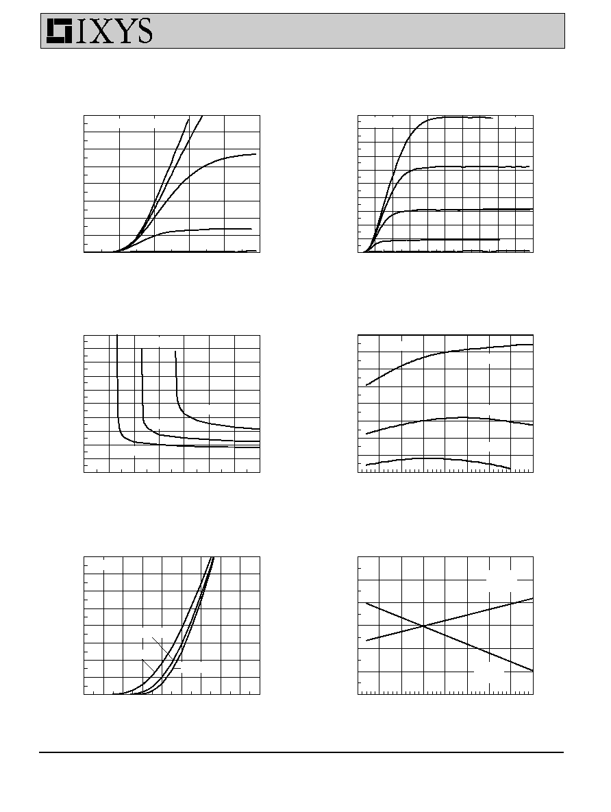
Fig. 3 Collector-Emitter Voltage
Fig. 4
Temperature Dependence
vs. Gate-Emitter Voltage
of Output Saturation Voltage
Fig. 5 Input Admittance
Fig. 6
Temperature Dependence of
Breakdown and
Threshold Voltage
Fig. 1 Saturation Characteristics
Fig. 2
Output Characterstics

IXYS Semiconductor GmbH
Edisonstr. 15, D-68623 Lampertheim
Phone: +49-6206-503-0, Fax: +49-6206-503627
IXYS reserves the right to change limits, test conditions, and dimensions.
IXYS Corporation
3540 Bassett Street, Santa Clara CA 95054
Phone: 408-982-0700, Fax: 408-496-0670
IXSH 40N60
IXSM 40N60
IXSH 40N60A
IXSM 40N60A
Time - Seconds
0.00001
0.0001
0.001
0.01
0.1
1
T
her
ma
l Re
sp
ons
e -
K/W
0.001
0.01
0.1
1
V
CE
- Volts
0
100
200
300
400
500
600
700
I
C
- A
m
per
es
0.01
0.1
1
10
100
T
J
= 125∞C
R
G
= 22
dV/dt < 6V/ns
Q
g
- nCoulombs
0
50
100
150
200
250
V
GE
-
Vo
lts
0
3
6
9
12
15
I
C
= 40A
V
CE
= 480V
R
G
- Ohms
0
10
20
30
40
50
0
2
4
6
8
10
tf
i - n
ano
se
con
ds
0
200
400
600
800
1000
I
C
- Amperes
0
10
20
30
40
50
60
70
80
T
fi
-
na
nos
ec
ond
s
0
250
500
750
1000
0
3
6
9
12
Single Pulse
D = Duty Cycle
D=0.01
D=0.5
D=0.2
D=0.02
E
of
f
-
m
illijo
ule
s
t
fi
(-A)
hi-speed
E
off
(-A)
hi-speed
T
J
= 125∞C
R
G
= 10
E
of
f
- m
illij
oul
es
t
fi
(-A), hi-speed
E
off
(-A), hi-speed
T
J
= 125∞C
I
C
= 40A
D=0.05
D=0.1
Fig.11 Transient Thermal Impedance
Fig.9 Gate Charge Characteristic Curve
Fig.10
Turn-Off Safe Operating Area
Fig.7 Turn-Off Energy per Pulse and
Fig.8 Dependence of Turn-Off Energy
Fall Time on Collector Current
Per Pulse and Fall Time on R
G

IXYS Corporation
3540 Bassett Street, Santa Clara CA 95054
Phone: 408-982-0700, Fax: 408-496-0670
IXYS Semiconductor GmbH
Edisonstr. 15, D-68623 Lampertheim
Phone: +49-6206-503-0, Fax: +49-6206-503627
© IXYS Corporation. All rights reserved.

IXYS Semiconductor GmbH
Edisonstr. 15, D-68623 Lampertheim
Phone: +49-6206-503-0, Fax: +49-6206-503627
IXYS reserves the right to change limits, test conditions, and dimensions.
IXYS Corporation
3540 Bassett Street, Santa Clara CA 95054
Phone: 408-982-0700, Fax: 408-496-0670