1 - 2
© 2000 IXYS All rights reserved
Ultra-Low V
CE(sat)
IGBT
IXGH 41N60
V
CES
= 600 V
I
C25
= 76 A
V
CE(sat)
= 1.6 V
Symbol
Test Conditions
Maximum Ratings
V
CES
T
J
= 25
∞
C to 150
∞
C
600
V
V
CGR
T
J
= 25
∞
C to 150
∞
C; R
GE
= 1 M
W
600
V
V
GES
Continuous
±
20
V
V
GEM
Transient
±
30
V
I
C25
T
C
= 25
∞
C
76
A
I
C90
T
C
= 90
∞
C
41
A
I
CM
T
C
= 25
∞
C, 1 ms
152
A
SSOA
V
GE
= 15 V, T
VJ
= 125
∞
C, R
G
= 10
W
I
CM
= 76
A
(RBSOA)
Clamped inductive load, L = 100
m
H
@ 0.8 V
CES
P
C
T
C
= 25
∞
C
200
W
T
J
-55 ... +150
∞
C
T
JM
150
∞
C
T
stg
-55 ... +150
∞
C
M
d
Mounting torque (M3)
1.13/10
Nm/lb.in.
Weight
6
g
Maximum lead temperature for soldering
300
∞
C
1.6 mm (0.062 in.) from case for 10 s
Symbol
Test Conditions
Characteristic Values
(T
J
= 25
∞
C, unless otherwise specified)
min.
typ.
max.
BV
CES
I
C
= 250
m
A, V
GE
= 0 V
600
V
V
GE(th)
I
C
= 250
m
A, V
CE
= V
GE
2.5
5
V
I
CES
V
CE
= 0.8 ∑ V
CES
T
J
= 25
∞
C
200
m
A
V
GE
= 0 V
T
J
= 125
∞
C
1
mA
I
GES
V
CE
= 0 V, V
GE
=
±
20 V
±
100
nA
V
CE(sat)
I
C
= I
C90
, V
GE
= 15 V
1.6
V
Features
∑ International standard package
JEDEC TO-247 AD
∑ Newest generation HDMOS
TM
process
∑ Low V
CE(sat)
- for minimum on-state conduction
losses
∑ High current handling capability
∑ MOS Gate turn-on
- drive simplicity
Applications
∑ AC motor speed control
∑ DC servo and robot drives
∑ DC choppers
∑ Solid state relays
∑ Lighting controls
∑ Temperature regulators
Advantages
∑ Easy to mount with 1 screw
(isolated mounting screw hole)
∑ Low losses, high efficiency
∑ High power density
97546(1/98)
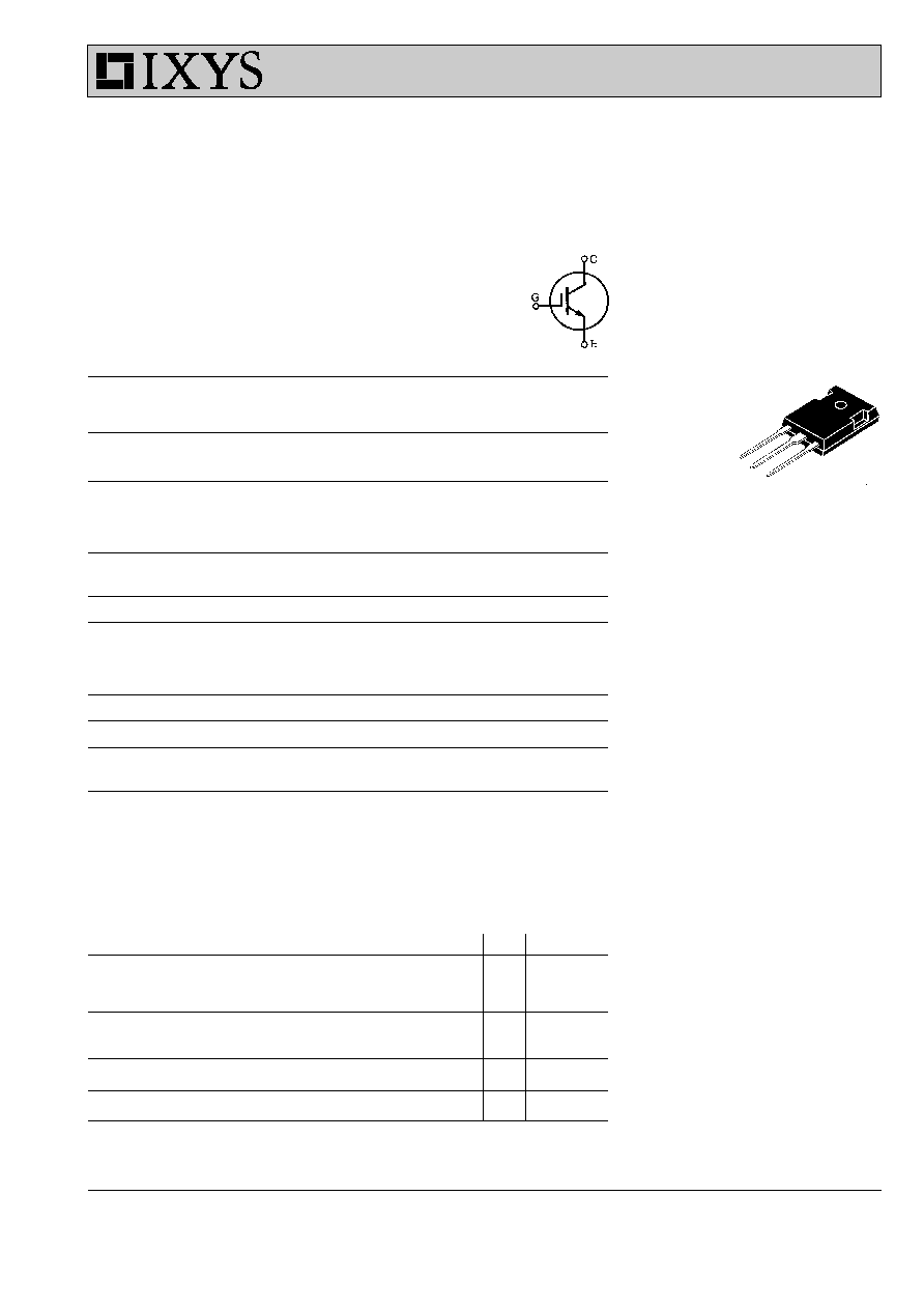
TO-247 AD
G
C
E
G = Gate,
C = Collector,
E = Emitter,
TAB = Collector
IXYS reserves the right to change limits, test conditions, and dimensions.
2 - 2
© 2000 IXYS All rights reserved
Symbol
Test Conditions
Characteristic Values
(T
J
= 25
∞
C, unless otherwise specified)
min.
typ.
max.
g
fs
I
C
= I
C90
; V
CE
= 10 V,
19
28
S
Pulse test, t
£
300
m
s, duty cycle
£
2 %
C
ies
2750
pF
C
oes
V
CE
= 25 V, V
GE
= 0 V, f = 1 MHz
206
pF
C
res
55
pF
Q
g
120
nC
Q
ge
I
C
= I
C90
, V
GE
= 15 V, V
CE
= 0.5 V
CES
25
nC
Q
gc
40
nC
t
d(on)
30
ns
t
ri
30
ns
t
d(off)
600
ns
t
fi
450
ns
E
off
8
mJ
t
d(on)
40
ns
t
ri
40
ns
E
on
0.3
mJ
t
d(off)
800
ns
t
fi
600
ns
E
off
15
mJ
R
thJC
0.62 K/W
R
thCK
0.25
K/W
Inductive load, T
J
= 25
∞
C
I
C
= I
C90
, V
GE
= 15 V, L = 100
m
H,
V
CE
= 0.8 V
CES
, R
G
= R
off
= 10
W
Remarks: Switching times may increase
for V
CE
(Clamp) > 0.8 ∑ V
CES
, higher T
J
or
increased R
G
Inductive load, T
J
= 125
∞
C
I
C
= I
C90
, V
GE
= 15 V, L = 100
m
H
V
CE
= 0.8 V
CES
, R
G
= R
off
= 10
W
Remarks: Switching times may increase
for V
CE
(Clamp) > 0.8 ∑ V
CES
, higher T
J
or
increased R
G
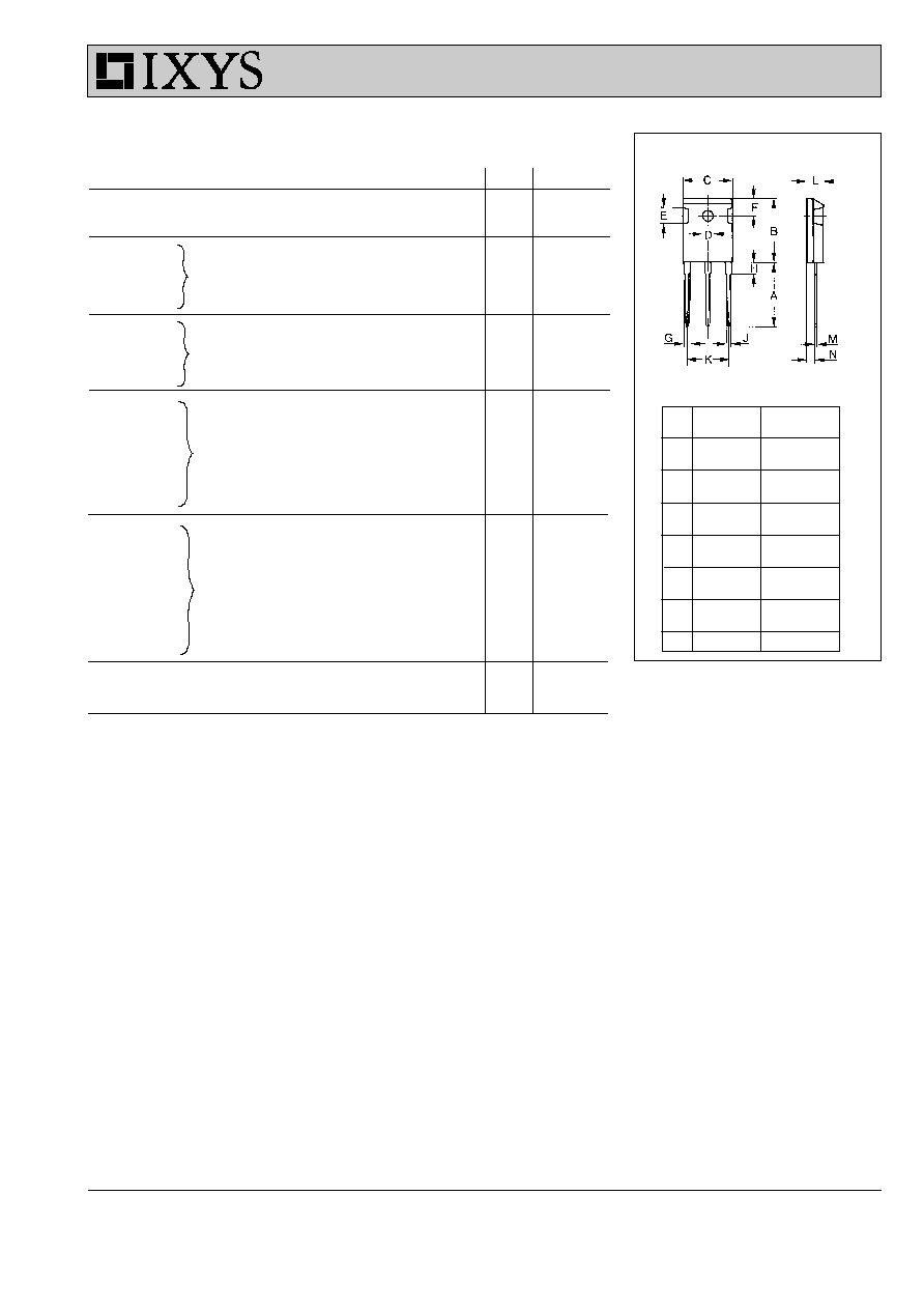
TO-247 AD (IXGH) Outline
Dim. Millimeter
Inches
Min.
Max.
Min.
Max.
A
19.81 20.32
0.780 0.800
B
20.80 21.46
0.819 0.845
C
15.75 16.26
0.610 0.640
D
3.55
3.65
0.140 0.144
E
4.32
5.49
0.170 0.216
F
5.4
6.2
0.212 0.244
G
1.65
2.13
0.065 0.084
H
-
4.5
-
0.177
J
1.0
1.4
0.040 0.055
K
10.8
11.0
0.426 0.433
L
4.7
5.3
0.185 0.209
M
0.4
0.8
0.016 0.031
N
1.5
2.49
0.087 0.102
IXGH 41N60
IXYS MOSFETS and IGBTs are covered by one or more of the following U.S. patents:
4,835,592
4,881,106
5,017,508
5,049,961
5,187,117
5,486,715
4,850,072
4,931,844
5,034,796
5,063,307
5,237,481
5,381,025