 | –≠–ª–µ–∫—Ç—Ä–æ–Ω–Ω—ã–π –∫–æ–º–ø–æ–Ω–µ–Ω—Ç: 50N50B | –°–∫–∞—á–∞—Ç—å:  PDF PDF  ZIP ZIP |
© 2002 IXYS All rights reserved
Symbol
Test Conditions
Maximum Ratings
V
CES
T
J
= 25
∞
C to 150
∞
C
600
V
V
CGR
T
J
= 25
∞
C to 150
∞
C; R
GE
= 1 M
600
V
V
GES
Continuous
±
20
V
V
GEM
Transient
±
30
V
I
C25
T
C
= 25
∞
C
75
A
I
C90
T
C
= 90
∞
C
50
A
I
CM
T
C
= 25
∞
C, 1 ms
200
A
SSOA
V
GE
= 15 V, T
VJ
= 125
∞
C, R
G
= 10
I
CM
= 100
A
(RBSOA)
Clamped inductive load
@ 0.8 V
CES
P
C
T
C
= 25
∞
C
300
W
T
J
-55 ... +150
∞
C
T
JM
150
∞
C
T
stg
-55 ... +150
∞
C
M
d
Mounting torque
TO-247AD
1.13/10 Nm/lb.in.
TO-264
0.9/6 Nm/lb.in.
Maximum lead temperature for soldering
300
∞
C
1.6 mm (0.062 in.) from case for 10 s
Weight
TO-247
6
g
TO-264
10
g
TO-268
4
g
95585F(12/02)
V
CES
= 600 V
I
C25
= 75 A
V
CE(sat)
= 2.3
V
t
fi(typ)
= 120 ns
IXGH 50N60B
IXGK 50N60B
IXGT 50N60B
IXGJ 50N60B
Symbol
Test Conditions
Characteristic Values
(T
J
= 25
∞
C, unless otherwise specified)
Min.
Typ. Max.
BV
CES
I
C
= 250
µ
A, V
GE
= 0 V
600
V
V
GE(th)
I
C
= 250
µ
A, V
CE
= V
GE
2.5
5.0
V
I
CES
V
CE
= 0.8 ∑ V
CES
T
J
= 25
∞
C
200
µ
A
V
GE
= 0 V
T
J
= 125
∞
C
1
mA
I
GES
V
CE
= 0 V, V
GE
=
±
20 V
±
100
nA
V
CE(sat)
I
C
= I
C90
, V
GE
= 15 V
2.3
V
Features
∑ International standard packages
∑ High frequency IGBT
∑ Latest generation HDMOS
TM
process
∑ High current handling capability
∑ MOS Gate turn-on
- drive simplicity
Applications
∑ AC motor speed control
∑ DC servo and robot drives
∑ DC choppers
∑ Uninterruptible power supplies (UPS)
∑ Switch-mode and resonant-mode
power supplies
Advantages
∑ Easy to mount with 1 screw
(insulated mounting screw hole)
∑ Switching speed for high frequency
applications
∑ High power density
HiPerFAST
TM
IGBT
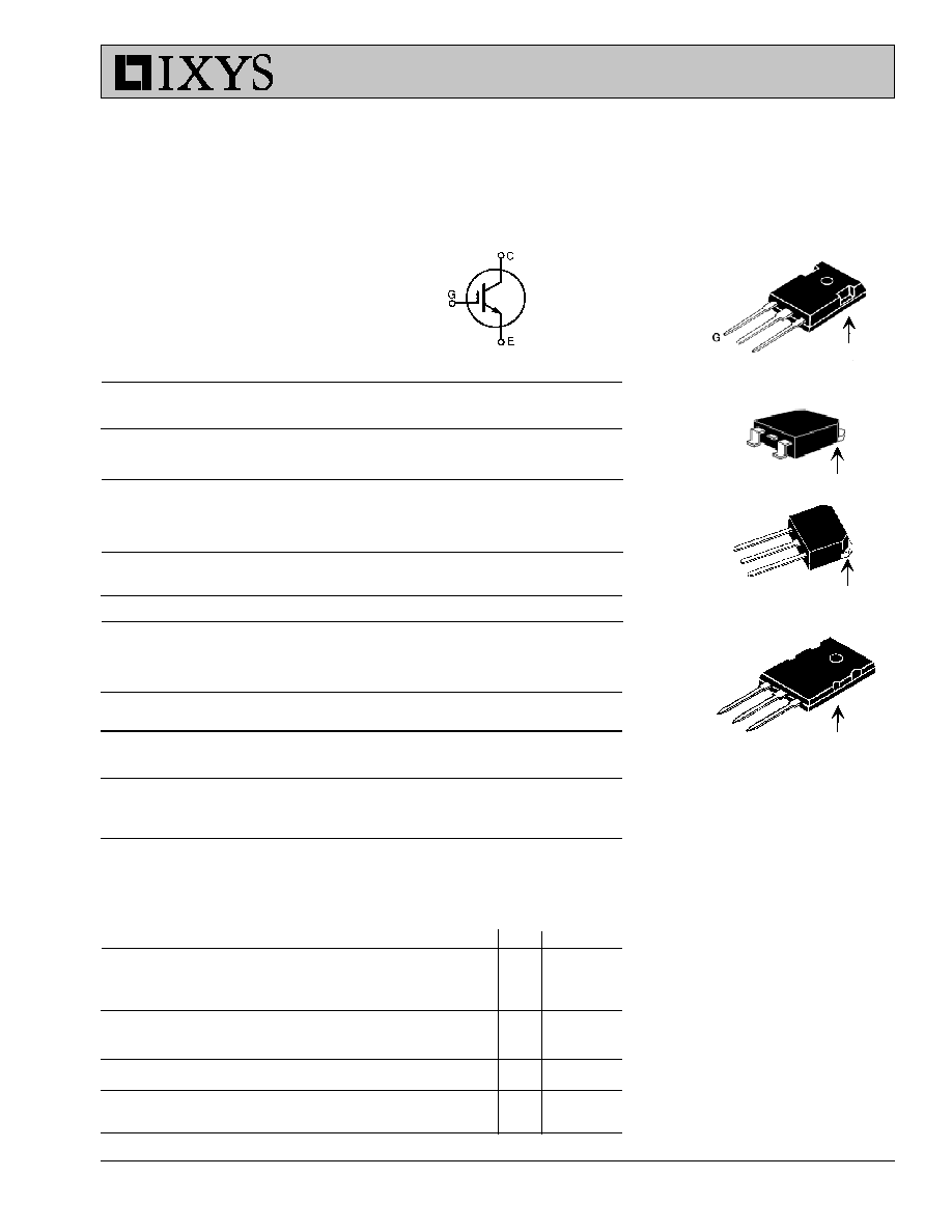
TO-247 AD (IXGH)
C
E
C (TAB)
TO-268 (D3) ( IXGT)
C (TAB)
G
E
G = Gate
D = Drain
E = Emitter
TAB = Collector
TO-264 AA (IXGK)
E
G
C
C (TAB)
(TAB)
G
C
E
TO-268 Leaded (IXGJ)

IXYS reserves the right to change limits, test conditions, and dimensions.
IXYS MOSFETS and IGBTs are covered by one or more of the following U.S. patents:
4,835,592
4,881,106
5,017,508
5,049,961
5,187,117
5,486,715
6,306,728B1
4,850,072
4,931,844
5,034,796
5,063,307
5,237,481
5,381,025
Symbol
Test Conditions
Characteristic Values
(T
J
= 25
∞
C, unless otherwise specified)
min. typ. max.
g
fs
I
C
= I
C90
; V
CE
= 10 V,
25
42
S
Pulse test, t
300
µ
s, duty cycle
2 %
C
ies
4100
pF
C
oes
V
CE
= 25 V, V
GE
= 0 V, f = 1 MHz
310
pF
C
res
95
pF
Q
G
160
nC
Q
GE
I
C
= I
C90
, V
GE
= 15 V, V
CE
= 0.5 V
CES
30
nC
Q
GC
55
nC
t
d(on)
50
ns
t
ri
50
ns
t
d(off)
150
250
ns
t
fi
120
250
ns
E
off
3.0
4.5
mJ
t
d(on)
50
ns
t
ri
50
ns
E
on
3
mJ
t
d(off)
200
ns
t
fi
250
ns
E
off
4.2
mJ
R
thJC
0.42 K/W
R
thCK
TO-247 & TO-268 leaded packages
0.25
K/W
TO-264 package
0.15
K/W
Dim.
Millimeter
Inches
Min.
Max.
Min.
Max.
A
4.7
5.3
.185
.209
A
1
2.2
2.54
.087
.102
A
2
2.2
2.6
.059
.098
b
1.0
1.4
.040
.055
b
1
1.65
2.13
.065
.084
b
2
2.87
3.12
.113
.123
C
.4
.8
.016
.031
D
20.80
21.46
.819
.845
E
15.75
16.26
.610
.640
e
5.20
5.72
0.205
0.225
L
19.81
20.32
.780
.800
L1
4.50
.177
P
3.55
3.65
.140
.144
Q
5.89
6.40
0.232
0.252
R
4.32
5.49
.170
.216
S
6.15 BSC
242 BSC
Terminals:
1 - Gate
2 -Collector
3 -Emitter
Tab-Collector
1 2 3
TO-247 AD (IXGH) Outline
IXGH 50N60B IXGK 50N60B
IXGJ 50N60B IXGT 50N60B
Inductive load, T
J
= 25
∞∞
∞∞
∞
C
I
C
= I
C90
, V
GE
= 15 V
V
CE
= 0.8 ∑ V
CES
, R
G
= R
off
= 2.7
Remarks: Switching times may increase
for V
CE
(Clamp) > 0.8 ∑ V
CES
, higher T
J
or
increased R
G
Inductive load, T
J
= 125
∞∞
∞∞
∞
C
I
C
= I
C90
, V
GE
= 15 V
V
CE
= 0.8 ∑ V
CES
, R
G
= R
off
= 2.7
Remarks: Switching times may increase
for V
CE
(Clamp) > 0.8 ∑ V
CES
, higher T
J
or
increased R
G
TO-264 AA (IXGK) Outline
Millimeter
Inches
Min.
Max.
Min.
Max.
A
4.82
5.13
.190
.202
A1
2.54
2.89
.100
.114
A2
2.00
2.10
.079
.083
b
1.12
1.42
.044
.056
b1
2.39
2.69
.094
.106
b2
2.90
3.09
.114
.122
c
0.53
0.83
.021
.033
D
25.91
26.16
1.020
1.030
E
19.81
19.96
.780
.786
e
5.46 BSC
.215 BSC
J
0.00
0.25
.000
.010
K
0.00
0.25
.000
.010
L
20.32
20.83
.800
.820
L1
2.29
2.59
.090
.102
P
3.17
3.66
.125
.144
Q
6.07
6.27
.239
.247
Q1
8.38
8.69
.330
.342
R
3.81
4.32
.150
.170
R1
1.78
2.29
.070
.090
S
6.04
6.30
.238
.248
T
1.57
1.83
.062
.072
Dim.
TO-268 (IXGJ) Leaded Outline
TO-268 (IXGT) Outline
Terminals:
1 - Gate
2 -
Collector

© 2002 IXYS All rights reserved
Figure 1. Saturation Voltage Characteristics
Figure 2. Extended Output Characteristics
Figure 3. Saturation Voltage Characteristics
Figure 4. Temperature Dependence of V
CE(sat)
Figure 5. Admittance Curves
Figure 6. Capacitance Curves
V
CE
- Volts
0
2
4
6
8
10
I
C
- A
m
p
e
r
e
s
0
40
80
120
160
200
V
GE
- Volts
0
2
4
6
8
10
I
C
-
A
m
p
e
r
e
s
0
20
40
60
80
100
V
CE
-Volts
0
5
10
15
20
25
30
35
40
Ca
paci
tanc
e -
pF
10
100
1000
10000
T
J
- Degrees C
25
50
75
100
125
150
V
C
E
(sat)
-
N
o
r
m
a
liz
ed
0.4
0.6
0.8
1.0
1.2
1.4
1.6
V
CE
- Volts
0
1
2
3
4
5
I
C
-
A
m
p
e
re
s
0
20
40
60
80
100
9V
5V
V
CE
= 10V
T
J
= 25∞C
T
J
= 25∞C
I
C
= 25A
I
C
= 50A
I
C
= 100A
T
J
=
125∞C
f = 1Mhz
7V
V
GE
= 15V
T
J
= 25∞C
V
CE
- Volts
0
1
2
3
4
5
I
C
- A
m
p
e
re
s
0
20
40
60
80
100
T
J
= 125∞C
C
iss
C
oss
7V
5V
V
GE
= 15V
13V
11V
9V
9V
V
GE
= 15V
13V
11V
V
GE
= 15V
13V
7V
11V
C
rss
5V
IXGH 50N60B IXGK 50N60B
IXGJ 50N60B IXGT 50N60B

IXYS reserves the right to change limits, test conditions, and dimensions.
IXYS MOSFETS and IGBTs are covered by one or more of the following U.S. patents:
4,835,592
4,881,106
5,017,508
5,049,961
5,187,117
5,486,715
6,306,728B1
4,850,072
4,931,844
5,034,796
5,063,307
5,237,481
5,381,025
IXGH 50N60B IXGK 50N60B
IXGJ 50N60B IXGT 50N60B
R
G
- Ohms
0
10
20
30
40
50
60
E
(O
F
F
)
- m
illi
jou
l
es
0
2
4
6
8
10
12
E
(O
N)
-
m
i
llijo
ule
s
0
1
2
3
4
5
6
Pulse Width - Seconds
0.00001
0.0001
0.001
0.01
0.1
1
Z
th
J
C
(K/W
)
0.001
0.01
0.1
1
D=0.02
V
CE
- Volts
0
100
200
300
400
500
600
I
C
-
Am
pe
re
s
0.1
1
10
100
Q
g
- nanocoulombs
0
40
80
120
160
200
V
GE
- Vo
lts
0
4
8
12
16
I
C
- Amperes
0
20
40
60
80
100
E
(
O
FF)
-
m
illiJ
ou
le
s
0
2
4
6
8
10
12
E
(O
N
)
- m
illij
oul
es
0
1
2
3
4
5
6
V
CE
= 250V
I
C
= 25A
E
(ON)
E
(OFF)
E
(ON)
E
(OFF)
T
J
= 125∞C
R
G
= 6.2
dV/dt < 5V/ns
D=0.1
D=0.05
Single pulse
D = Duty Cycle
T
J
= 125∞C
600
E
(OFF)
D=0.2
D=0.5
D=0.01
R
G
= 4.7
I
C
=25A
T
J
= 125∞C
I
C
= 100A
I
C
= 50A
E
(ON)
E
(ON)
E
(OFF)
Figure 7. Dependence of E
ON
and E
OFF
on I
C
Figure 8. Dependence of E
ON
and E
OFF
on R
G
Figure 9. Gate Charge
Figure 10. Turn-off Safe Operating Area
Figure 11. IGBT Transient Thermal Resistance