© 1996 IXYS All rights reserved
Features
l
International standard packages
JEDEC TO-247 SMD surface
mountable and JEDEC TO-247 AD
l
High frequency IGBT
l
High current handling capability
l
2nd generation HDMOS
TM
process
l
MOS Gate turn-on
- drive simplicity
Applications
l
AC motor speed control
l
DC servo and robot drives
l
DC choppers
l
Uninterruptible power supplies (UPS)
l
Switch-mode and resonant-mode
power supplies
Advantages
l
High power density
l
Suitable for surface mounting
l
Switching speed for high frequency
applications
l
Easy to mount with 1 screw, TO-247
(insulated mounting screw hole)
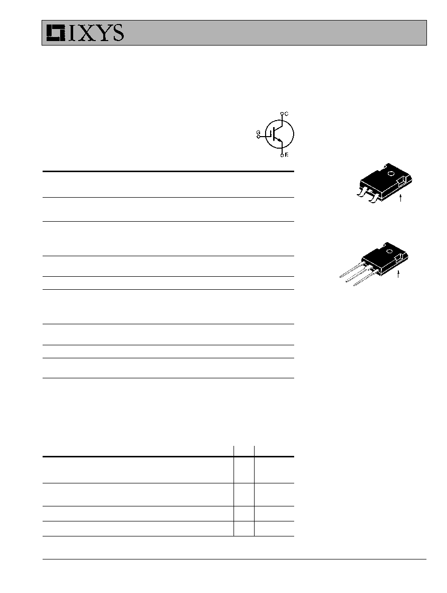
Symbol
Test Conditions
Characteristic Values
(T
J
= 25
∞
C, unless otherwise specified)
min.
typ.
max.
BV
CES
I
C
= 250
µ
A, V
GE
= 0 V
600
V
V
GE(th)
I
C
= 250
µ
A, V
CE
= V
GE
2.5
5
V
I
CES
V
CE
= 0.8 ∑ V
CES
T
J
= 25
∞
C
200
µ
A
V
GE
= 0 V
T
J
= 125
∞
C
1
mA
I
GES
V
CE
= 0 V, V
GE
=
±
20 V
±
100
nA
V
CE(sat)
I
C
= I
C90
, V
GE
= 15 V
2.7
V
TO-247 AD
(50N60A)
G
C
E
C (TAB)
G = Gate,
C = Collector,
E = Emitter,
TAB = Collector
92797H(9/96)
E
G
C (TAB)
V
CES
=
600 V
I
C25
=
75 A
V
CE(sat)
=
2.7 V
t
fi
= 275 ns
IXGH50N60A
IXGH50N60AS
HiPerFAST
TM
IGBT
Surface Mountable
Symbol
Test Conditions
Maximum Ratings
V
CES
T
J
= 25
∞
C to 150
∞
C
600
V
V
CGR
T
J
= 25
∞
C to 150
∞
C; R
GE
= 1 M
600
V
V
GES
Continuous
±
20
V
V
GEM
Transient
±
30
V
I
C25
T
C
= 25
∞
C
75
A
I
C90
T
C
= 90
∞
C
50
A
I
CM
T
C
= 25
∞
C, 1 ms
200
A
SSOA
V
GE
= 15 V, T
VJ
= 125
∞
C, R
G
= 10
I
CM
= 100
A
(RBSOA)
Clamped inductive load, L = 30
µ
H
@ 0.8 V
CES
P
C
T
C
= 25
∞
C
250
W
T
J
-55 ... +150
∞
C
T
JM
150
∞
C
T
stg
-55 ... +150
∞
C
Maximum Lead and Tab temperature for soldering
300
∞
C
1.6 mm (0.062 in.) from case for 10 s
M
d
Mounting torque, TO-247 AD
1.13/10 Nm/lb.in.
Weight
TO-247 SMD
4
g
TO-247 AD
6
g
TO-247 SMD
(50N60AS)
IXYS MOSFETS and IGBTs are covered by one or more of the following U.S. patents:
4,835,592
4,881,106
5,017,508
5,049,961
5,187,117
5,486,715
4,850,072
4,931,844
5,034,796
5,063,307
5,237,481
5,381,025
IXYS reserves the right to change limits, test conditions, and dimensions.
IXGH50N60A
IXGH50N60AS
Symbol
Test Conditions
Characteristic Values
(T
J
= 25
∞
C, unless otherwise specified)
min.
typ.
max.
g
fs
I
C
= I
C90
; V
CE
= 10 V,
25
35
S
Pulse test, t
300
µ
s, duty cycle
2 %
C
ies
4000
pF
C
oes
V
CE
= 25 V, V
GE
= 0 V, f = 1 MHz
430
pF
C
res
100
pF
Q
g
200
250
nC
Q
ge
I
C
= I
C90
, V
GE
= 15 V, V
CE
= 0.5 V
CES
35
50
nC
Q
gc
80
100
nC
t
d(on)
50
ns
t
ri
210
ns
t
d(off)
200
ns
t
fi
275
400
ns
E
off
4.8
mJ
t
d(on)
50
ns
t
ri
240
ns
E
on
3
mJ
t
d(off)
280
ns
t
fi
600
ns
E
off
9.6
mJ
R
thJC
0.50 K/W
R
thCK
0.25
K/W
Inductive load, T
J
= 25
∞∞
∞∞
∞
C
I
C
= I
C90
, V
GE
= 15 V, L = 30
µ
H,
V
CE
= 0.8 V
CES
, R
G
= R
off
= 2.7
Remarks: Switching times may increase
for V
CE
(Clamp) > 0.8 ∑ V
CES
, higher
T
J
or increased R
G
Inductive load, T
J
= 125
∞∞
∞∞
∞
C
I
C
= I
C90
, V
GE
= 15 V, L = 30
µ
H
V
CE
= 0.8 V
CES
, R
G
= R
off
= 2.7
Remarks: Switching times may increase
for V
CE
(Clamp) > 0.8 ∑ V
CES
,
higher T
J
or increased R
G
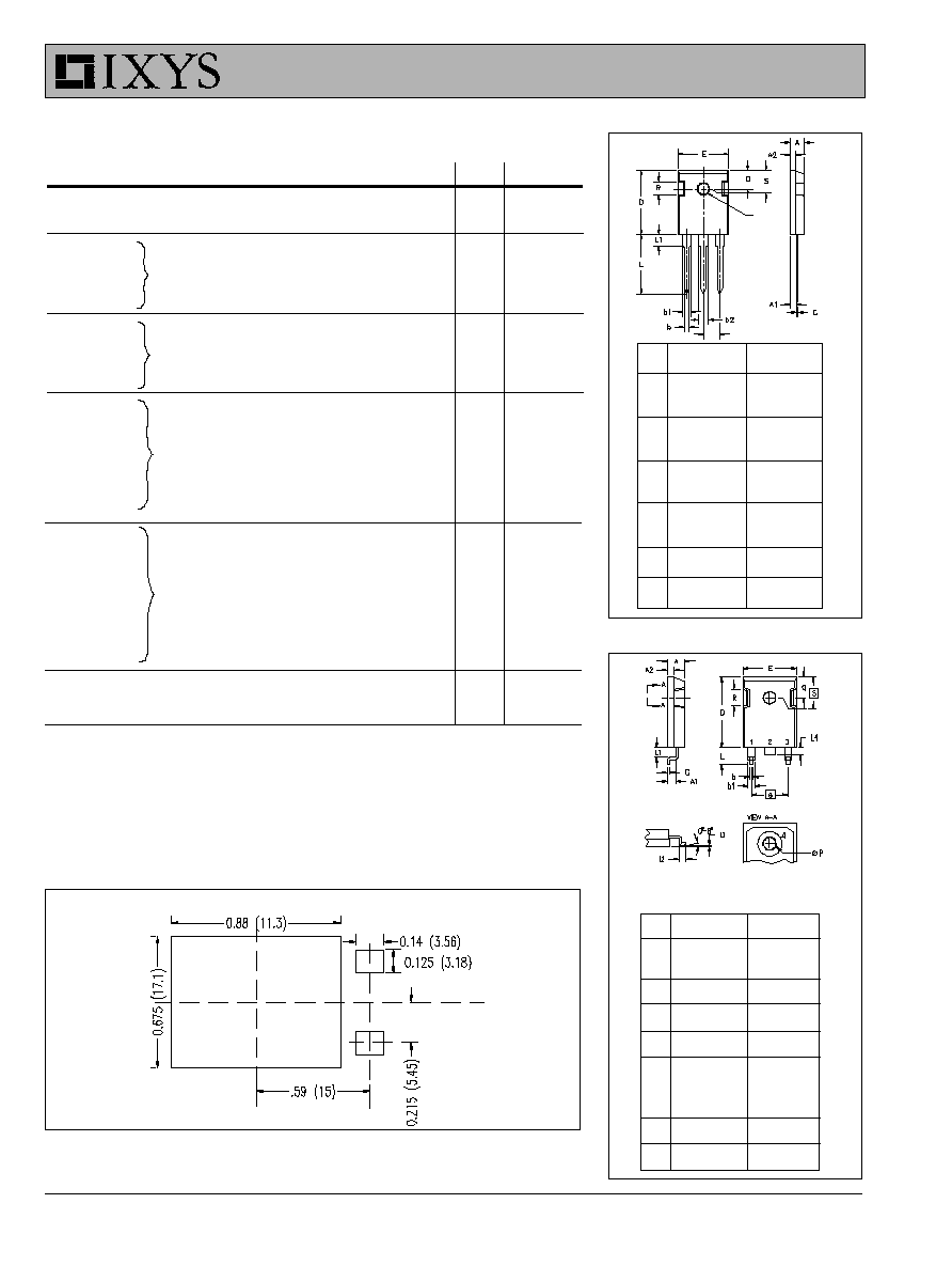
Min. Recommended Footprint (Dimensions in inches and (mm))
Dim.
Millimeter
Inches
Min.
Max.
Min.
Max.
A
4.7
5.3
.185
.209
A
1
2.2
2.54
.087
.102
A
2
2.2
2.6
.059
.098
b
1.0
1.4
.040
.055
b
1
1.65
2.13
.065
.084
b
2
2.87
3.12
.113
.123
C
.4
.8
.016
.031
D
20.80
21.46
.819
.845
E
15.75
16.26
.610
.640
e
5.20
5.72
0.205 0.225
L
19.81
20.32
.780
.800
L1
4.50
.177
P
3.55
3.65
.140
.144
Q
5.89
6.40
0.232 0.252
R
4.32
5.49
.170
.216
S
6.15 BSC
242 BSC
e
P
1. Gate
2. Collector
3. Emitter
4. Collector
Dim.
Millimeter
Inches
Min.
Max.
Min.
Max.
A
4.83
5.21
.190
.205
A1
2.29
2.54
.090
.100
A2
1.91
2.16
.075
.085
b
1.14
1.40
.045
.055
b1
1.91
2.13
.075
.084
C
0.61
0.80
.024
.031
D
20.80
21.34
.819
.840
E
15.75
16.13
.620
.635
e
5.45
BSC
.215
BSC
L
4.90
5.10
.193
.201
L1
2.70
2.90
.106
.114
L2
2.10
2.30
.083
.091
L3
0.00
0.10
.00
.004
L4
1.90
2.10
.075
.083
ÿP
3.55
3.65
.140
.144
Q
5.59
6.20
.220
.244
R
4.32
4.83
.170
.190
S
6.15
BSC
.242
BSC
TO-247 SMD Outline
TO-247 AD Outline
© 1996 IXYS All rights reserved
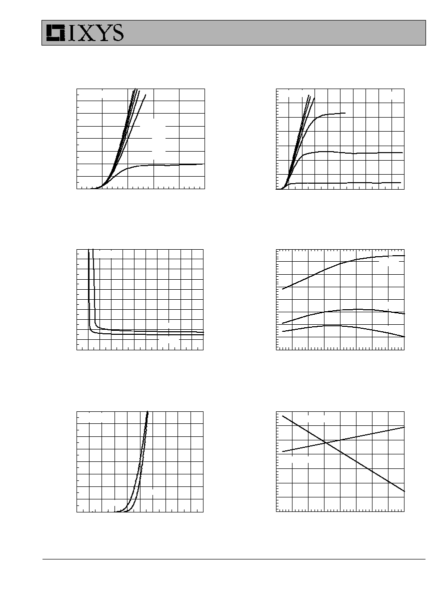
T
J
- Degrees C
-50
-25
0
25
50
75
100 125 150
BV
/ V
C
E
(sa
t
)
-
No
rm
aliz
ed
0.5
0.6
0.7
0.8
0.9
1.0
1.1
1.2
V
GE
- Volts
0
1
2
3
4
5
6
7
8
9
10
I
C
-
Am
pe
res
0
10
20
30
40
50
60
70
80
T
J
- Degrees C
-50
-25
0
25
50
75
100 125 150
V
C
E
(sa
t
)
-
No
rma
lize
d
0.7
0.8
0.9
1.0
1.1
1.2
1.3
1.4
1.5
V
GE
- Volts
4
5
6
7
8
9
10 11 12 13 14 15
V
CE
-
Vol
ts
0
1
2
3
4
5
6
7
8
9
10
V
CE
- Volts
0
2
4
6
8
10
12
14
16
18
20
I
C
-
Am
pe
res
0
50
100
150
200
250
300
350
5V
7V
9V
11V
13V
V
CE
- Volts
0
1
2
3
4
5
I
C
-
Am
pe
res
0
10
20
30
40
50
60
70
80
V
GE
= 15V
I
C
= 40A
I
C
= 20A
I
C
= 80A
I
C
= 40A
I
C
= 20A
T
J
=
125∞C
T
J
= 25∞C
V
GE(th)
@ 250µA
V
CE
= 100V
BV
CES
@ 3mA
T
J
= 25∞C
T
J
= 25∞C
T
J
= 25∞C
V
GE
= 15V
13V
11V
9V
7V
5V
Fig. 3 Collector-Emitter Voltage
Fig. 4
Temperature Dependence
vs. Gate-Emitter Voltage
of Output Saturation Voltage
Fig. 1 Saturation Characteristics
Fig. 2
Output Characterstics
Fig. 5 Input Admittance
Fig. 6
Temperature Dependence of
Breakdown and Threshold Voltage
IXGH50N60A
IXGH50N60AS
IXYS MOSFETS and IGBTs are covered by one or more of the following U.S. patents:
4,835,592
4,881,106
5,017,508
5,049,961
5,187,117
5,486,715
4,850,072
4,931,844
5,034,796
5,063,307
5,237,481
5,381,025
IXYS reserves the right to change limits, test conditions, and dimensions.
IXGH50N60A
IXGH50N60AS
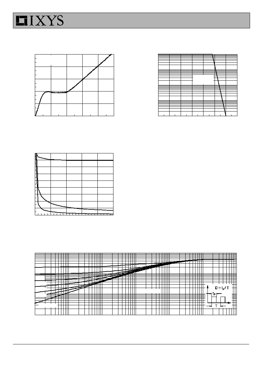
V
CE
- Volts
0
5
10
15
20
25
C
a
p
aci
tan
ce
- pF
0
500
1000
1500
2000
2500
3000
3500
4000
4500
C
ies
C
res
C
oes
V
CE
- Volts
0
100
200
300
400
500
600
700
I
C
-
Am
pe
res
0.01
0.1
1
10
100
T
J
= 125∞C
dV/dt < 3V/ns
Total Gate Charge - (nC)
0
50
100
150
200
250
V
GE
-
Vo
lts
0
3
6
9
12
15
Pulse Width - seconds
0.00001
0.0001
0.001
0.01
0.1
1
10
Z
th
J
C
(
K/W
)
0.001
0.01
0.1
1
D = Duty Cycle
Single Pulse
D=0.5
D=0.2
I
C
= 40A
V
CE
= 500V
D=0.1
D=0.05
D=0.02
D=0.01
G50N60 2 JNB
Fig.10 Transient Thermal Impedance
Fig.9 Capacitance Curves
Fig.7 Gate Charge
Fig.8 Turn-Off Safe Operating Area