 | –≠–ª–µ–∫—Ç—Ä–æ–Ω–Ω—ã–π –∫–æ–º–ø–æ–Ω–µ–Ω—Ç: 52N60AU1 | –°–∫–∞—á–∞—Ç—å:  PDF PDF  ZIP ZIP |
1 - 5
© 2000 IXYS All rights reserved
Symbol
Test Conditions
Maximum Ratings
V
CES
T
J
= 25
∞
C to 150
∞
C
600
V
V
CGR
T
J
= 25
∞
C to 150
∞
C; R
GE
= 1 M
W
600
A
V
GES
Continuous
±
20
V
V
GEM
Transient
±
30
V
I
C25
T
C
= 25
∞
C
80
A
I
C90
T
C
= 90
∞
C
40
A
I
CM
T
C
= 25
∞
C, 1 ms
160
A
SSOA
V
GE
= 15 V, T
VJ
= 125
∞
C, R
G
= 22
W
I
CM
= 80
A
(RBSOA)
Clamped inductive load, L = 30
m
H
@ 0.8 V
CES
t
SC
V
GE
= 15 V, V
CE
= 360 V, T
J
= 125
∞
C
10
m
s
(SCSOA)
R
G
= 22
W
, non repetitive
P
C
T
C
= 25
∞
C
250
W
V
ISOL
50/60 Hz
t = 1 min
2500
V~
I
ISOL
£
1 mA
t = 1 s
3000
V~
T
J
-55 ... +150
∞
C
T
JM
150
∞
C
T
stg
-55 ... +150
∞
C
M
d
Mounting torque
1.5/13
Nm/lb.in.
Terminal connection torque (M4)
1.5/13
Nm/lb.in.
Weight
30
g
IGBT with Diode
IXSN 52N60AU1
V
CES
= 600 V
I
C25
= 80 A
Combi Pack
V
CE(sat)
= 3 V
Short Circuit SOA Capability
Symbol
Test Conditions
Characteristic Values
(T
J
= 25
∞
C, unless otherwise specified)
min.
typ.
max.
BV
CES
I
C
= 3 mA, V
GE
= 0 V
600
V
V
GE(th)
I
C
= 4 mA, V
CE
= V
GE
4
8
V
I
CES
V
CE
= 0.8 ∑ V
CES
T
J
= 25
∞
C
750
m
A
V
GE
= 0 V
T
J
= 125
∞
C
15
mA
I
GES
V
CE
= 0 V, V
GE
=
±
20 V
±
100
nA
V
CE(sat)
I
C
= I
C90
, V
GE
= 15 V
3
V
miniBLOC, SOT-227 B
2
1
4
3
2
4
Features
∑ International standard package
miniBLOC
∑ Aluminium-nitride isolation
- high power dissipation
∑ Isolation voltage 3000 V~
∑ Low V
CE(sat)
- for minimum on-state conduction
losses
∑ Fast Recovery
Epitaxial Diode
- short t
rr
and I
RM
∑ Low collector-to-case capacitance
(< 50 pF)
- reducesd RFI
∑ Low package inductance (< 10 nH)
- easy to drive and to protect
Applications
∑ AC motor speed control
∑ DC servo and robot drives
∑ DC choppers
∑ Uninterruptible power supplies (UPS)
∑ Switch-mode and resonant-mode
power supplies
Advantages
∑ Space savings
∑ Easy to mount with 2 screws
∑ High power density
3
1
1 = Emitter
,
3 = Collector
2 = Gate,
4 = Emitter
Either Emitter terminal can be used as
Main or Kelvin Emitter
92814H(5/97)
IXYS reserves the right to change limits, test conditions, and dimensions.

2 - 5
© 2000 IXYS All rights reserved
Symbol
Test Conditions
Characteristic Values
(T
J
= 25
∞
C, unless otherwise specified)
min.
typ.
max.
g
fs
I
C
= I
C90
; V
CE
= 10 V,
20
23
S
Pulse test, t
£
300
m
s, duty cycle d
£
2 %
C
ies
4500
pF
C
oes
V
CE
= 25 V, V
GE
= 0 V, f = 1 MHz
400
pF
C
res
90
pF
Q
g
190
250
nC
Q
ge
I
C
= I
C90
, V
GE
= 15 V, V
CE
= 0.5 V
CES
45
60
nC
Q
gc
88
120
nC
t
d(on)
70
ns
t
ri
220
ns
t
d(off)
200
ns
t
fi
200
ns
E
off
3.5
mJ
t
d(on)
70
ns
t
ri
220
ns
E
on
4.7
mJ
t
d(off)
450
ns
t
fi
340
600
ns
E
off
6
mJ
R
thJC
0.50 K/W
R
thCK
0.05
K/W
Reverse Diode (FRED)
Characteristic Values
(T
J
= 25
∞
C, unless otherwise specified)
Symbol
Test Conditions
min.
typ.
max.
V
F
I
F
= I
C90
, V
GE
= 0 V,
1.8
V
Pulse test, t
£
300
m
s, duty cycle d
£
2 %
I
RM
I
F
= I
C90
, V
GE
= 0 V, -di
F
/dt = 480 A/
m
s
19
A
t
rr
V
R
= 360 V
T
J
= 125
∞
C
175
ns
I
F
= 1 A; -di/dt = 200 A/
m
s; V
R
= 30 V
T
J
= 25
∞
C
35
50
ns
R
thJC
0.80 K/W
Inductive load, T
J
= 25
∞
C
I
C
= I
C90
, V
GE
= 15 V, L = 100
m
H,
V
CE
= 0.8 V
CES
, R
G
= 2.7
W
Remarks: Switching times may increase
for V
CE
(Clamp) > 0.8 ∑ V
CES
, higher T
J
or
increased R
G
Inductive load, T
J
= 125
∞
C
I
C
= I
C90
, V
GE
= 15 V, L = 100
m
H
V
CE
= 0.8 V
CES
, R
G
= 2.7
W
Remarks: Switching times may increase
for V
CE
(Clamp) > 0.8 ∑ V
CES
, higher T
J
or
increased R
G
M4 screws (4x) supplied
Dim.
Millimeter
Inches
Min.
Max.
Min.
Max.
A
31.50
31.88
1.240
1.255
B
7.80
8.20
0.307
0.323
C
4.09
4.29
0.161
0.169
D
4.09
4.29
0.161
0.169
E
4.09
4.29
0.161
0.169
F
14.91
15.11
0.587
0.595
G
30.12
30.30
1.186
1.193
H
38.00
38.23
1.496
1.505
J
11.68
12.22
0.460
0.481
K
8.92
9.60
0.351
0.378
L
0.76
0.84
0.030
0.033
M
12.60
12.85
0.496
0.506
N
25.15
25.42
0.990
1.001
O
1.98
2.13
0.078
0.084
P
4.95
5.97
0.195
0.235
Q
26.54
26.90
1.045
1.059
R
3.94
4.42
0.155
0.174
S
4.72
4.85
0.186
0.191
T
24.59
25.07
0.968
0.987
U
-0.05
0.1
-0.002
0.004
miniBLOC, SOT-227 B
IXSN52N60AU1
IXYS MOSFETS and IGBTs are covered by one or more of the following U.S. patents:
4,835,592
4,881,106
5,017,508
5,049,961
5,187,117
5,486,715
4,850,072
4,931,844
5,034,796
5,063,307
5,237,481
5,381,025

3 - 5
© 2000 IXYS All rights reserved
IXSN52N60AU1
T
J
- Degrees C
-50
-25
0
25
50
75
100 125 150
BV
/
V
GE
(
t
h)
-
No
rma
l
iz
e
d
0.7
0.8
0.9
1.0
1.1
1.2
1.3
BV
CES
I
C
= 3mA
V
GE
- Volts
4
5
6
7
8
9
10
11
12
13
I
C
-
Am
per
es
0
10
20
30
40
50
60
70
80
T
J
- Degrees C
-50
-25
0
25
50
75
100 125 150
V
CE
(
s
a
t
)
- No
r
m
a
liz
e
d
0.7
0.8
0.9
1.0
1.1
1.2
1.3
1.4
1.5
V
GE
- Volts
8
9
10
11
12
13
14
15
V
CE
- V
o
lts
0
1
2
3
4
5
6
7
8
9
10
V
CE
- Volts
0
2
4
6
8
10
12 14 16 18 20
I
C
-
Am
per
es
0
20
40
60
80
100
120
140
160
180
200
7V
9V
11V
13V
V
CE
- Volts
0
1
2
3
4
5
I
C
-
Am
per
es
0
10
20
30
40
50
60
70
80
11V
7V
9V
13V
T
J
= 25∞C
V
GE
= 15V
T
J
= 25∞C
V
GE
= 15V
T
J
= 25∞C
I
C
= 20A
I
C
= 40A
I
C
= 80A
I
C
= 20A
I
C
= 40A
I
C
= 80A
V
GE
=15V
V
CE
= 10V
T
J
= 125∞C
T
J
= 25∞C
T
J
= - 40∞C
V
GE8th)
I
C
= 4mA
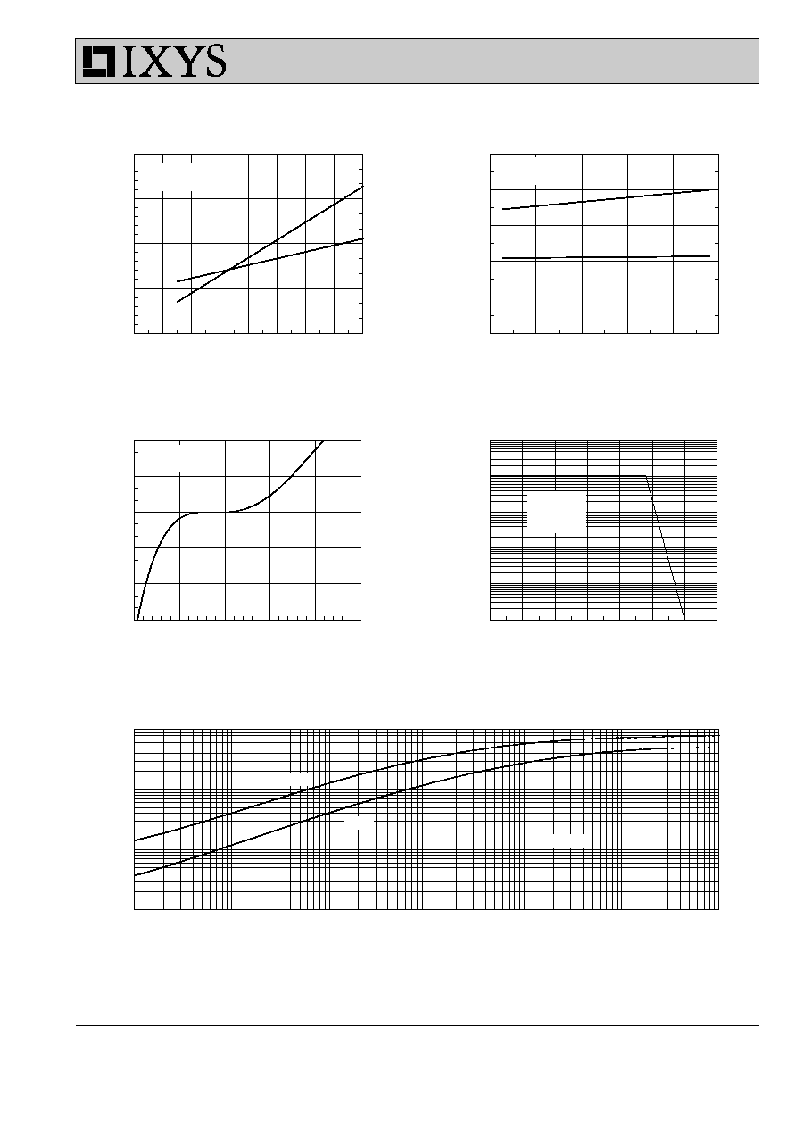
Fig.3 Collector-Emitter Voltage
Fig.4 Temperature Dependence
vs. Gate-Emitter Voltage
of Output Saturation Voltage
Fig.5 Input Admittance
Fig.6 Temperature Dependence of
Breakdown and Threshold Voltage
Fig.1 Saturation Characteristics
Fig.2 Output Characterstics
4 - 5
© 2000 IXYS All rights reserved
IXSN52N60AU1
R
G
- Ohms
0
10
20
30
40
50
E
of
f
-
m
illijo
u
l
e
s
0
2
4
6
8
10
t
fi
-
nan
os
e
c
o
nds
0
200
400
600
800
1000
V
CE
- Volts
0
100
200
300
400
500
600
700
I
C
- A
m
p
e
re
s
0.01
0.1
1
10
100
1000
T
J
= 125∞C
R
G
= 2.7
W
dV/dt < 6V/ns
Q
g
- nCoulombs
0
50
100
150
200
250
V
GE
- V
o
l
t
s
0
3
6
9
12
15
t
fi
E
off
I
C
- Amperes
0
10
20
30
40
50
60
70
80
t
fi
-
nanosecond
s
0
250
500
750
1000
E
of
f
-
m
i
llijo
u
l
e
s
0
3
6
9
12
t
fi
E
off
Time - Seconds
0.00001
0.0001
0.001
0.01
0.1
1
10
Ther
m
a
l
R
e
spon
s
e
-
K/
W
0.001
0.01
0.1
1
T
J
= 125∞C
R
G
= 10
W
IGBT
T
J
= 125∞C
I
C
= 52A
I
C
= 52A
V
CE
= 480V
Diode
Single Pulse
Fig.11 Transient Thermal Impedance
Fig.9 Gate Charge Characteristic Curve
Fig.10 Turn-Off Safe Operating Area
Fig.7 Turn-Off Energy per Pulse and
Fig.8 Dependence of Turn-Off Energy
Fall Time on Collector Current
Per Pulse and Fall Time on R
G

5 - 5
© 2000 IXYS All rights reserved
IXSN52N60AU1
Fig. 12 Forward current
Fig. 13 Recovery charge versus -di
F
/dt.
Fig. 14 Peak reverse current versus
versus voltage drop.
-di
F
/dt.
Fig. 15. Dynamic parameters versus
Fig. 16 Recovery time versus -di
F
/dt.
Fig. 17 Peak forward voltage vs. di
F
/dt.
junction temperature.
Fig. 18 Transient thermal impedance junction to case.