
© 2001 IXYS All rights reserved
Symbol
Test Conditions
Maximum Ratings
IXFK
IXFN
V
DSS
T
J
= 25∞C to 150∞C
300
300
V
V
DGR
T
J
= 25∞C to 150∞C; R
GS
= 1 M
300
300
V
V
GS
Continuous
±20
±20
V
V
GSM
Transient
±30
±30
V
I
D25
T
C
= 25∞C
73
73
A
I
DM
T
C
= 25∞C, pulse width limited by T
JM
292
292
A
I
AR
T
C
= 25∞C
40
40
A
E
AR
T
C
= 25∞C
30
30
mJ
dv/dt
I
S
I
DM
, di/dt
100 A/
µ
s, V
DD
V
DSS
,
5
5
V/ns
T
J
150∞C, R
G
= 2 W
P
D
T
C
= 25∞C
500
520
W
T
J
-55 ... +150
∞ C
T
JM
150
∞ C
T
stg
-55 ... +150
∞ C
T
L
1.6 mm (0.063 in) from case for 10 s
300
-
∞ C
V
ISOL
50/60 Hz, RMS
t = 1 min
-
2500
V~
I
ISOL
1 mA
t = 1 s
-
3000
V~
M
d
Mounting torque
0.9/6
1.5/13 Nm/lb.in.
Terminal connection torque
-
1.5/13 Nm/lb.in.
Weight
10
30
g
HiPerFET
TM
Power MOSFETs
N-Channel Enhancement Mode
Avalanche Rated, High dv/dt, Low t
rr
Features
l
International standard packages
l
JEDEC
TO-264 AA,
epoxy
meet
UL
94
V-0, flammability classification
l
miniBLOC with Aluminium nitride
isolation
l
Low R
DS (on)
HDMOS
TM
process
l
Rugged polysilicon gate cell structure
l
Unclamped Inductive Switching (UIS)
rated
l
Low package inductance
l
Fast intrinsic Rectifier
Applications
l
DC-DC converters
l
Synchronous rectification
l
Battery chargers
l
Switched-mode and resonant-mode
power supplies
l
DC choppers
l
Temperature and lighting controls
l
Low voltage relays
Advantages
l
Easy to mount
l
Space savings
l
High power density
Symbol
Test Conditions
Characteristic Values
(T
J
= 25∞C, unless otherwise specified)
min.
typ.
max.
V
DSS
V
GS
= 0 V, I
D
= 1 mA
300
V
V
GS(th)
V
DS
= V
GS
, I
D
= 8 mA
2
4
V
I
GSS
V
GS
= ±20 V
DC
, V
DS
= 0
±200
nA
I
DSS
V
DS
= 0.8 V
DSS
T
J
= 25∞C
400
uA
V
GS
= 0 V
T
J
= 125∞C
2
mA
R
DS(on)
V
GS
= 10 V, I
D
= 0.5 I
D25
45
m
Pulse test, t
300
µ
s, duty cycle d
2 %
TO-264 AA (IXFK)
TO-264 AA (IXFK)
TO-264 AA (IXFK)
TO-264 AA (IXFK)
TO-264 AA (IXFK)
S
G
D
G = Gate
D = Drain
S = Source
TAB = Drain
Either Source terminal at miniBLOC can be used
as Main or Kelvin Source
S
G
S
D
92805J (11/01)
miniBLOC, SOT-227 B (IXFN)
miniBLOC, SOT-227 B (IXFN)
miniBLOC, SOT-227 B (IXFN)
miniBLOC, SOT-227 B (IXFN)
miniBLOC, SOT-227 B (IXFN)
E153432
E153432
E153432
E153432
E153432
(TAB)
V
DSS
I
D25
R
DS(on)
IXFK 73 N 30
300 V
73 A
45 m
IXFN 73 N 30
300 V
73 A
45 m
t
rr
200 ns

IXYS MOSFETS and IGBTs are covered by one or more of the following U.S. patents:
4,835,592
4,881,106
5,017,508
5,049,961
5,187,117
5,486,715
4,850,072
4,931,844
5,034,796
5,063,307
5,237,481
5,381,025
IXYS reserves the right to change limits, test conditions, and dimensions.
IXFK 73N30
IXFN 73N30
TO-264 AA Outline
Millimeter
Inches
Min.
Max.
Min.
Max.
A
4.82
5.13
.190
.202
A1
2.54
2.89
.100
.114
A2
2.00
2.10
.079
.083
b
1.12
1.42
.044
.056
b1
2.39
2.69
.094
.106
b2
2.90
3.09
.114
.122
c
0.53
0.83
.021
.033
D
25.91
26.16
1.020
1.030
E
19.81
19.96
.780
.786
e
5.46 BSC
.215 BSC
J
0.00
0.25
.000
.010
K
0.00
0.25
.000
.010
L
20.32
20.83
.800
.820
L1
2.29
2.59
.090
.102
P
3.17
3.66
.125
.144
Q
6.07
6.27
.239
.247
Q1
8.38
8.69
.330
.342
R
3.81
4.32
.150
.170
R1
1.78
2.29
.070
.090
S6.04
6.30
.238
.248
T
1.57
1.83
.062
.072
Dim.
miniBLOC, SOT-227 B
M4 screws (4x) supplied
Dim.
Millimeter
Inches
Min.
Max.
Min.
Max.
A
31.50
31.88
1.240
1.255
B
7.80
8.20
0.307
0.323
C
4.09
4.29
0.161
0.169
D
4.09
4.29
0.161
0.169
E
4.09
4.29
0.161
0.169
F
14.91
15.11
0.587
0.595
G
30.12
30.30
1.186
1.193
H
38.00
38.23
1.496
1.505
J
11.68
12.22
0.460
0.481
K
8.92
9.60
0.351
0.378
L
0.76
0.84
0.030
0.033
M
12.60
12.85
0.496
0.506
N
25.15
25.42
0.990
1.001
O
1.98
2.13
0.078
0.084
P
4.95
5.97
0.195
0.235
Q
26.54
26.90
1.045
1.059
R
3.94
4.42
0.155
0.174
S4.72
4.85
0.186
0.191
T
24.59
25.07
0.968
0.987
U
-0.05
0.1
-0.002
0.004
Symbol
Test Conditions
Characteristic Values
(T
J
= 25∞C, unless otherwise specified)
min.
typ.
max.
g
fs
V
DS
= 10 V; I
D
= 0.5 I
D25
, pulse test
50
S
C
iss
9000
pF
C
oss
V
GS
= 0 V, V
DS
= 25 V, f = 1 MHz
1500
pF
C
rss
580
pF
t
d(on)
30
ns
t
r
V
GS
= 10 V, V
DS
= 0.5 V
DSS
, I
D
= 0.5 I
D25
80
ns
t
d(off)
R
G
= 1
(External),
100
ns
t
f
50
ns
Q
g(on)
360
nC
Q
gs
V
GS
= 10 V, V
DS
= 0.5 V
DSS
, I
D
= 0.5 I
D25
60
nC
Q
gd
180
nC
R
thJC
TO-264 AA
0.25
K/W
R
thCK
TO-264 AA
0.15
K/W
R
thJC
miniBLOC, SOT-227 B
0.24
K/W
R
thCK
miniBLOC, SOT-227 B
0.05
K/W
Source-Drain Diode
Characteristic Values
(T
J
= 25∞C, unless otherwise specified)
Symbol
Test Conditions
min.
typ.
max.
I
S
V
GS
= 0 V
73
A
I
SM
Repetitive; pulse width limited by T
JM
292
A
V
SD
I
F
= 100 A, V
GS
= 0 V,
1.5
V
Pulse test, t
300
µ
s, duty cycle d
2 %
t
rr
200
ns
Q
RM
I
F
= I
S
, -di/dt = 100 A/
µ
s, V
R
= 100 V
2
µ
C
I
RM
40
A
© 2001 IXYS All rights reserved
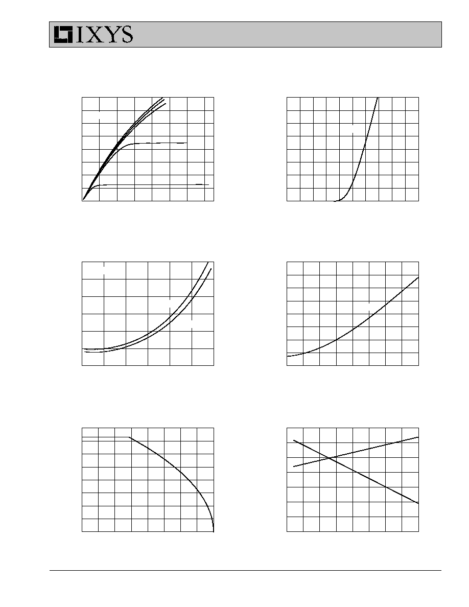
Fig. 1 Output Characteristics
Fig. 2 Input Admittance
Fig. 5 Drain Current vs.
Fig. 6 Temperature Dependence of
Case Temperature
Breakdown and Threshold Voltage
Fig. 3 R
DS(on)
vs. Drain Current
Fig. 4 Temperature Dependence
of Drain to Source Resistance
5V
T
J
- Degrees C
-50 -25
0
25
50
75
100 125 150
BV/
V
G(
t
h
)
- N
o
rm
a
l
iz
e
d
0.5
0.6
0.7
0.8
0.9
1.0
1.1
1.2
T
C
- Degrees C
-50 -25
0
25
50
75
100 125 150
I
D
-
A
m
per
es
0
10
20
30
40
50
60
70
80
T
J
- Degrees C
-50 -25
0
25
50
75
100 125 150
R
DS
(
on)
- No
rm
a
l
iz
e
d
0.50
0.75
1.00
1.25
1.50
1.75
2.00
2.25
2.50
I
D
- Amperes
0
40
80
120
160
200
240
R
DS
(
on)
- No
rm
a
l
iz
e
d
0.8
1.0
1.2
1.4
1.6
1.8
2.0
V
GS
- Volts
0
1
2
3
4
5
6
7
8
9
10
I
D
-
Am
per
es
0
20
40
60
80
100
120
140
160
8V
7V
6V
I
D
= 40A
V
GS(th)
BV
DSS
V
GS
= 10V
V
GS
= 10V
V
GS
= 15V
V
DS
- Volts
0
2
4
6
8
10
12
14
I
D
-
Am
per
es
0
20
40
60
80
100
120
140
160
T
J
= 25∞C
T
J
= 25∞C
T
J
= 25∞C
IXFK 73N30
IXFK 73N30
IXFK 73N30
IXFK 73N30
IXFK 73N30
IXFN 73N30
IXFN 73N30
IXFN 73N30
IXFN 73N30
IXFN 73N30

IXYS MOSFETS and IGBTs are covered by one or more of the following U.S. patents:
4,835,592
4,881,106
5,017,508
5,049,961
5,187,117
5,486,715
4,850,072
4,931,844
5,034,796
5,063,307
5,237,481
5,381,025
IXYS reserves the right to change limits, test conditions, and dimensions.
IXFK 73N30
IXFN 73N30
Fig.10 Transient Thermal Impedance
Time - Seconds
0.001
0.01
0.1
1
T
her
mal
Re
sp
ons
e -
K/
W
0.01
0.1
V
DS
- Volts
0
5
10
15
20
25
Ca
pa
c
i
t
a
nc
e
- p
F
0
1000
2000
3000
4000
5000
6000
7000
8000
9000
10000
C
rss
V
SD
- Volts
0.0
0.2
0.4
0.6
0.8
1.0
1.2
1.4
1.6
I
D
-
A
m
p
e
r
e
s
0
20
40
60
80
100
120
140
160
Gate Charge - nCoulombs
0
50
100 150 200 250 300 350 400
V
GE
-
V
o
lt
s
0
2
4
6
8
10
C
oss
V
DS
= 150V
I
D
= 42A
I
G
= 10mA
T
J
= 125∞C
C
iss
f = 1MHz
V
DS
= 25V
T
J
= 25∞C
Fig.7 Gate Charge Characteristic Curve
Fig.8 Capacitance Curves
Fig.9 Source Current vs. Source
to Drain Voltage