DE375-102N10A
RF Power MOSFET
V
DSS
= 1000 V
I
D25
=
10 A
R
DS(on)
=
1.2
P
DC
=
940 W
Symbol
Test Conditions
Maximum Ratings
V
DSS
T
J
= 25∞C to 150∞C
1000 V
V
DGR
T
J
= 25∞C to 150∞C; R
GS
= 1 M
1000 V
V
GS
Continuous
±20 V
V
GSM
Transient
±30 V
I
D25
T
c
= 25∞C
10 A
I
DM
T
c
= 25∞C, pulse width limited by T
JM
60 A
I
AR
T
c
= 25∞C
10 A
E
AR
T
c
= 25∞C
30 mJ
dv/dt
I
S
I
DM
, di/dt
100A/µs, V
DD
V
DSS
,
T
j
150∞C, R
G
= 0.2
5 V/ns
I
S
= 0
>200 V/ns
P
DHS
T
c
= 25∞C
Derate 4.4W/∞C above 25∞C
425 W
P
DAMB
T
c
= 25∞C
4.5 W
R
thJC
0.16 C/W
R
thJHS
0.23 C/W
P
DC
940 W
Symbol Test
Conditions
Characteristic Values
T
J
= 25∞C unless otherwise specified
min. typ. max.
V
DSS
V
GS
= 0 V, I
D
= 3 ma
1000
V
V
GS(th)
V
DS
= V
GS
, I
D
= 4 ma
2.5
5.5
V
I
GSS
V
GS
= ±20 V
DC
, V
DS
= 0
±100
nA
I
DSS
V
DS
= 0.8 V
DSS
T
J
= 25∞C
V
GS
= 0 T
J
= 125∞C
50
1
µA
mA
R
DS(on)
1.2
g
fs
V
DS
= 15 V, I
D
= 0.5I
D25
, pulse test
6 18
S
V
GS
= 15 V, I
D
= 0.5I
D25
Pulse test, t
300µS, duty cycle d 2%
T
J
-55
+150
∞C
T
JM
150
∞C
T
stg
-55
+150 ∞C
T
L
1.6mm (0.063 in) from case for 10 s
300
∞C
Weight
3
g
Features
∑
Isolated Substrate
-
high isolation voltage (>2500V)
-
excellent thermal transfer
-
Increased temperature and power
cycling capability
∑
IXYS advanced low Q
g
process
∑
Low gate charge and capacitances
-
easier to drive
-
faster switching
∑
Low R
DS(on)
∑
Very low insertion inductance (<2nH)
∑
No beryllium oxide (BeO) or other
hazardous materials
Advantages
∑
Optimized for RF and high speed
switching at frequencies to 50MHz
∑
Easy to mount--no insulators needed
∑
High power density
N-Channel Enhancement Mode
Low Q
g
and R
g
High dv/dt
Nanosecond Switching
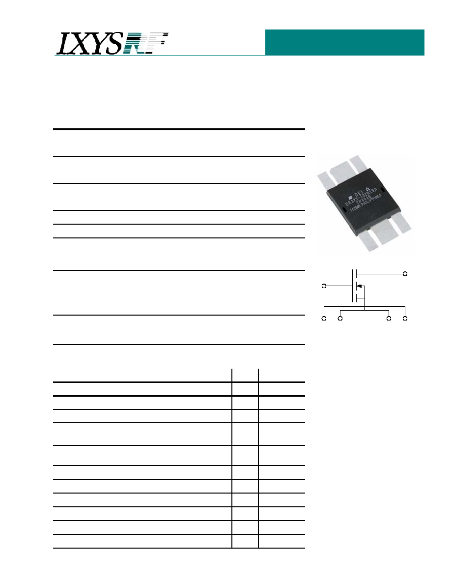
DRAIN
SG1
SG2
GATE
SD1
SD2

DE375-102N10A
RF Power MOSFET
Symbol Test
Conditions
Characteristic Values
(
T
J
= 25∞C unless otherwise specified)
min. typ.
max.
R
G
0.3
C
iss
2900
pF
C
oss
V
GS
= 0 V, V
DS
= 0.8 V
DSS(max)
,
f = 1 MHz
100
pF
C
rss
25
pF
T
d(on)
5
ns
T
on
V
GS
= 15 V, V
DS
= 0.8 V
DSS
I
D
= 0.5 I
DM
R
G
= 0.2
(External)
3
ns
T
d(off)
5
ns
T
off
8
ns
Q
g(on)
90
nC
Q
gs
V
GS
= 10 V, V
DS
= 0.5 V
DSS
I
D
= 0.5 I
D25
30
nC
Q
gd
40
nC
C
stray
Back Metal to any Pin
33
pF
Source-Drain Diode -
Characteristic Values
(
T
J
= 25∞C unless otherwise specified)
Symbol
Test Conditions
min. typ.
max.
I
S
V
GS
= 0 V
10
A
I
SM
Repetitive; pulse width limited by T
JM
80
A
V
SD
1.5
V
T
rr
200
ns
I
F
= I
S
, V
GS
= 0 V,
Pulse test, t
300 µs, duty cycle 2%
Q
RM
I
F
= I
S
, -di/dt = 100A/
µs,
V
R
= 100V
0.6
µC
I
RM
7
A
IXYS RF reserves the right to change limits, test conditions and dimensions.
IXYS RF MOSFETS are covered by one or more of the following U.S. patents:
4,835,592 4,850,072 4,881,106 4,891,686 4,931,844 5,017,508
5,034,796 5,049,961 5,063,307 5,187,117 5,237,481 5,486,715
5,381,025 5,640,045
(1) These parameters apply to the package, not individual MOSFET devices.
For detailed device mounting and installation instructions, see the "DE-
Series MOSFET Mounting Instructions" technical note on IXYS RF's web
site at www.ixysrf.com/Technical_Support/App_notes.html

DE375-102N10A
RF Power MOSFET
An IXYS Company
2401 Research Blvd., Suite 108
Fort Collins, CO USA 80526
970-493-1901 Fax: 970-493-1903
Email: deiinfo@directedenergy.com
Web: http://www.directedenergy.com
102N10A DE-SERIES SPICE Model
The DE-SERIES SPICE Model is illustrated in Figure 1. The model is an expan-
sion of the SPICE level 3 MOSFET model. It includes the stray inductive terms
L
G
, L
S
and L
D
. Rd is the R
DS(ON)
of the device, Rds is the resistive leakage term.
The output capacitance, C
OSS
, and reverse transfer capacitance, C
RSS
are mod-
eled with reversed biased diodes. This provides a varactor type response nec-
essary for a high power device model. The turn on delay and the turn off delay
are adjusted via Ron and Roff.
Figure 1 DE-SERIES SPICE Model
This SPICE model may be downloaded as a text file from the DEI web site at
www.directedenergy.com/spice.htm
Net List:
.SUBCKT 102N10A 10 20 30
* TERMINALS: D G S
* 1000 Volt 10 Amp 1.2 ohm N-Channel Power MOSFET
* REV.A 05-23-00
M1 1 2 3 3 DMOS L=1U W=1U
RON 5 6 0.5
DON 6 2 D1
ROF 5 7 .1
DOF 2 7 D1
D1CRS 2 8 D2
D2CRS 1 8 D2
CGS 2 3 3.0N
RD 4 1 1.5
DCOS 3 1 D3
RDS 1 3 5.0MEG
LS 3 30 .5N
LD 10 4 1N
LG 20 5 1N
.MODEL DMOS NMOS (LEVEL=3 VTO=3.0 KP=3.8)
.MODEL D1 D (IS=.5F CJO=1P BV=100 M=.5 VJ=.6 TT=1N)
.MODEL D2 D (IS=.5F CJO=400P BV=1000 M=.4 VJ=.6 TT=400N RS=10M)
.MODEL D3 D (IS=.5F CJO=900P BV=1000 M=.3 VJ=.4 TT=400N RS=10M)
.ENDS
Doc #9200-0223 Rev 6
© 2003 IXYS RF