
© 1997 IXYS All rights reserved
27
V
RSM
V
RRM
Type
V
V
1000
1000
DSEI 60-10A
Symbol
Test Conditions
Maximum Ratings
I
FRMS
T
VJ
= T
VJM
100
A
I
FAVM
¨
T
C
= 60
∞
C; rectangular, d = 0.5
60
A
I
FRM
t
P
< 10
µ
s; rep. rating, pulse width limited by T
VJM
800
A
I
FSM
T
VJ
= 45
∞
C;
t = 10 ms (50 Hz), sine
500
A
t = 8.3 ms (60 Hz), sine
540
A
T
VJ
= 150
∞
C;
t = 10 ms (50 Hz), sine
450
A
t = 8.3 ms (60 Hz), sine
480
A
i
2
dt
T
VJ
= 45
∞
C
t = 10 ms (50 Hz), sine
1250
A
2
s
t = 8.3 ms (60 Hz), sine
1200
A
2
s
T
VJ
= 150
∞
C;
t = 10 ms (50 Hz), sine
1000
A
2
s
t = 8.3 ms (60 Hz), sine
950
A
2
s
T
VJ
-40...+150
∞
C
T
VJM
150
∞
C
T
stg
-40...+150
∞
C
P
tot
T
C
= 25
∞
C
189
W
M
d
Mounting torque with screw M3
0.45/4
Nm/lb.in.
Mounting torque with screw M3.5
0.55/5
Nm/lb.in.
Weight
6
g
Symbol
Test Conditions
Characteristic Values
typ.
max.
I
R
T
VJ
= 25
∞
C
V
R
= V
RRM
3
mA
T
VJ
= 25
∞
C
V
R
= 0.8 ∑ V
RRM
0.5
mA
T
VJ
= 125
∞
C
V
R
= 0.8 ∑ V
RRM
14
mA
V
F
I
F
= 60 A;
T
VJ
= 150
∞
C
1.8
V
T
VJ
= 25
∞
C
2.3
V
V
T0
For power-loss calculations only
1.43
V
r
T
T
VJ
= T
VJM
6.1
m
R
thJC
0.66
K/W
R
thCK
0.2
K/W
R
thJA
35
K/W
t
rr
I
F
= 1 A; -di/dt = 200 A/
µ
s; V
R
= 30 V; T
VJ
= 25
∞
C
35
50
ns
I
RM
V
R
= 540 V;
I
F
= 60 A; -di
F
/dt = 480 A/
µ
s
32
36
A
L
0.05
µ
H; T
VJ
= 100
∞
C
Fast Recovery
DSEI 60
I
FAVM
= 60 A
Epitaxial Diode (FRED)
V
RRM
= 1000 V
t
rr
= 35 ns
¨
I
FAVM
rating includes reverse blocking losses at T
VJM
, V
R
= 0.8 V
RRM
, duty cycle d = 0.5
Data according to DIN/IEC 747
IXYS reserves the right to change limits, test conditions and dimensions
TO-247 AD
C
A
A = Anode, C = Cathode
C
C
A
Features
l
International standard package
JEDEC TO-247 AD
l
Planar passivated chips
l
Very short recovery time
l
Extremely low switching losses
l
Low I
RM
-values
l
Soft recovery behaviour
l
Epoxy meet UL 94V-0
Applications
l
Antiparallel diode for high frequency
switching devices
l
Anti saturation diode
l
Snubber diode
l
Free wheeling diode in converters
and motor control circuits
l
Rectifiers in switch mode power
supplies (SMPS)
l
Inductive heating and melting
l
Uninterruptible power supplies (UPS)
l
Ultrasonic cleaners and welders
Advantages
l
High reliability circuit operation
l
Low voltage peaks for reduced
protection circuits
l
Low noise switching
l
Low losses
l
Operating at lower temperature or
space saving by reduced cooling
96504A
© 1997 IXYS All rights reserved
28
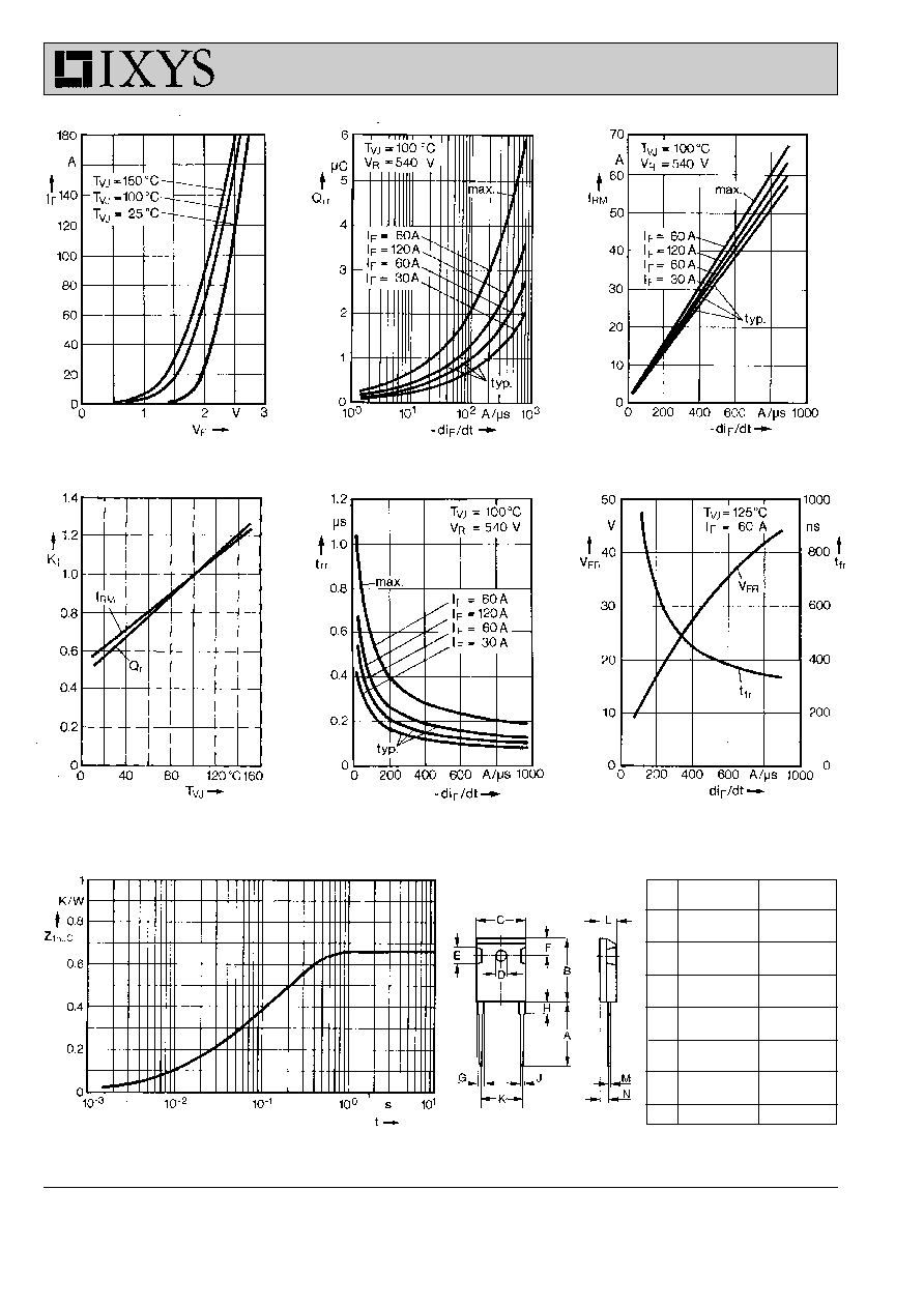
Fig. 1 Forward current
Fig. 2 Recovery charge versus -di
F
/dt.
Fig. 3 Peak reverse current versus
versus voltage drop.
-di
F
/dt.
Fig. 4 Dynamic parameters versus
Fig. 5 Recovery time versus -di
F
/dt.
Fig. 6 Peak forward voltage versus
junction temperature.
-di
F
/dt.
Fig. 7 Transient thermal impedance junction to case.
DSEI 60, 1000 V
Dim.
Millimeter
Inches
Min.
Max.
Min.
Max.
A
19.81 20.32
0.780
0.800
B
20.80 21.46
0.819
0.845
C
15.75 16.26
0.610
0.640
D
3.55
3.65
0.140
0.144
E
4.32
5.49
0.170
0.216
F
5.4
6.2
0.212
0.244
G
1.65
2.13
0.065
0.084
H
-
4.5
-
0.177
J
1.0
1.4
0.040
0.055
K
10.8
11.0
0.426
0.433
L
4.7
5.3
0.185
0.209
M
0.4
0.8
0.016
0.031
N
1.5
2.49
0.087
0.102
Dimensions