 | –≠–ª–µ–∫—Ç—Ä–æ–Ω–Ω—ã–π –∫–æ–º–ø–æ–Ω–µ–Ω—Ç: EV6R11S3 | –°–∫–∞—á–∞—Ç—å:  PDF PDF  ZIP ZIP |
Features
∑ Single chip for driving high/low side MOSFETs /
IGBTs
∑ High to low side isolation of 600V
∑ Common-mode dv/dt immunity of greater than
50V/nanosecond
∑ Undervoltage lockout
∑ Optimized power circuit layout
∑ High side bootstrap supply
∑ Sockets for freewheeling fast recovery diodes
(FREDS)
∑ Flexibility of power level utilization
∑ 5V compatible HCMOS input logic with hysterisis
∑ Protection from cross conduction of the half
bridge
∑ Simple, fast and low cost means of evaluation
and design
∑ Option for using IXDP630 with RC oscillator or
IXDP631 with crystal oscillator for improved dead
time accuracy.
∑ Three phase operation with the ability to attach
additional slave driver boards.
First Release
Copyright © IXYS CORPORATION 2003
Introduction
The EV6R11 KIT implements a single power phase-leg
circuit on a double-sided PCB, using the ISOSMART
TM
HALF BRIDGE DRIVER CHIPSET - IX6R11and IXDP630
dead time generator. This evaluation board includes an
assembled and tested PCB with two power devices. Just
follow the instructions in this document and connect the
board to the load and power.
Any power circuit is layout sensitive. The layout of this
PCB is a proven, working layout. The designer is invited
to duplicate this layout in his system, following the
evaluation of the driver chipset.
Most systems vary in their power level requirements and
therefore the power devices used. Due to this fact and
fluctuations in availability of power devices, the kit will not
always include the same power devices. The designer is
encouraged to use the power devices that are required for
his system. The devices that are enclosed serve only for
initial evaluation.
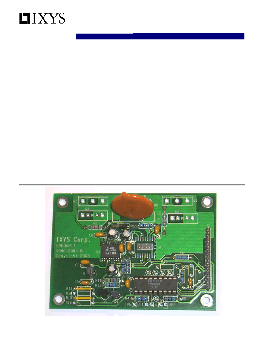
IX6R11 HALF BRIDGE DRIVER Evaluation Board
EV6R11
Figure 1: EV6R11 Assembled PCB With S3 Package
2
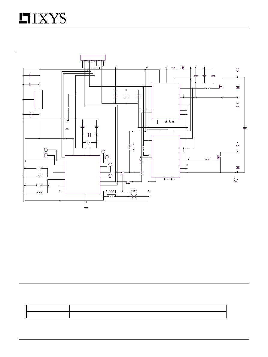
EV6R11 KIT
Figure 3: EV6R11 PCB Schematic
Schematic Diagram:
Ordering:
Schematic Notes:
This is a demonstration PCB and has been designed for flexibility and ease of use. The
schematic shows all options but does not mean the PCB is configured as such when ordered. The
PCB will be loaded with either the IX6R11S3 16 pin SOIC package (U3) OR the IX6R11S6 18 pin
SOIC package with heat sink tab (U4). The free-wheeling diodes, D2 and D3, are also not included
but can be installed if IGBTs are used.
EV6R11S3
PCB with IX6R11S3 16 pin SOIC IC package
EV6R11S6
PCB with IX6R11S6 18 pin SOIC IC package with heat tab
( Dead Timer )
U 2
IXD P630/631
R
1
Vc
c
18
S U
15
GN
D
9
SL
14
TU
13
TL
12
ENAT
6
RE SET (ac tiv e low)
8
S
3
ENAR
2
RC
I
N
/
X
T
L
I
N
10
OS
C
O
U
T
11
OUTEN A
7
ENAS
4
T
5
R L
16
R U
17
IX
6
R
11
S3
U 3
LGO
1
L S
2
VC
L
3
N/
C
4
N/
C
5
H S
6
VC
H
7
HGO
8
H S
9
N/
C
10
Vd
d
11
HI N
1 2
EN B
1 3
LI N
1 4
DG
15
L S
1 6
R 15 jum pered
R 16 open
D 1
U F-1007 DIC T
Y 1
XM/S M
L
O
A
D
Y
1
,
C6
F
O
R I
X
D
P
6
3
1
R
6
10K
U 1
LM78L05 AC Z
IN
3
OU
T
1
GN D
2
R8
1
K
R7
1
K
R 5 10K
R 4 10K
ENAS
ENAT
JP1
JP 2
I
X
6R
11
S
6
U 4
L S
1
LGO
2
VC
L
3
L S
4
N/
C
5
N/
C
6
H S
7
HGO
8
VC
H
9
H S
1 0
N/
C
11
N/
C
12
Vd
d
13
HI N
1 4
EN B
1 5
LI N
1 6
DG
17
L S
1 8
P1-1 GND
P1 pins
P1-4 Vdd supply line
P1-3 LIN
P1-2 HIN
P1-6 PWM IN
P1-5 ENB active low
P1-7 +5V for IXDB630
R 3
1K / 1M
R 9
10
P1
1
1
2
2
3
3
4
4
5
5
6
6
7
7
8
8
9
9
10
10
11
11
12
12
13
13
R1
0
4
9
.
9
C 4
. 1UF
P1-10 +VCL
P1-11 +VCL
C5 = 22 pF for IXDP631
C5 = 27 pF for IXDP630
R 13 jum pered
R 14 open
R1
2
4
.
0
2
K
R1
1
4
.
0
2
K
C 5
27p F (2 2pF )
C 6
22PF
Q2
IXF H7N 90Q
1
2
3
Q1
IXF H7N 90 Q
1
2
3
R 2
5.11
R 1
5.11
R
3
=
1M
f
or
IX
DP
63
1
R3
=
1
K
f
o
r
I
X
DP
6
3
0
+
C10
10 UF 35V
C1 1
. 1UF
D 3
D 2
TP 2
1
TP 6
1
TP3
1
TP 1
1
TP4
1
TP 5
1
+
C 1
10 UF 35V
C 9
. 1UF 1K V
+
C 7
10
U
F
35
V
C 8
. 1UF
P1-8 external 630 drive
P1-9 N/C
C 2
. 1UF
C 3
.01UF
LS GN D
TESTPOINT
1
Q1-D
TES TPOINT
1
DC BU S
TESTPOINT
1
Q2-S
TES TPOINT
1
P1-12 LS (VCL GND)
P1-13 LS (VCL GND)
Q3
2N 700 0
2
1
3
Q4
2N 7000
2
1
3
C12
. 1UF
C13
. 1UF

3
EV6R11 KIT
ASSEMBLY:
Figure 3 is a complete schematic diagram of the
design kit. This schematic indicates an applica-
tion using MOSFETs. When IGBTs are used,
freewheeling diodes (D2&D3) are typically
added.
To operate the PCB, simply solder the included
MOSFET power devices and C9 or install de-
vices specific to your application. Note gate drain
source pin orientation of power devices when
installing on the PCB. C9 has not been installed
due to its high profile and possible lead damage.
NOTES:
a) The ICs and Power devices are static sensi-
tive and require special handling.
b) Use any power device that is suitable for your
application. The PCB was designed to accept
devices with TO-247 or TO-264 packages. Two
IXYS power devices are included in the kit. D2
and D3 are required only if Q1 and Q2 are IGBTs,
and thus are not included in the kit. (A recom-
mendation for D2 & D3 is in the Bill of Materials).
c) Use any convenient method of interconnec-
tion at LS_GND, Q1-D, Q2-S, DC_BUS. The
hole spacing is 5.08mm and will fit most com-
mon terminal blocks. (A recommendation for a
connector that the PCB will accept is in the Bill
of Materials and is available from Digi-Key
among other sources).
d) For half bridge applications, insert a jumper
between Q1-D and Q2-S.
e) The gate resistors, R1 and R2, will depend on
the power device size that is used. 5.11 Ohm
resistors are installed and should work for most
applications.
f) IXDP630 dead time is provided by timing
components R3 and C5 and is fixed at roughly
1 microsecond. See the IXDP630 data sheet for
calculation and modification of the dead time
value. It must also be noted that dead time starts
to impact drive signals as drive frequency goes
up. Jitter is then produced as drive signal 'On'
time overlaps into dead time. A practical limit in
values are soon reached with timing compo-
nents R3 and C5 as they are adjusted to com-
pensate for the reduced period in drive frequency.
It is possible to 'overdrive' the IXDP630 with an
external clock signal applied to pin 10 to reduce
dead time even further than what is possible with
R3 and C5. To do this, remove R3, C5 from the
board and install a 50 Ohm load resistor at
position R10. Solder pads have been provided
at R10 to solder the ends of a coax cable directly
to the board. The IXDP630 can be driven in
excess of 50MHz.
g) The IXDP630 dead time generator is a 5V
HCMOS device. The addition of the IXDP630 on
the evaluation board is in part for convenience in
providing dual complementary drive signals. The
IXDP631 is a performance extension of the
IXDP630 and can be added as desired by the
user. However there is no part number available
for a IXDP631 loaded evaluation board and the
user must request IXDP631 samples separately.
Please note that threshold levels must be ob-
served when selecting the front end logic Vdd
supply voltage. To increase threshold level flex-
ibility, this PCB incorporates a level translation
circuit with Q3 and Q4. As configured, a three
terminal +5V regulator, U1, supplies power to
the IXDP630 and translator circuit which implies
that Vdd should be greater than 8V to prevent
regulator drop-out. Please note that this is only
one way to configure the board and was chosen
to provide a fast, easy way to get started during
the design stage.

4
EV6R11 KIT
Bill of Materials
Reference Qty. Description
Mfr.
Part #
U1
1
+5V regulator
National Semi.
LM78L05ACZ
U2
1
Dead time generator IC
IXYS
IXDP630
U3
1
16 pin Half Bridge Driver
IXYS
IX6R11S3
U4
1
18 pin Half bridge Driver
IXYS
IX6R11S6
D1
1
1A, 1000V high speed diode
Diodes Inc.
UF1007DICT
U2
1
18 pin socket
Assmann
A18-LC-TT
Q1, 2
2
High voltage power MOSFET
IXYS
IXFH7N90Q
Q3, 4
2
Switching MOSFET
Motorola
2N7000
R1, 2
2
5.11 ohm, 1/4 W resistors
R4, 5, 6
3
10k ohm, 1/4 W resistors
R3, 7, 8
3
1k ohm, 1/4 W resistors
R9
1
10 ohm, 1/4 W resistors
R11, 12
2
4.02k ohm 1/4 W resistors
R13, 15
2
Insulated wire jumpers
C1,7,10
3
10uF, 35V, aluminum electrolytic cap
Panasonic
C2,4,8,11,12,13
6
0.1uF, 50V, ceramic cap
Panasonic
C3
1
0.01uF, 50V, ceramic cap
C5
1
27pF, 50V, ceramic cap
Panasonic
C9
1
0.1uF, 1000V, ceramic cap
Sprague
10GAP10
P1
1
13 pin header connector
Berg
68000-236
NOT INCLUDED:
U2
1
Crystal based dead time generator
IXYS
IXDP631
D4, D5
2
12A, 1000V fast recovery diode
IXYS
DSEI12-10A
P2
1
4 pole terminal block
Altech Corp.
AKZ250/4
R3
1
1M ohm, 1/4 W IXDP631 osc load resistor
R10
1
50 ohm, 1/4 W load resistor
C5, 6
2
Crystal load capacitors, 22pF 50V ceramic
Panasonic
Y1
1
Crystal for IXDP631 operation
Pletronics
IXFH 7N90Q Power MOSFETS:
http://www.ixys.com/98645.pdf
The following list provides direct web links for the IXYS devices included with this PCB.
Please visit the IXYS web site at www.ixys.com for a complete overview of the entire IXYS product
line.
IX6R11 Half Bridge Driver IC:
http://www.ixys.com/99037.pdf
IXDP630 Digital Dead Time Generator:
http://www.ixys.com/98568.pdf
DATA SHEETS:

5
EV6R11 KIT
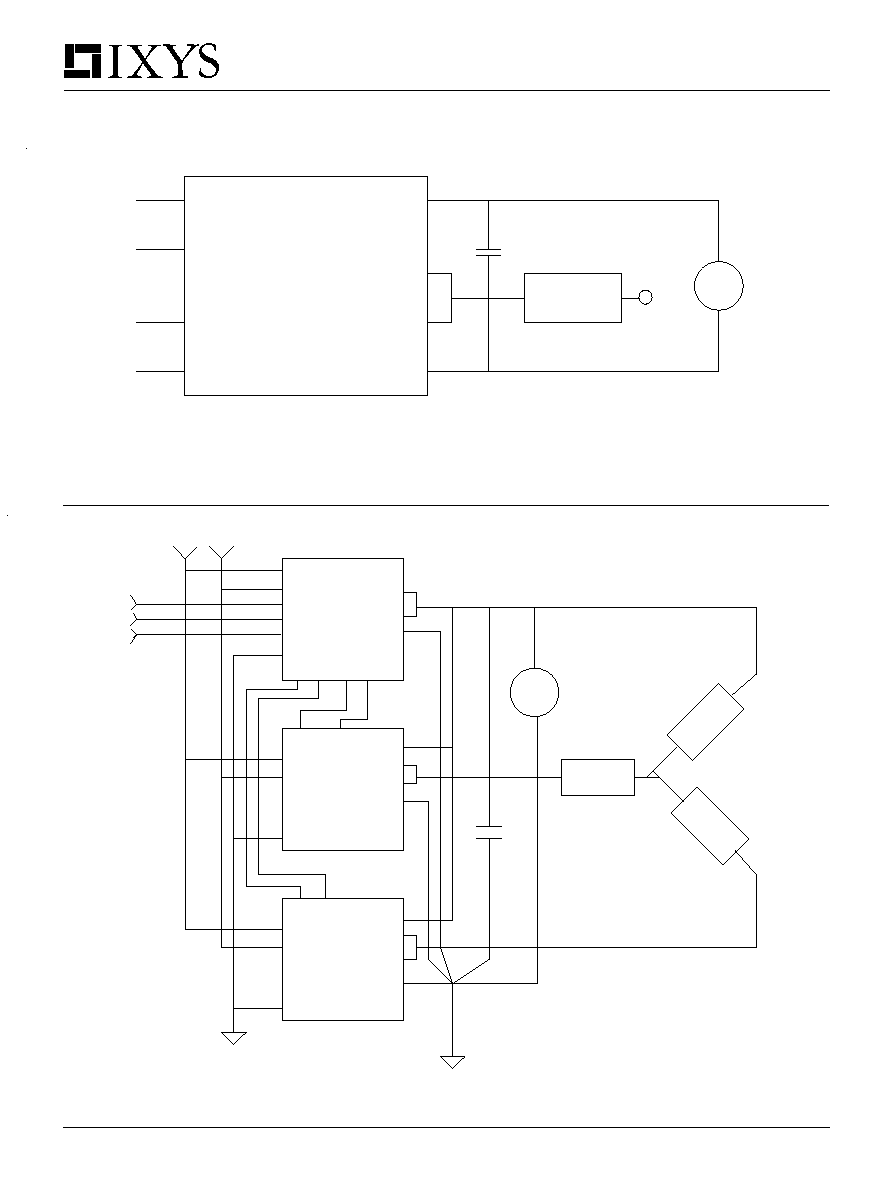
OPERATION:
For performance evaluation and power
system design please note the following:
a) The assembled board can be run with the
IXDP630 removed by applying complemen-
tary 5V square waves with proper "dead time"
to the input pins HIN (P1-2) and LIN (P1-3).
For standard IXDP630 operation, the
values of R3 and C5 have been listed on the
bill of materials. These values are for demon-
stration, which may not be appropriate for your
application and can be changed as needed.
For IXDP631 operation, load R3, C5, C6 with
the recommended load components as out-
lined in the IXDP630/631 data sheet along
with the crystal at the frequency of choice. R3
and C5 serve a dual purpose depending on
which dead timer is used.
The IXDP630 is hardwired for phase 'R'
operation, see 630/631 data sheet, with pins
OUTENA, ENAR, and RESET tied high.
PWM drive input signal for ' R' phase is ap-
plied to P1-6.
To add phases 'S' and/or 'T', enable
phases with jumpers at JP1 and/or JP2 and
apply PWM phase drive signals to TP5 and/or
TP6 taking the respective complementary
outputs from TP1 through TP4. Note that TP1-
TP6 are through-hole pads that have been
added to the board to serve as convenient
solder and/or test points.
b) The IX6R11 provides a wide range of
flexibility with its power supply requirements.
However, threshold levels must be observed
in the relationship between Vdd to HIN and
LIN when selecting power supply values in
the final design. Device propagation delays
can also be minimized by observing relative
values between supplies.
c) Be careful with ground connections. Avoid
ground loops. In general, connect the grounds
as shown in Figure 4 to minimize ground
bounce effects. This is particularly important
when three "High/Low side driver design kits"
are connected together with a single IXDP630
to form a three phase drive system, such as
that shown in Figure 5.
d) Before using the PCB at full power or at-
tempting a short circuit test, make sure that a
proper high voltage electrolytic capacitor is
connected between DC BUS and GND as
shown in Figure 4. The leads to this capacitor
should be as short as possible to minimize
any stray inductance.
e) Figure 4 shows the load terminated at point
A. This point could be connected to a number
of places depending on the application. For
example: Connection to ground will test the
high side device. Connection to DC BUS will
test the low side device. It could also be con-
nected to the center point of a capacitive
divider (UPS systems).
f) Figure 5 shows a three phase power system
implementation with a load configured in a Y
(star). It could also be configured in a DELTA
configuration. Please note the grounding
scheme. Cut the connection between "ground
plane 2" and "ground plane 4" on the compo-
nents side of the PCB and solder a 10 Ohm
resistor between these ground planes. The
GND of each board is terminated to a single
ground point.
6
EV6R11 KIT
Figure 5: EV6R11 Three Phase Configuration
Figure 4: Evaluation Board & Load Termination
LOAD
LS-GND
Q1-D
Q2-S
DC-BUS
A
+
DC
Supply
C1
.
.
.
+
-
GND P1-1
PWM P1-6
Vcl P1-10
Vdd P1-4
EVBD6R11
>
>
>
>
EVBD6
R
1
1
LO
AD
LO
AD
LOAD
DC BUS
LS-GND
Q1-D
Q2-S
EVBD6
R
1
1
Vdd
Vcl
R
GND
SL
TU
SU
TL
S
T
DC BUS
LS-GND
P1-2
DC BUS
LS-GND
P1-3
P1-3 P1-2
EVBD6
R
1
1
Q2-S
Q2-S
Q1-D
Q1-D
R phase
S phase
T phase
.
.
.
.
.
.
.
. .
+
+
-
C1
Vcl
Vcl
Vdd
Vdd
GND
GND
LS-GND
.
.
GND
Vdd
Vcl
.
.
.
.
R drive
S drive
T drive
DC
Supply
EV6R11
EV6R11
EV6R11
EV6R11
7
EV6R11 KIT
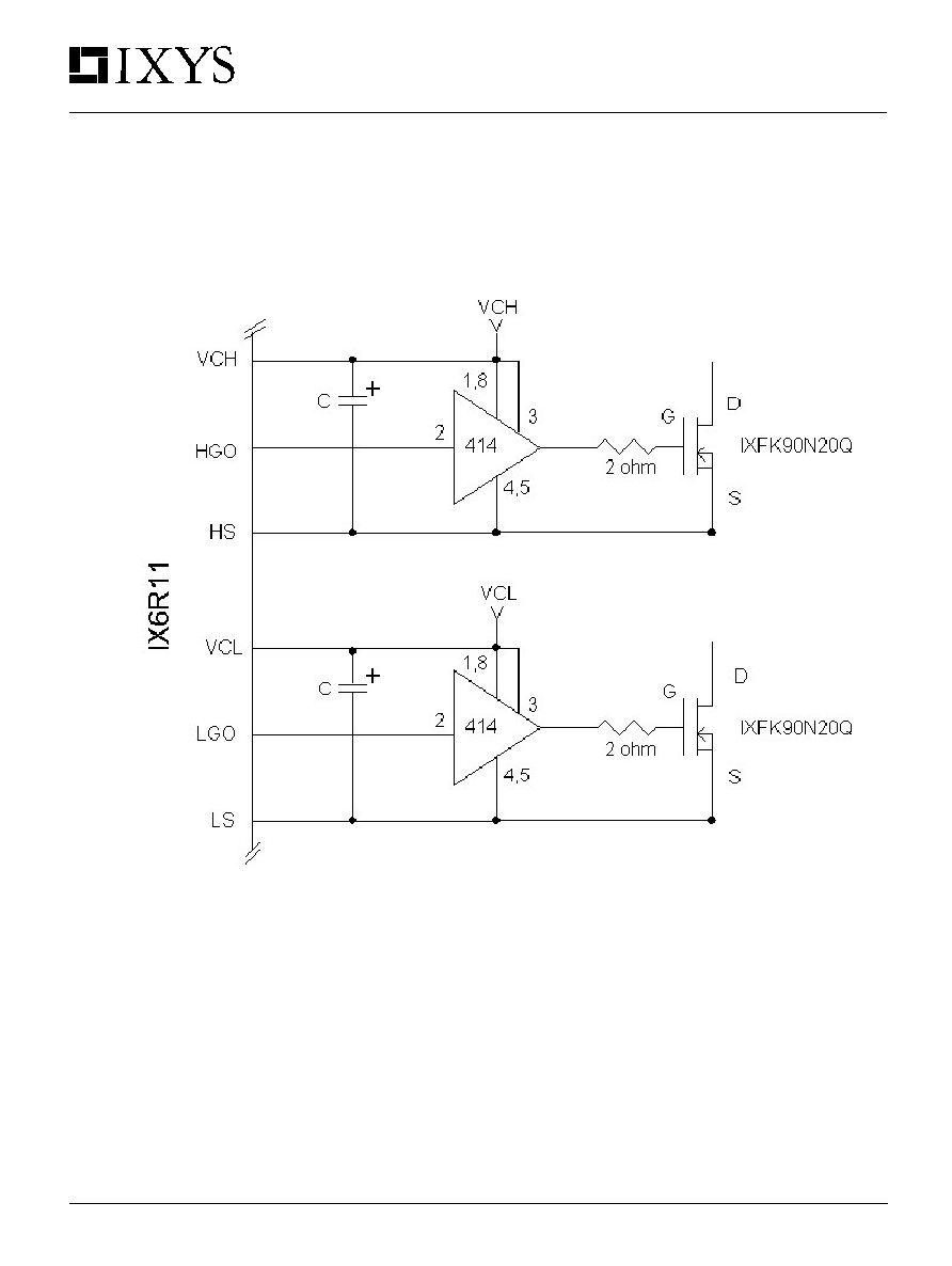
Figure 6: Boosting the IX6R11 outputs for larger MOSFETs.
With the addition of High Current MOSFET Drivers on the outputs, the IX6R11's typical 6A peak output current
capability can be "boosted" to drive the latest IXYS MOSFETS & IGBTs. Figure 6 shows the addition of two
IXDD414's. These are CMOS high-speed MOSFET drivers that have a 14A Peak Output Drive Capability, allowing
the IX6R11 to drive a pair of IXFK90N20Q 90A/200V Power MOSFETs. The 2 Ohm gate resistors shown should
be Non-Inductive High Performance Film resistors such at those available from Caddock. Particular attention also
needs to be paid to Suppy By-passing, Grounding, and minimizing the Output Lead Inductance when designing such
a high power circuit layout.
DS99102(10/03)