© 2005 IXYS All rights reserved
515
1 - 2
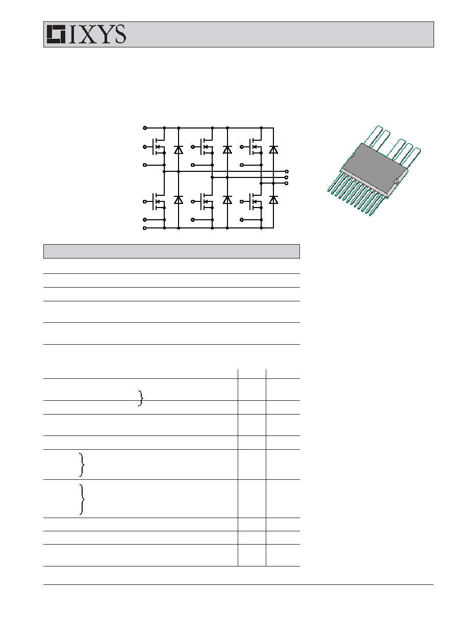
GWM 220-004P3
Three phase full bridge
with Trench MOSFETs
in DCB isolated high current package
Applications
AC drives
∑ in automobiles
- electric power steering
- starter generator
∑ in industrial vehicles
- propulsion drives
- fork lift drives
∑ in battery supplied equipment
Features
∑ MOSFETs in trench technology:
- logic level gate control
- low R
DSon
- optimized intrinsic reverse diode
∑ package:
- high level of integration
- high current capability
- auxiliary terminals for MOSFET control
- terminals for soldering or welding
connections
- isolated DCB ceramic base plate
with optimized heat transfer
V
DSS
= 40 V
R
DSon
= 2.0 m
I
D25
= 190 A
IXYS reserves the right to change limits, test conditions and dimensions.
MOSFETs
Symbol
Conditions
Maximum Ratings
V
DSS
T
VJ
= 25∞C to 150∞C
40
V
V
GS
±20
V
I
D25
T
C
= 25∞C
190
A
I
D90
T
C
= 90∞C
145
A
I
F25
T
C
= 25∞C (diode)
125
A
I
F90
T
C
= 90∞C (diode)
80
A
Symbol
Conditions
Characteristic Values
(T
VJ
= 25
∞C, unless otherwise specified)
min.
typ.
max.
R
DSon
on chip level at
T
VJ
= 25∞C
2.0
2.6 m
V
GS
= 10 V
T
VJ
= 125∞C
3.2
m
V
GSth
V
DS
= 20 V;
I
D
= 1 mA
2
4
V
I
DSS
V
DS
= V
DSS
;
V
GS
= 0 V; T
VJ
= 25∞C
1
µA
T
VJ
= 125∞C
0.1
mA
I
GSS
V
GS
= ±20 V; V
DS
= 0 V
0.2
µA
Q
g
94
nC
Q
gs
18
nC
Q
gd
29
nC
t
d(on)
40
ns
t
r
85
ns
t
d(off)
140
ns
t
f
90
ns
V
F
(diode) I
F
= 110 A; V
GS
= 0 V
1.0
1.6
V
t
rr
(diode) I
F
= 20 A; -di/dt = 100 A/µs; V
DS
= 20 V
70
ns
R
thJC
0.85 K/W
R
thJH
with heat transfer paste
1.1
K/W
V
GS
= 10 V; V
DS
= 14 V; I
D
= 25 A
V
GS
= 10 V; V
DS
= 30 V;
I
D
= 25 A; R
G
= 10
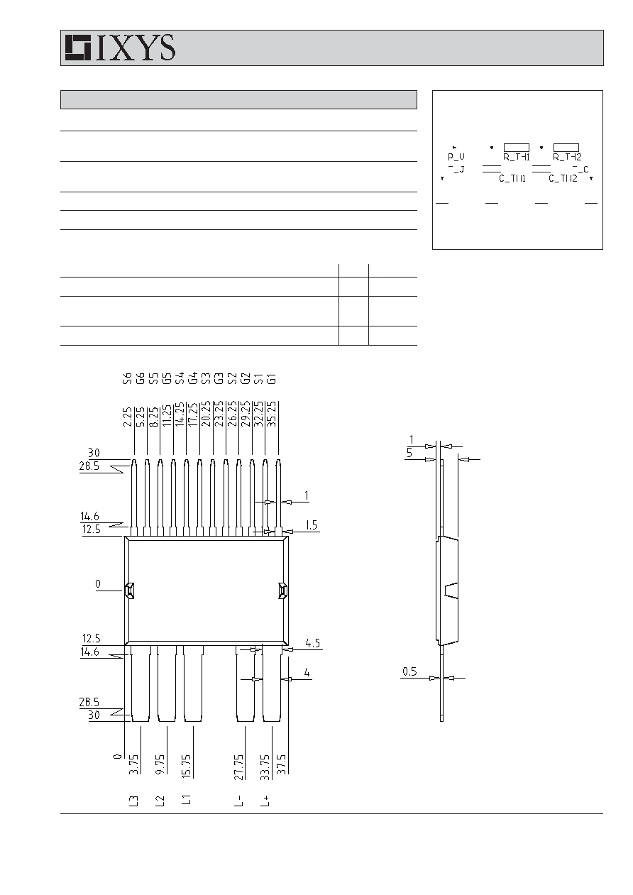
L +
G1
S1
G2
S2
L -
G3
S3
G4
S4
G5
S5
G6
S6
L1
L2
L3
Preliminary data
© 2005 IXYS All rights reserved
515
2 - 2
GWM 220-004P3
Dimensions in mm (1 mm = 0.0394")
Component
Symbol
Conditions
Maximum Ratings
I
RMS
per pin in main current paths (P+, N-, L
1
, L
2
, L
3
)
300
A
may be additionally limited by external connections
T
VJ
-40...+175
∞C
T
stg
-55...+125
∞C
V
ISOL
I
ISOL
1 mA; 50/60 Hz; t = 1 min
1000
V~
F
C
Mounting force with clip
50 - 250
N
Symbol
Conditions
Characteristic Values
(T
VJ
= 25
∞C, unless otherwise specified)
min.
typ.
max.
R
pin to chip
0.6
m
C
P
coupling capacity between shorted
160
pF
pins and mounting tab in the case
Weight
typ.
25
g
Equivalent Circuits for Simulation
Thermal Response
junction - case (typ.)
C
th1
= 0.039 J/K; R
th1
= 0.28 K/W
C
th2
= 0.069 J/K; R
th2
= 0.57 K/W