1 - 2
© 2000 IXYS All rights reserved
Symbol
Test Conditions
Maximum Ratings
V
DSS
T
J
= 25
∞
C to 150
∞
C
300
V
V
DGR
T
J
= 25
∞
C to 150
∞
C; R
GS
= 1 M
W
300
V
V
GS
Continuous
±
20
V
V
GSM
Transient
±
30
V
I
D25
T
C
= 25
∞
C
40
A
I
DM
T
C
= 25
∞
C, pulse width limited by T
JM
160
A
I
AR
T
C
= 25
∞
C
40
A
E
AR
T
C
= 25
∞
C
30
mJ
E
AS
T
C
= 25
∞
C
1.0
J
dv/dt
I
S
£
I
DM
, di/dt
£
100 A/
m
s, V
DD
£
V
DSS
,
5
V/ns
T
J
£
150
∞
C, R
G
= 2
W
P
D
T
C
= 25
∞
C
300
W
T
J
-55 ... +150
∞
C
T
JM
150
∞
C
T
stg
-55 ... +150
∞
C
T
L
1.6 mm (0.062 in.) from case for 10 s
300
∞
C
M
d
Mounting torque
1.13/10 Nm/lb.in.
Weight
TO-247
6
g
TO-268
4
g
TO-247 AD (IXFH)
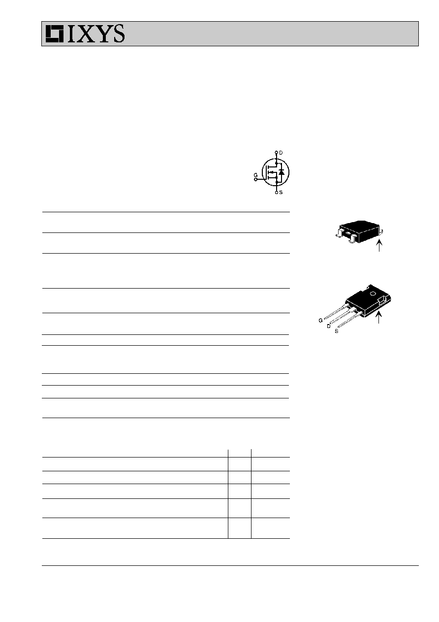
G = Gate
D = Drain
S = Source
TAB = Drain
(TAB)
98504A (6/99)
Symbol
Test Conditions
Characteristic Values
(T
J
= 25
∞
C, unless otherwise specified)
Min. Typ.
Max.
V
DSS
V
GS
= 0 V, I
D
=
250 m
A
300
V
V
GS(th)
V
DS
= V
GS
, I
D
= 4 mA
2.0
4
V
I
GSS
V
GS
=
±
20 V
DC
, V
DS
= 0
±
100
nA
I
DSS
V
DS
= V
DSS
T
J
= 25
∞
C
25
m
A
V
GS
= 0 V
T
J
= 125
∞
C
1
mA
R
DS(on)
V
GS
= 10 V, I
D
= 0.5 I
D25
80
m
W
Pulse test, t
£
300
m
s, duty cycle d
£
2 %
Preliminary data sheet
TO-268 (IXFT) Case Style
(TAB)
G
S
HiPerFET
TM
Power MOSFETs
Q-Class
N-Channel Enhancement Mode
Avalanche Rated, High dv/dt, Low Q
g
V
DSS
= 300 V
I
D25
= 40 A
R
DS(on)
= 80 m
W
t
rr
£
250 ns
IXFH 40N30Q
IXFT 40N30Q
IXYS reserves the right to change limits, test conditions, and dimensions.
Features
∑ IXYS advanced low Q
g
process
∑ International standard packages
∑ Low gate charge and capacitance
- easier to drive
- faster switching
∑ Low R
DS (on)
∑ Unclamped Inductive Switching (UIS)
rated
∑ Molding epoxies meet UL
94
V-0
flammability classification
Advantages
∑ Easy to mount
∑ Space savings
∑ High power density
2 - 2
© 2000 IXYS All rights reserved
IXFH 40N30Q
IXFT 40N30Q
Symbol
Test Conditions
Characteristic Values
(T
J
= 25
∞
C, unless otherwise specified)
Min.
Typ.
Max.
g
fs
V
DS
= 10 V; I
D
= 0.5 I
D25
, pulse test
22
30
S
C
iss
3100
pF
C
oss
V
GS
= 0 V, V
DS
= 25 V, f = 1 MHz
650
pF
C
rss
150
pF
t
d(on)
20
ns
t
r
V
GS
= 10 V, V
DS
= 0.5 V
DSS
, I
D
= 0.5 I
D25
35
ns
t
d(off)
R
G
= 1.5
W
(External)
40
ns
t
f
12
ns
Q
g(on)
95
140
nC
Q
gs
V
GS
= 10 V, V
DS
= 0.5 V
DSS
, I
D
= 0.5 I
D25
25
35
nC
Q
gd
54
70
nC
R
thJC
0.42
K/W
R
thCK
(TO-247)
0.25
K/W
Source-Drain Diode
Characteristic Values
(T
J
= 25
∞
C, unless otherwise specified)
Symbol
Test Conditions
min.
typ.
max.
I
S
V
GS
= 0 V
40
A
I
SM
Repetitive;
160
A
V
SD
I
F
= I
S
, V
GS
= 0 V,
1.5
V
Pulse test, t
£
300
m
s, duty cycle d
£
2 %
t
rr
250
ns
Q
RM
I
F
= I
S
-di/dt = 100 A/
m
s, V
R
= 100 V
0.85
m
C
I
RM
8
A
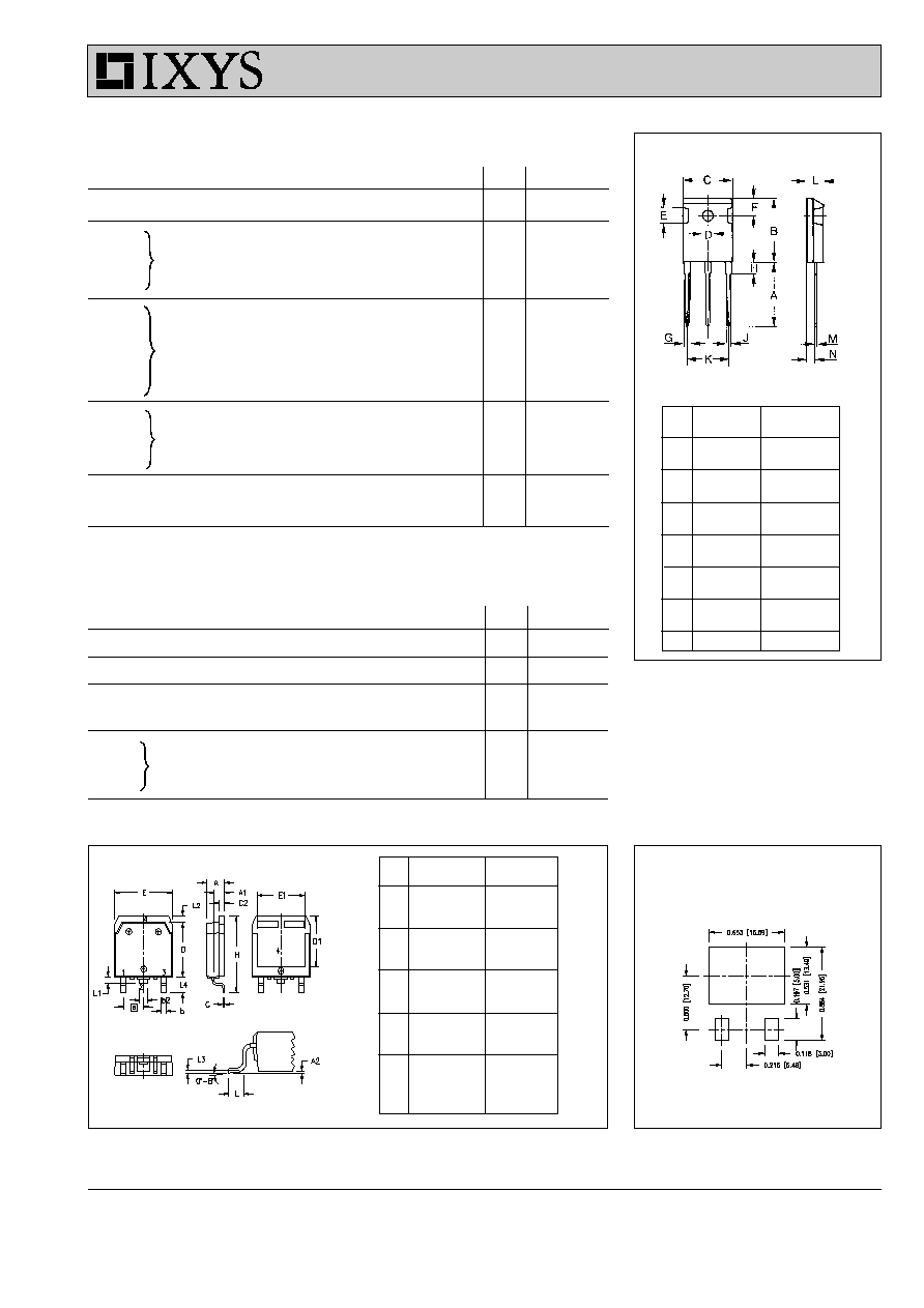
TO-247 AD (IXFH) Outline
Dim. Millimeter
Inches
Min.
Max.
Min.
Max.
A
19.81 20.32
0.780 0.800
B
20.80 21.46
0.819 0.845
C
15.75 16.26
0.610 0.640
D
3.55
3.65
0.140 0.144
E
4.32
5.49
0.170 0.216
F
5.4
6.2
0.212 0.244
G
1.65
2.13
0.065 0.084
H
-
4.5
-
0.177
J
1.0
1.4
0.040 0.055
K
10.8
11.0
0.426 0.433
L
4.7
5.3
0.185 0.209
M
0.4
0.8
0.016 0.031
N
1.5
2.49
0.087 0.102
Dim.
Millimeter
Inches
Min.
Max.
Min.
Max.
A
4.9
5.1
.193
.201
A
1
2.7
2.9
.106
.114
A
2
.02
.25
.001
.010
b
1.15
1.45
.045
.057
b
2
1.9
2.1
.75
.83
C
.4
.65
.016
.026
D
13.80
14.00
.543
.551
E
15.85
16.05
.624
.632
E
1
13.3
13.6
.524
.535
e 5.45 BSC .215 BSC
H
18.70
19.10
.736
.752
L
2.40
2.70
.094
.106
L1
1.20
1.40
.047
.055
L2
1.00
1.15
.039
.045
L3 0.25 BSC .010 BSC
L4
3.80
4.10
.150
.161
TO-268AA (D
3
PAK)
Min. Recommended Footprint
IXYS MOSFETS and IGBTs are covered by one or more of the following U.S. patents:
4,835,592
4,881,106
5,017,508
5,049,961
5,187,117
5,486,715
4,850,072
4,931,844
5,034,796
5,063,307
5,237,481
5,381,025