DRAFT(IXTH60N30P)
© 2004 IXYS All rights reserved
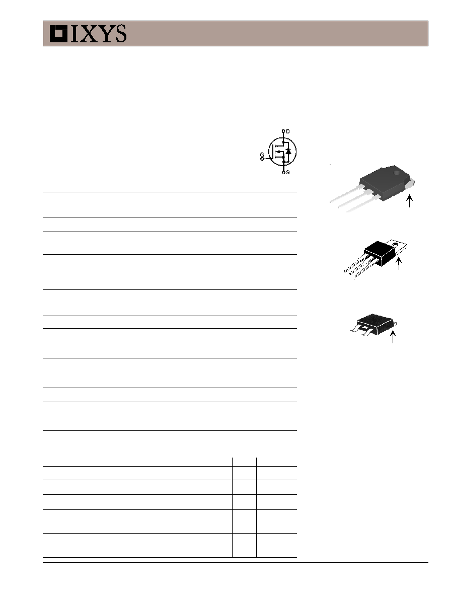
G
D
S
(TAB)
G
S
(TAB)
Symbol
Test Conditions
Maximum Ratings
V
DSS
T
J
= 25
°C to 175°C
200
V
V
DGR
T
J
= 25
°C to 175°C; R
GS
= 1 M
200
V
V
GSM
±20
V
I
D25
T
C
= 25
°C
50
A
I
DM
T
C
= 25
°C, pulse width limited by T
JM
120
A
I
AR
T
C
= 25
°C
50
A
E
AR
T
C
= 25
°C
30
mJ
E
AS
T
C
= 25
°C
1.0
J
dv/dt
I
S
I
DM
, di/dt
100 A/µs, V
DD
V
DSS
,
10
V/ns
T
J
150°C, R
G
= 10
P
D
T
C
= 25
°C
360
W
T
J
-55 ... +175
°C
T
JM
175
°C
T
stg
-55 ... +125
°C
T
L
1.6 mm (0.062 in.) from case for 10 s
300
°C
Maximum tab temperature for soldering
260
°C
TO-263 package for 10s
M
d
Mounting torque
(TO-3P / TO-220)
1.13/10 Nm/lb.in.
Weight
TO-3P
5.5
g
TO-220
4
g
TO-263
3
g
G = Gate
D = Drain
S = Source
TAB = Drain
DS99156A(04/04)
Symbol
Test Conditions
Characteristic Values
(T
J
= 25
°C, unless otherwise specified)
Min. Typ.
Max.
V
DSS
V
GS
= 0 V, I
D
= 250
µA
200
V
V
GS(th)
V
DS
= V
GS
, I
D
= 250
µA
2.5
5.0
V
I
GSS
V
GS
=
±20 V
DC
, V
DS
= 0
±100
nA
I
DSS
V
DS
= V
DSS
25
µA
V
GS
= 0 V
T
J
= 150
°C
250
µA
R
DS(on)
V
GS
= 10 V, I
D
= I
T
50
60
m
Pulse test, t
300 µs, duty cycle d 2 %
PolarHT
TM
Power MOSFET
N-Channel Enhancement Mode
Features
International standard packages
Unclamped Inductive Switching (UIS)
rated
Low package inductance
- easy to drive and to protect
Advantages
Easy to mount
Space savings
High power density
PolarHT
TM
DMOS transistors
utilize proprietary designs and
process. US patent is pending.
TO-263 (I
XTA)
TO-220 (I
XTP)
D
(TAB)
G
S
IXTQ 50N20P
IXTA 50N20P
IXTP 50N20P
V
DSS
= 200 V
I
D25
= 50 A
R
DS(on)
= 60 m
TO-3P (I
XTQ)
Preliminary Data Sheet
IXYS reserves the right to change limits, test conditions, and dimensions.
IXTA 50N20P IXTP 50N20P
IXTQ 50N20P
IXYS MOSFETs and IGBTs are covered by one or more
4,850,072
4,931,844
5,034,796
5,063,307
5,237,481
5,381,025
6,404,065B1 6,162,665
6,534,343
6,583,505
of the following U.S. patents:
4,835,592
4,881,106
5,017,508
5,049,961
5,187,117
5,486,715
6,306,728B1
6,259,123B1 6,306,728B1 6,683,344
Symbol
Test Conditions Characteristic Values
(T
J
= 25
°C, unless otherwise specified)
Min.
Typ.
Max.
g
fs
V
DS
= 10 V; I
D
= 50 A pulse test
12
23
S
C
iss
2250
pF
C
oss
V
GS
= 0 V, V
DS
= 25 V, f = 1 MHz
500
pF
C
rss
125
pF
t
d(on)
26
ns
t
r
V
GS
= 10 V, V
DS
= 0.5 V
DSS
, I
D
= I
T
35
ns
t
d(off)
R
G
= 10
(External)
70
ns
t
f
30
ns
Q
g(on)
70
nC
Q
gs
V
GS
= 10 V, V
DS
= 0.5 V
DSS
, I
D
= I
T
17
nC
Q
gd
37
nC
R
thJC
0.42 K/W
R
thCK
(TO-3P)
0.21
K/W
(TO-220)
0.25
K/W
Source-Drain Diode Characteristic Values
(T
J
= 25
°C, unless otherwise specified)
Symbol
Test Conditions
Min.
typ.
Max.
I
S
V
GS
= 0 V
50
A
I
SM
Repetitive
120
A
V
SD
I
F
= I
S
, V
GS
= 0 V,
1.5
V
Pulse test, t
300 µs, duty cycle d 2 %
t
rr
I
F
= 25 A
180
ns
-di/dt = 100 A/
µs
Q
RM
V
R
= 100 V
2.0
µC
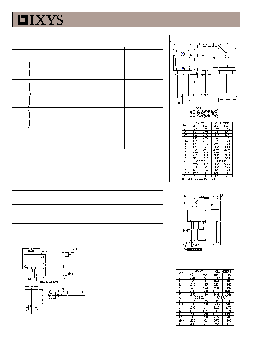
TO-3P (IXTQ) Outline
Pins: 1 - Gate
2 - Drain
TO-220 (IXTA) Outline
Dim.
Millimeter
Inches
Min.
Max.
Min.
Max.
A
4.06
4.83
.160
.190
A1
2.03
2.79
.080
.110
b
0.51
0.99
.020
.039
b2
1.14
1.40
.045
.055
c
0.46
0.74
.018
.029
c2
1.14
1.40
.045
.055
D
8.64
9.65
.340
.380
D1
7.11
8.13
.280
.320
E
9.65
10.29
.380
.405
E1
6.86
8.13
.270
.320
e
2.54
BSC
.100
BSC
L
14.61
15.88
.575
.625
L1
2.29
2.79
.090
.110
L2
1.02
1.40
.040
.055
L3
1.27
1.78
.050
.070
L4
0
0.38
0
.015
R
0.46
0.74
.018
.029
TO-263 (IXTP) Outline
Notes: Test current I
T
= 50 A.
© 2004 IXYS All rights reserved
IXTA 50N20P IXTP 50N20P
IXTQ 50N20P
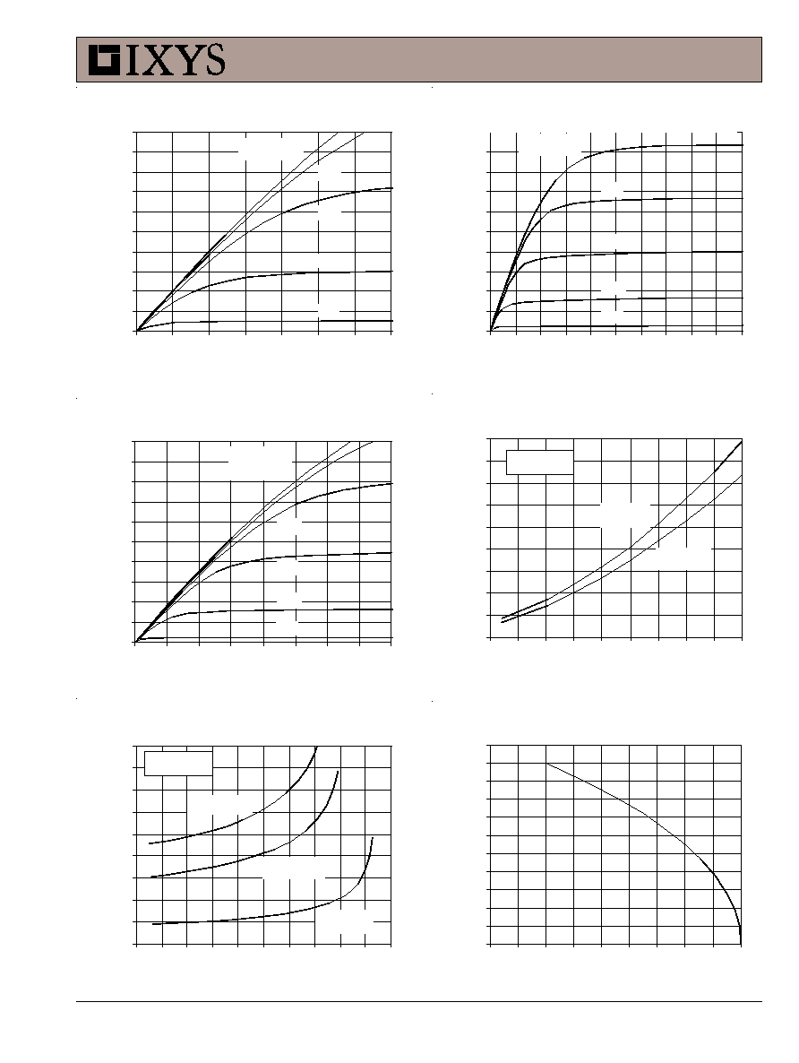
Fig . 1. Ou tp u t C h ar acte r is tics
@ 25
º
C
0
5
10
15
20
25
30
35
40
45
50
0
0.5
1
1. 5
2
2. 5
3
3. 5
V
D S
- V olts
I
D
- A
m
peres
V
GS
= 10V
7V
6V
8V
9V
Fig . 2. Exte n d e d Ou tp u t C h ar acte r is tics
@ 25
º
C
0
10
20
30
40
50
60
70
80
90
100
0
2
4
6
8
10
12
14
16
18
20
V
D S
- V olts
I
D
- A
m
peres
V
GS
= 10V
7V
6V
8V
9V
Fig . 3. Ou tp u t C h ar acte r is tics
@ 150
º
C
0
5
10
15
20
25
30
35
40
45
50
0
1
2
3
4
5
6
7
8
V
D S
- V olts
I
D
- A
m
peres
V
GS
= 10V
9V
5V
6V
7V
8V
Fig . 4. R
D S(on
)
No r m aliz e d to 0.5 I
D 25
V alu e vs . Ju n ctio n T e m p e r atu r e
0.4
0.7
1
1.3
1.6
1.9
2.2
2.5
2.8
3.1
-50
-25
0
25
50
75
100
125
150
175
T
J
- Degrees Centigrade
R
D
S
( o n )
- No
rm
a
l
i
z
e
d
I
D
= 50A
I
D
= 25A
V
GS
= 10V
Fig . 5. R
D S(o n)
No r m aliz e d to
0.5 I
D 25
V alu e vs . I
D
0. 6
1
1. 4
1. 8
2. 2
2. 6
3
3. 4
3. 8
4. 2
0
10
20
30
40
50
60
70
80
90
100
I
D
- A mperes
R
D
S
( o n )
- Norm
al
i
z
ed
T
J
= 125ºC
T
J
= 25ºC
V
GS
= 10V
T
J
= 175ºC
Fig . 6. Dr ain Cu r r e n t vs . C as e
T e m p e r atu r e
0
5
10
15
20
25
30
35
40
45
50
55
-50
-25
0
25
50
75
100
125
150
175
T
C
- Degrees Centigrade
I
D
- A
m
peres
IXYS reserves the right to change limits, test conditions, and dimensions.
IXTA 50N20P IXTP 50N20P
IXTQ 50N20P
IXYS MOSFETs and IGBTs are covered by one or more
4,850,072
4,931,844
5,034,796
5,063,307
5,237,481
5,381,025
6,404,065B1 6,162,665
6,534,343
6,583,505
of the following U.S. patents:
4,835,592
4,881,106
5,017,508
5,049,961
5,187,117
5,486,715
6,306,728B1
6,259,123B1 6,306,728B1 6,683,344
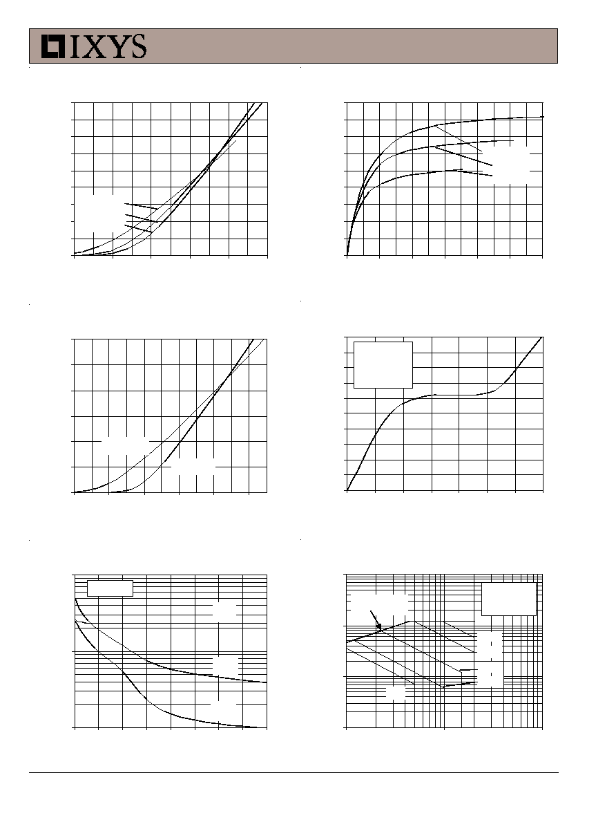
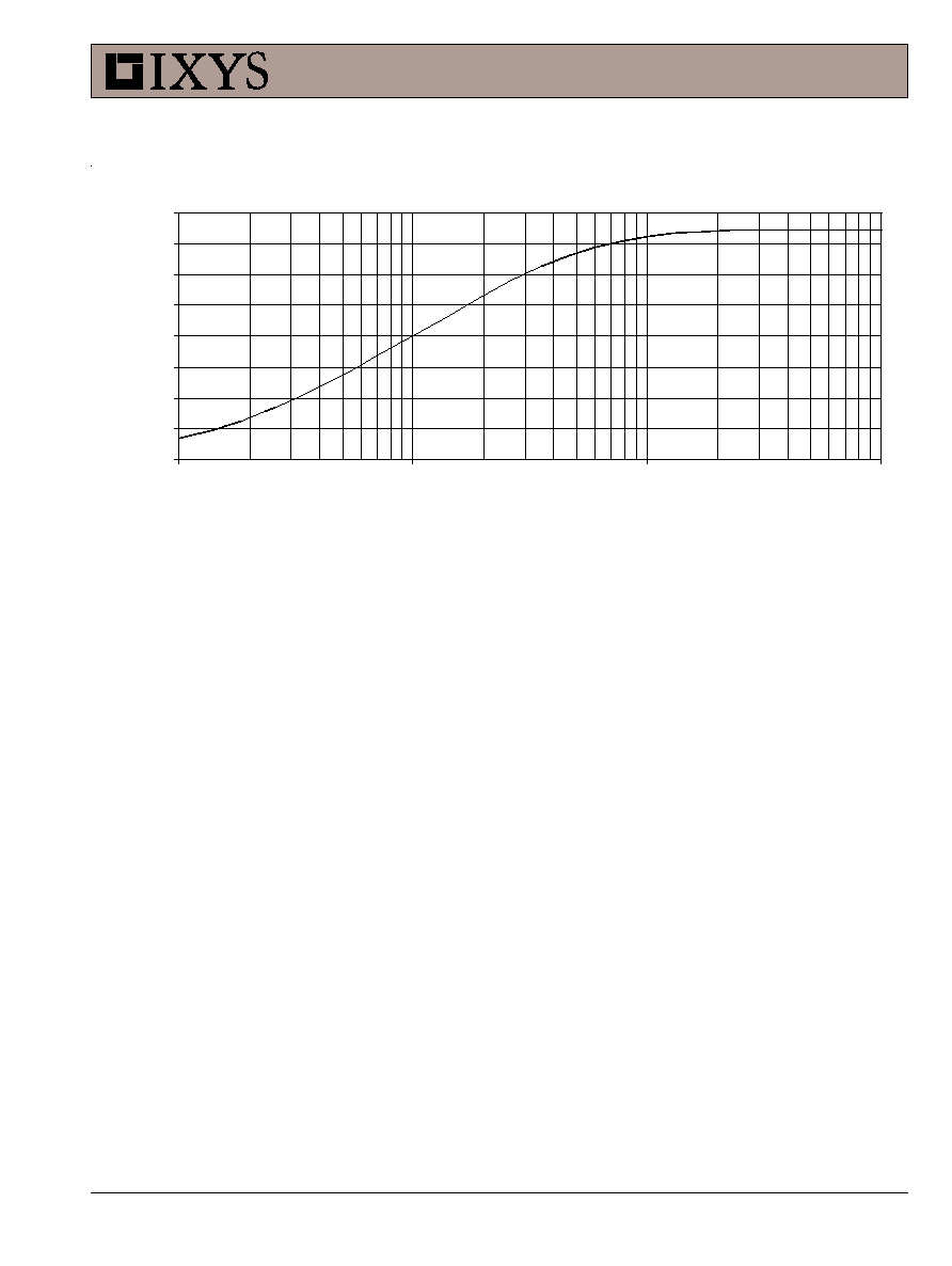
Fig . 7. In p u t A d m ittan ce
0
10
20
30
40
50
60
70
80
90
5
6
7
8
9
10
V
G S
- V olts
I
D
- A
m
peres
T
J
= 150ºC
25ºC
-40ºC
Fig . 8. T r an s co n d u ctan ce
0
4
8
12
16
20
24
28
32
36
0
20
40
60
80
100
120
I
D
- A mperes
g
f s
- S
i
emens
T
J
= -40ºC
25ºC
150ºC
Fig . 9. So u r ce C u r r e n t vs .
So u r ce -T o -Dr ain V o ltag e
0
25
50
75
100
125
150
0.4
0.6
0. 8
1
1. 2
1. 4
V
S D
- V olts
I
S
- A
m
peres
T
J
= 150ºC
T
J
= 25ºC
Fig . 10. Gate C h ar g e
0
1
2
3
4
5
6
7
8
9
10
0
10
20
30
40
50
60
70
Q
G
- nanoCoulombs
V
G S
- Vol
t
s
V
D S
= 100V
I
D
= 25A
I
G
= 10m A
Fig . 11. Cap acitan ce
100
1000
10000
0
5
10
15
20
25
30
35
40
V
D S
- V olts
C
apacitance - picoFarads
C is s
C os s
C rss
f = 1MH z
Fig . 12. Fo r w ar d -Bias
Safe Op e r atin g A r e a
1
10
100
1000
10
100
1000
V
D S
- V olts
I
D
- A
m
peres
100µs
1m s
D C
T
J
= 175ºC
T
C
= 25ºC
R
D S(on)
Lim it
10m s
25µs
© 2004 IXYS All rights reserved
IXTA 50N20P IXTP 50N20P
IXTQ 50N20P
Fig . 1 3 . M a x im u m T r a n s ie n t T h e r m a l Re s is t a n c e
0 . 0 5
0 . 1 0
0 . 1 5
0 . 2 0
0 . 2 5
0 . 3 0
0 . 3 5
0 . 4 0
0 . 4 5
1
1 0
1 0 0
1 0 0 0
Pu ls e W id th - m illis e c o n d s
R
( t h ) J
C
-
º
C /
W