
© 2000 IXYS All rights reserved
1 - 4
031
IXYS reserves the right to change limits, test conditions and dimensions.
Features
∑ High Voltage BIMOSFET
TM
- substitute for high voltage MOSFETs
with significantly lower voltage drop
- fast switching for high frequency
operation
- reverse conduction capability
∑ ISOPLUS i4-PAC
TM
high voltage package
- isolated back surface
- enlarged creepage towards heatsink
- enlarged creepage between high
voltage pins
- application friendly pinout
- high reliability
- industry standard outline
Applications
∑ switched mode power supplies
∑ DC-DC converters
∑ resonant converters
∑ lamp ballasts
∑ laser generators, x ray generators
IGBT
Symbol
Conditions
Maximum Ratings
V
CES
T
VJ
= 25∞C to 150∞C
IXBF 9N140
1400
V
IXBF 9N160
1600
V
V
GES
±
20
V
I
C25
T
C
= 25∞C
7
A
I
C90
T
C
= 90∞C
4
A
I
CM
V
GE
= 15/0 V; R
G
= 100
W
; T
VJ
= 125∞C
12
A
V
CEK
RBSOA, Clamped inductive load; L = 100 µH
0.8V
CES
P
tot
T
C
= 25∞C
70
W
Symbol
Conditions
Characteristic Values
(T
VJ
= 25
∞
C, unless otherwise specified)
min.
typ.
max.
V
CE(sat)
I
C
= 5 A; V
GE
= 15 V; T
VJ
= 25∞C
4.9
7
V
T
VJ
= 125∞C
5.6
V
V
GE(th)
I
C
= 0.5 mA; V
GE
= V
CE
4
8
V
I
CES
V
CE
= 0.8V
CES
;
V
GE
= 0 V; T
VJ
= 25∞C
0.1
mA
T
VJ
= 125∞C
0.1
mA
I
GES
V
CE
= 0 V; V
GE
=
±
20 V
500
nA
t
d(on)
200
ns
t
r
60
ns
t
d(off)
180
ns
t
f
40
ns
C
ies
V
CE
= 25 V; V
GE
= 0 V; f = 1 MHz
550
pF
Q
Gon
V
CE
= 600V; V
GE
= 15 V; I
C
= 7 A
44
nC
V
F
(reverse conduction); I
F
= 5 A
3.6
V
R
thJC
1.75 K/W
Inductive load, T
VJ
= 125∞C
V
CE
= 960 V; I
C
= 5 A
V
GE
= 15/0 V; R
G
= 100
W
Advanced Technical Information
IXBF 9N140
IXBF 9N160
1
5
I
C25
= 7 A
V
CES
= 1400/1600 V
V
CE(sat)
= 4.9V
t
f
= 40 ns
High Voltage
BIMOSFET
TM
in High Voltage
ISOPLUS i4-PAC
TM
Monolithic Bipolar MOS Transistor
© 2000 IXYS All rights reserved
3 - 4
V
CE
- Volts
0
400
800
1200
1600
I
CM
- Am
pe
re
s
0
5
10
15
V
F
- Volts
0
2
4
6
8
10
I
F
- Am
pe
re
s
0
5
10
15
20
25
30
V
CE
- Volts
0
2
4
6
8
10
12
14
16
18
I
C
- Am
pe
re
s
0
5
10
15
20
25
30
Q
G
- nanocoulombs
0
10
20
30
40
50
V
GE
-
V
o
lt
s
0
2
4
6
8
10
12
14
16
V
CE
- Volts
0
2
4
6
8
10
12
14
16
18
I
C
- A
m
p
e
re
s
0
5
10
15
20
25
30
13V
T
J
= 25∞C
V
GE
= 17V
T
J
= 125∞C
V
CE
= 600V
I
C
= 5A
T
J
= 125∞C
V
CEK
< V
CES
15V
V
GE
- Volts
4
6
8
10
12
14
I
C
- Am
p
e
re
s
0
5
10
15
20
25
30
13V
V
GE
= 17V
15V
V
CE
= 20V
T
J
= 125∞C
T
J
= 25∞C
T
J
= 125∞C
T
J
= 25∞C
IXBF 9N140
IXBF 9N160
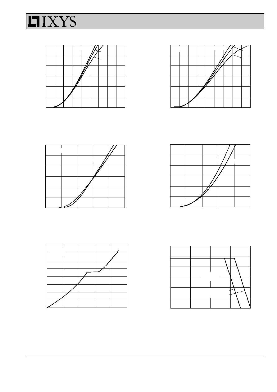
Fig. 1 Typ. Output Characteristics
Fig. 2 Typ. Output Characteristics
Fig. 3 Typ. Transfer Characteristics
Fig. 4 Typ. Characteristics of Reverse
Conduction
Fig. 5 Typ. Gate Charge characteristics
Fig. 6 Reverse Biased Safe Operating Area
RBSOA
IXBF 9N140
IXBF 9N160
© 2000 IXYS All rights reserved
4 - 4
I
C
- Amperes
0
2
4
6
8
10
12
14
16
t
fi
-
n
a
no
s
e
co
nd
s
20
30
40
50
60
70
R
g
- Ohms
0
20
40
60
80
100 120 140 160
t
d(
of
f
)
- na
no
s
e
co
n
d
s
0
50
100
150
200
250
Pulse Width - Seconds
0.0001
0.001
0.01
0.1
1
10
Z
th
JC
-
K/W
0.001
0.01
0.1
1
10
Single Pulse
V
CE
= 960V
V
GE
= 15V
R
G
= 100
W
T
J
= 125∞C
IXBF09
V
CE
= 960V
V
GE
= 15V
I
C
= 5A
T
J
= 125∞C
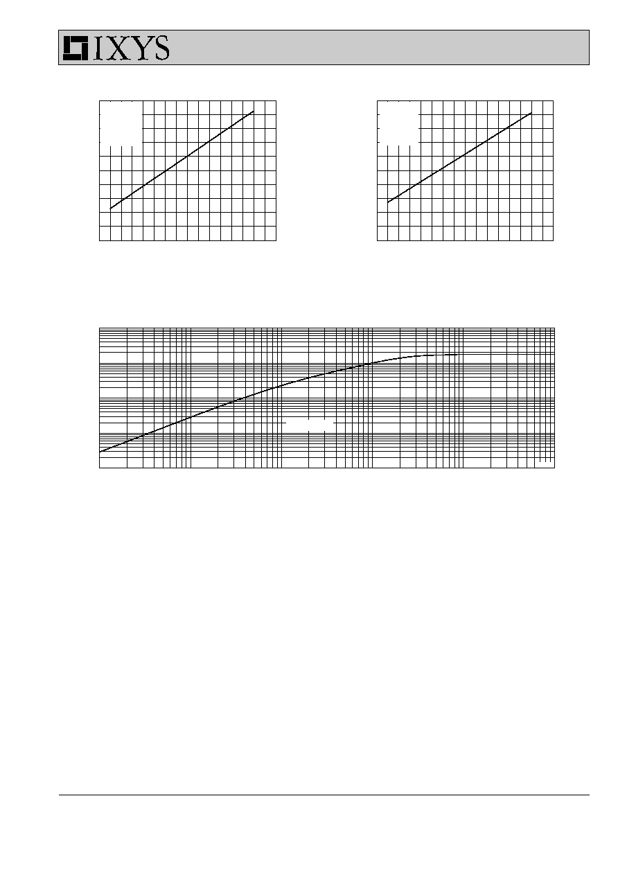
Fig. 7 Typ. Fall Time
Fig. 8 Typ. Turn Off Delay Time
Fig. 9 Typ. Transient Thermal Impedance
IXBF 9N140
IXBF 9N160
