
© 2004 IXYS All rights reserved
1 - 4
MWI 200-06 A8
448
IXYS reserves the right to change limits, test conditions and dimensions.
IXYS reserves the right to change limits, test conditions and dimensions.
Features
∑
NPT IGBT technology
∑
low saturation voltage
∑
low switching losses
∑
switching frequency up to 30 kHz
∑
square RBSOA, no latch up
∑
high short circuit capability
∑
positive temperature coefficient for
easy parallelling
∑
MOS input, voltage controlled
∑
ultra fast free wheeling diodes
∑
solderable pins for PCB mounting
∑
package with copper base plate
Advantages
∑
space savings
∑
reduced protection circuits
∑
package designed for wave soldering
Typical Applications
∑
AC motor control
∑
AC servo and robot drives
∑
power supplies
IGBTs
Symbol
Conditions
Maximum Ratings
V
CES
T
VJ
= 25∞C to 150∞C
600
V
V
GES
± 20
V
I
C25
T
C
= 25∞C
225
A
I
C80
T
C
= 80∞C
155
A
RBSOA
V
GE
=
±15 V; R
G
= 1.5
; T
VJ
= 125∞C
I
CM
= 400
A
Clamped inductive load; L = 100 µH
V
CEK
V
CES
t
SC
V
CE
= V
CES
; V
GE
=
±15 V; R
G
= 1.5
; T
VJ
= 125∞C
10
µs
(SCSOA)
non-repetitive
P
tot
T
C
= 25∞C
675
W
Symbol
Conditions
Characteristic Values
(T
VJ
= 25
∞C, unless otherwise specified)
min.
typ.
max.
V
CE(sat)
I
C
= 200 A; V
GE
= 15 V; T
VJ
= 25∞C
2.0
2.5
V
T
VJ
= 125∞C
2.3
V
V
GE(th)
I
C
= 4 mA; V
GE
= V
CE
4.5
6.5
V
I
CES
V
CE
= V
CES
;
V
GE
= 0 V; T
VJ
= 25∞C
1.8
mA
T
VJ
= 125∞C
1.5
mA
I
GES
V
CE
= 0 V; V
GE
=
± 20 V
400
nA
t
d(on)
180
ns
t
r
50
ns
t
d(off)
300
ns
t
f
40
ns
E
on
4.6
mJ
E
off
6.3
mJ
C
ies
V
CE
= 25 V; V
GE
= 0 V; f = 1 MHz
9.0
nF
Q
Gon
V
CE
= 300 V; V
GE
= 15 V; I
C
= 200 A
670
nC
R
thJC
(per IGBT)
0.18 K/W
Inductive load, T
VJ
= 125∞C
V
CE
= 300 V; I
C
= 200 A
V
GE
= ±15 V; R
G
= 1.5
I
C25
= 225 A
V
CES
= 600 V
V
CE(sat) typ.
= 2.0 V
IGBT Modules
Sixpack
Short Circuit SOA Capability
Square RBSOA
13, 21
14, 20
1
2
3
4
7
8
9
10
11
12
5
6
17
19
15
© 2004 IXYS All rights reserved
2 - 4
MWI 200-06 A8
448
Module
Symbol
Conditions
Maximum Ratings
T
VJ
operating
-40...+125
∞C
T
JM
+150
∞C
T
stg
-40...+125
∞C
V
ISOL
I
ISOL
1 mA; 50/60 Hz
2500
V~
M
d
Mounting torque (M5)
3 - 6
Nm
Symbol
Conditions
Characteristic Values
min.
typ.
max.
R
pin-chip
1.8
m
d
S
Creepage distance on surface
10
mm
d
A
Strike distance in air
10
mm
R
thCH
with heatsink compound
0.01
K/W
Weight
300
g
Diodes
Symbol
Conditions
Maximum Ratings
I
F25
T
C
= 25∞C
260
A
I
F80
T
C
= 80∞C
165
A
Symbol
Conditions
Characteristic Values
min.
typ.
max.
V
F
I
F
= 200 A; V
GE
= 0 V; T
VJ
= 25∞C
1.9
2.1
V
T
VJ
= 125∞C
1.5
V
I
RM
I
F
= 120 A; di
F
/dt = -1000 A/µs; T
VJ
= 125∞C
56
A
t
rr
V
R
= 300 V; V
GE
= 0 V
100
ns
R
thJC
(per diode)
0.3 K/W
Equivalent Circuits for Simulation
Conduction
IGBT (typ. at V
GE
= 15 V; T
J
= 125∞C)
V
0
= 1.1 V; R
0
= 6 m
Free wheeling Diode (typ. at T
J
= 125∞C)
V
0
= 1.1 V; R
0
= 2 m
Thermal Response
IGBT (typ.)
C
th1
= 0.397 J/K; R
th1
= 0.131 K/W
C
th2
= 2.243 J/K; R
th2
= 0.049 K/W
Free wheeling Diode (typ.)
C
th1
= 0.281 J/K; R
th1
= 0.236 K/W
C
th2
= 1.945 J/K; R
th2
= 0.064 K/W
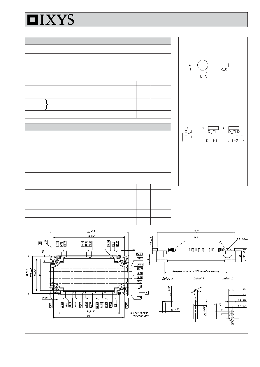
Dimensions in mm (1 mm = 0.0394")
© 2004 IXYS All rights reserved
3 - 4
MWI 200-06 A8
448
0
200
400
600
800
1000
0
60
120
180
0
20
40
60
0
1
2
3
4
0
50
100
150
200
250
300
0
100
200
300
400
500
600
700
0
3
6
9
12
15
0
1
2
3
4
0
50
100
150
200
250
300
V
CE
V
I
C
V
CE
A
I
C
V
Q
G
-di/dt
V
V
GE
I
RM
t
rr
A/
µs
MWI200-06A8
I
RM
t
rr
A
9 V
11 V
A
6
7
8
9
10
11
12
0
100
200
300
400
V
V
GE
A
I
C
0
1
2
0
100
200
300
400
500
600
V
V
F
I
F
A
ns
15 V
T
VJ
= 25∞C
9 V
11 V
13 V
V
GE
= 17 V
T
VJ
= 125∞C
T
VJ
= 25∞C
V
CE
= 20 V
T
VJ
= 125∞C
T
VJ
= 25∞C
13 V
V
GE
= 17 V
15 V
T
VJ
= 125∞C
V
R
= 300 V
I
F
= 120 A
T
VJ
= 125∞C
nC
V
CE
= 300 V
I
C
= 200 A
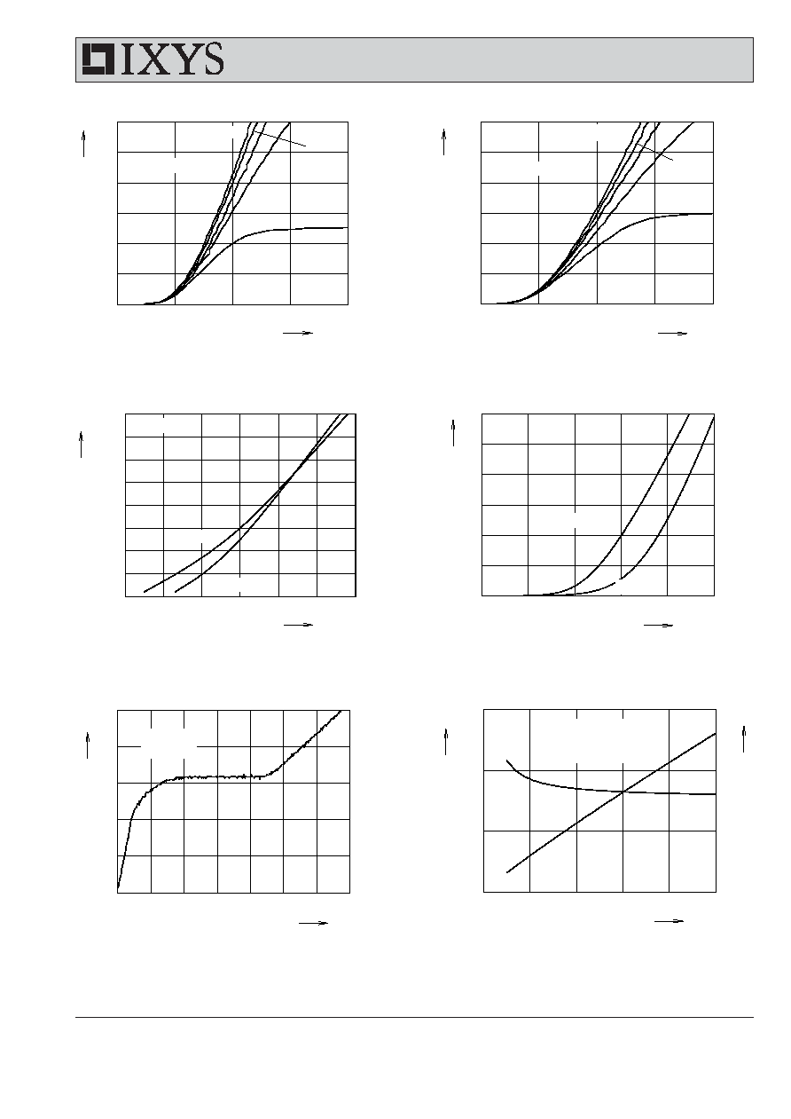
Fig. 1
Typ. output characteristics
Fig. 2
Typ. output characteristics
Fig. 3
Typ. transfer characteristics
Fig. 4
Typ. forward characteristics of
free wheeling diode
Fig. 5
Typ. turn on gate charge
Fig. 6
Typ. turn off characteristics of
free wheeling diode
© 2004 IXYS All rights reserved
4 - 4
MWI 200-06 A8
448
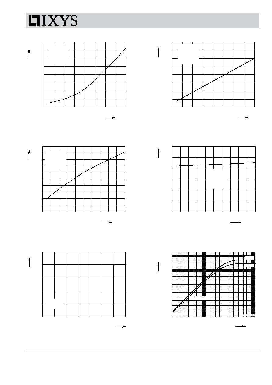
Fig. 11 Reverse biased safe operating area RBSOA
Fig. 12 Typ. transient thermal impedance
Fig. 7
Typ. turn on energy
Fig. 8 Typ. turn off energy
versus collector current
versus collector current
Fig. 9
Typ. turn on energy
Fig.10 Typ. turn off energy
versus gate resistor
versus gate resistor
0
100
200
300
400
0
4
8
12
16
0
100
200
300
400
0
4
8
12
16
0.0001
0.001
0.01
0.1
1
10
0.0001
0.001
0.01
0.1
1
0
4
8
12
16
20
2
4
6
8
0
4
8
12
16
20
0
4
8
12
16
20
0
100
200
300
400
500
600
700
0
100
200
300
400
500
I
C
A
I
C
A
E
off
E
on
R
G
R
G
V
CE
t
s
mJ
E
on
mJ
E
off
I
CM
K/W
Z
thJC
V
A
mJ
mJ
single pulse
diode
IGBT
MWI200-06A8
R
G
= 1.5
T
VJ
= 125∞C
V
CE
= 300 V
V
GE
= ±15 V
R
G
= 1.5
T
VJ
= 125∞C
V
CE
= 300 V
V
GE
= ±15 V
R
G
= 1.5
T
VJ
= 125∞C
V
CE
= 300 V
V
GE
= ±15 V
I
C
= 200
T
VJ
= 125∞C
V
CE
= 300 V
V
GE
= ±15 V
I
C
= 200
T
VJ
= 125∞C