www.clare.com
DS-LIA120-R02.0
1
LIA120
Optically Isolated Linear Error Amplifier
Part #
Description
LIA120S
8 Pin Surface Mount (50/Tube)
LIA120STR
Tape and Reel (1000/Reel)
Applications
Features
Description
Ordering Information
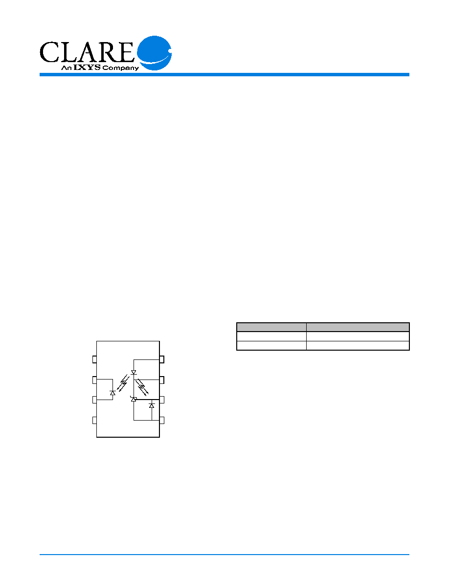
Block Diagram
·
Power supply feedback
·
Telecom central office supply
·
Telecom bricks
·
Modem transformer replacement
·
Digital telephone isolation
·
Optocoupler, precision reference and error
amplifier in single package
·
Low voltage operation 2.7V
·
1.240V ± 2.5% reference
·
CTR Matching 15%
·
>70dB THD
·
70dB CMRR
·
3,750V
rms
isolation
·
UL approval pending
The LIA120 Optically Isolated Reference Amplifier
combines Clare's linear optical coupler technology
with an industry standard 431 type precision
programmable shunt regulator to provide very
linear high gain with excellent temperature stability
for a total gain error of less than 2dB. By using
optical feedback, the LIA120 essentially eliminates
temperature and gain variations due to current
transfer ratio (CTR) changes in optocouplers while
increasing the bandwidth up to 10X and easing
engineering design constraints.
The LIA120 is very well suited for high gain feedback
amplifiers that require excellent linearity and low
temperature variation such as isolated power
supply feedback stages, modem audio transformer
replacement, isolated industrial control signals, and
sensor feedback.
By using the LIA120, system designers can save
precious board space and reduce component count.
Available in an 8 pin surface mount package.
1
2
3
4
5
6
7
8 LED (Input)
FB
COMP
GND
NC
K
A
NC
www.clare.com
2
LIA120
Rev. 2.0
Absolute Maximum Ratings are stress ratings. Stresses in
excess of these ratings can cause permanent damage to
the device. Functional operation of the device at conditions
beyond those indicated in the operational sections of this
data sheet is not implied.
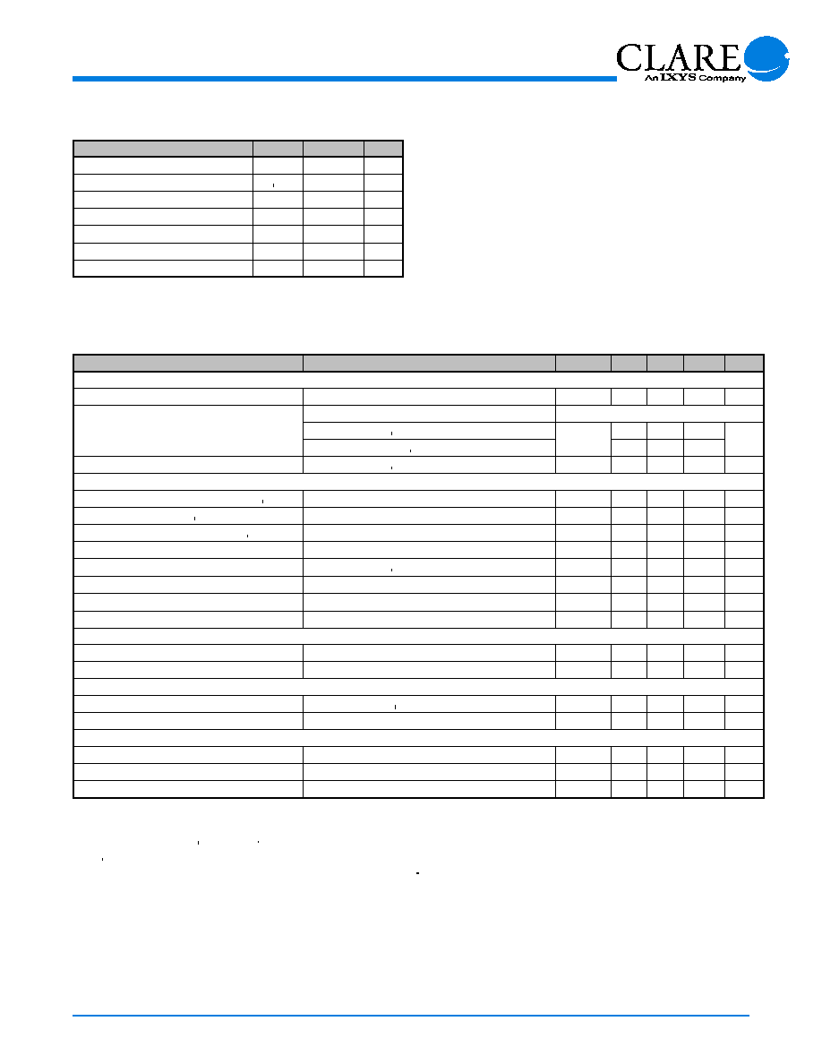
Parameter
Conditions
Symbol Min
Typ
Max Units
Input Characteristics @ 25°C
LED forward voltage
I
LED
= 5 mA, V
COMP
= V
FB
(Fig.1)
V
F
0.8
1.2
1.4
V
Reference voltage
I
LED
= 10 mA, V
COMP
= V
FB
(Fig.1)
T
A
T
T = -40 to +85°C
V
REF
1.210
-
1.265
V
T
A
T
T = 25°C
1.228 1.24
1.252
Deviation of V
REF
over temperature -
See Note 1
T
A
T
T = -40 to +85°C
V
REF (DEV)
REF (DEV)
-
32
-
mV
Transfer Characteristics @ 25°C
Current Transfer Ratio in Feedback (I
REF
/I
REF
REF LED
)
I
LED
= 5mA, V
REF
= 0.5V
(Fig.2)
K
1
1.0
2
3.0
%
Current transfer ratio (I
KA
/I
KA
KA LED
)
I
LED
= 5 mA, V
COMP
= V
FB
, V
KA
= 5 V
(Fig. 4)
K
2
1.0
2
3.0
%
Current Transfer Ratio Matching (I
KA
/I
KA
KA REF
)
I
LED
= 5mA, V
KA
= 5.0V
K
3
85
100
115
%
Feedback input current
I
LED
= 10 mA, R1 = 10 k
(Fig.2)
I
REF
-
226
-
µA
Deviation of I
REF
over temperature -
See Note 1
T
A
T
T = -40 to +85°C
I
REF (DEV)
REF (DEV)
-
110
-
µA
Minimum drive current
V
COMP
= V
FB
(Fig.1)
I
LED (MIN)
LED (MIN)
1
-
-
mA
Off-state error amplifier current
V
IN
= 6 V, V
FB
= 0
(Fig.3)
I
OFF
-
0.001
0.1
µA
Error amplifier output impedance -
See Note 2
I
LED
= 0.1 mA to 15 mA, V
COMP
= V
FB
, f<1 kHz
(Fig.1)
IZ
OUT
I
-
0.21
-
Ohm
Output Characteristics @ 25°C
Cathode dark current
V
IN
= Open, V
KA
= 10V
(Fig. 3)
I
KAO
-
0.3
100
nA
Cathode-Anode voltage breakdown
I
KA
= 1µA
BV
KA
20
-
-
V
Isolation Characteristics @ 25°C
Withstand insulation voltage
RH 50%, T
A
50%, T
50%, T = 25°C, t = 1 min
(Note 3)
V
ISO
3750
-
-
V
rms
Resistance (input to output)
V
I-O
= 500 V
DC
(Note 3)
R
I-O
-
10
12
-
AC Characteristics @ 25°C
Bandwidth (LED) -
See Note 4
B
W
-
100
-
kHz
Common mode rejection ratio -
See Note 5
I
LED
= 1.0 mA, R
L
= 100 k, f = 100 Hz
(Fig. 5)
CMRR
-
70
-
dB
Linearity
I
LED
= 5 mA, 100 mV
PP
THD
-
70
-
dB
1. The deviation parameters V
REF(DEV)
and I
REF(DEV)
are defined as the differences between the maximum and minimum values obtained over the rated temperature range. The average full-range temperature
coefficient of the reference input voltage, V
REF
, is defined as:
|V
REF
| (ppm/°C) = {V
REF (DEV)
/V
REF
(T
A
(T
(T 25°C)} X 10
6
/ T
A
T
T
where T
A
T
T is the rated operating free-air temperature range of the device.
2. The dynamic impedance is defined as |Z
OUT
| = V
COMP
/I
LED
, for the application circuit in Figure 6, |Zout| = K
1
R
1
3. Device is considered as a two terminal device: Pins 1, 2, 3 and 4 are shorted together and Pins 5, 6, 7 and 8 are shorted together.
4. See compensation section for calculating bandwidth of LIA120.
5. Common mode transient immunity at output high is the maximum tolerable (positive) dVcm/dt on the leading edge of the common mode impulse signal, Vcm, to assure that the output will remain high.
Common mode transient immunity at output low is the maximum tolerable (negative) dVcm/dt on the trailing edge of the common pulse signal,Vcm, to assure that the output will remain low.
Electrical Characteristics:
Parameter
Symbol Ratings Units
Photodiode Cathode-Anode Voltage
V
KAO
20
V
Photodiode Anode-Cathode Voltage
V
AKO
V
V
0.5
V
Input Voltage
V
LED
9
V
Input DC Current
I
LED
20
mA
Total Power Dissipation
(note 1)
P
D
145
mW
Operating Temperature
T
-40 to +85
°C
Storage Temperature
T
-40 to +125
°C
Absolute Maximum Ratings (@ 25° C)
1
Derate linearly from 25°C at a rate of 2.42 mW/ °C.
, for the application circuit in Figure 6, |Zout| = K
, for the application circuit in Figure 6, |Zout| = K

www.clare.com
4
LIA120
Rev. 2.0
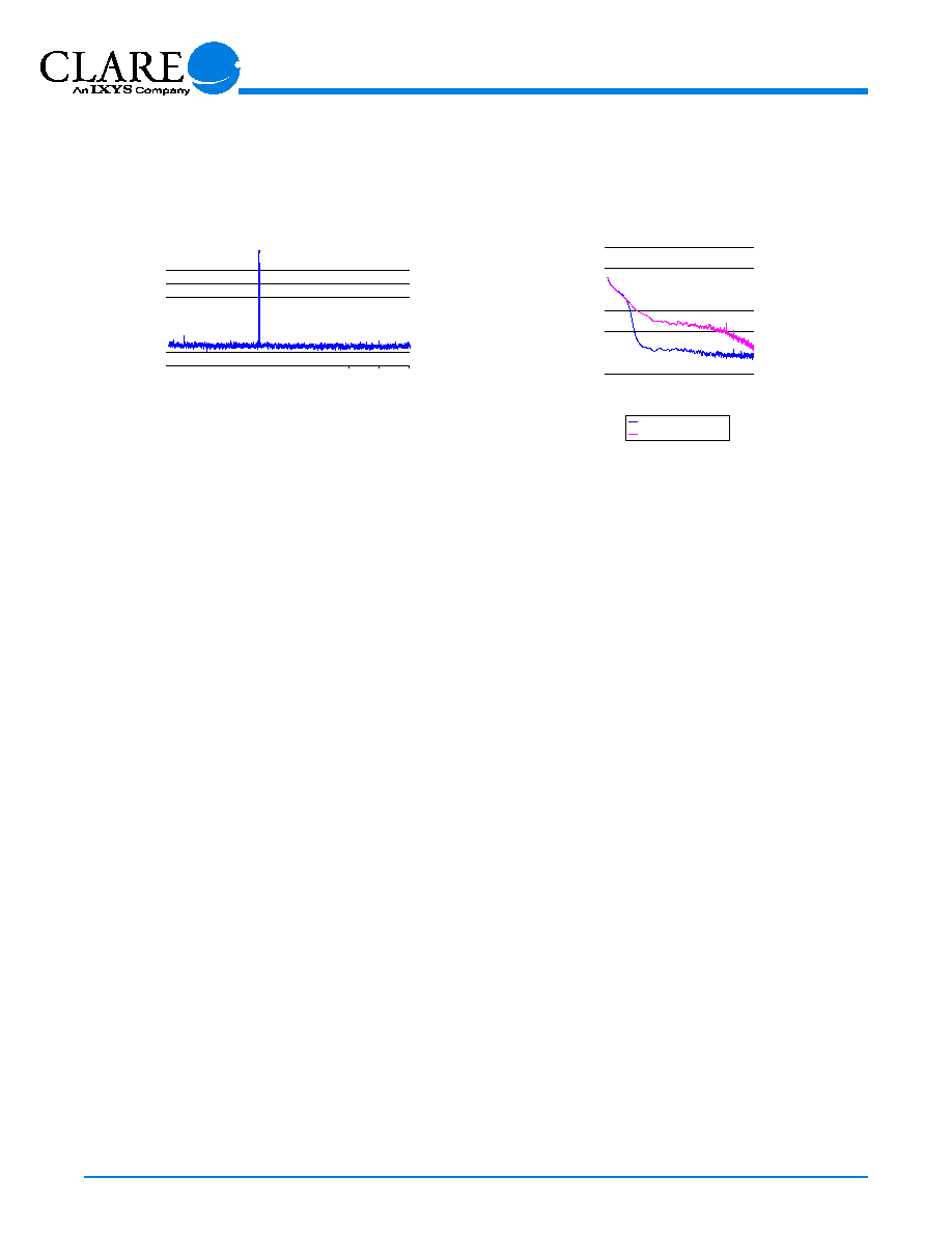
PERFORMANCE DATA*
*The Performance data shown in the graphs above is typical of device performance. For guaranteed parameters not indicated in the written specifi cations, please contact our
application department.
LIA120
LED Current vs. Cathode Voltage
V
COMP
- Cathode Voltage (V)
I
LED
- Supply Current (mA)
-1.0
15
10
5
0
-5
-10
-15
-0.5
0.0
0.5
1.0
1.5
LIA120
LED Current vs. Cathode Voltage
V
COMP
- Cathode Voltage (V)
I
LED
- Supply Current (µA)
-1.0
150
120
90
60
30
0
-30
-60
-90
-120
-150
-0.5
0.0
0.5
1.0
1.5
LIA120
Reference Voltage vs.
Ambient Temperature
V
REF
- Reference V
oltage (V
)
-40
1.30
1.37
1.24
1.21
1.18
-20
0
20
40
60
80
I
LED
= 10mA
LIA120
Reference Current vs.
Ambient Temperature
I
REF
- Reference Current (µA)
-40
350
300
250
200
150
100
50
-20
0
20
40
60
80
100
I
LED
= 10mA
R
1
= 10 k
LIA120
Off Current vs. Ambient Temperature
I
(OFF)
- Off Current (nA)
-40
2.5
2.0
1.5
1.0
0.5
0
-20
0
20
40
60
80
100
V
IN
= 10V
V
FB
= 0
LIA120
LED Forward Current vs. Forward Voltage
I
LED
- Forward Current (mA)
V
F
- Forward-Voltage (V)
20
15
10
5
0
1.0
1.1
1.2
1.3
1.4
1.5
85ºC
55
º
C
25
º
C -5ºC
LIA120
Dark Current vs. Temperature
I
KAO
- Dark Current (nA)
V
KA
= 10V
-40
50
40
30
20
10
0
-10
-20
0
20
40
60
80
100
LIA120
Cathode Current vs. Ambient Temperature
I
K
- Cathode Current (µA)
V
KA
= 5V
I
LED
= 20mA
I
LED
= 10mA
I
LED
= 5mA
I
LED
= 1mA
-40
1400
1200
1000
800
600
400
200
0
-20
0
20
40
60
80
100
LIA120
Current Transfer Ratio vs LED Current
(I
KA
/I
F
) - Current T
ransfer Ratio (%)
I
LED
- Forward Current (mA)
V
KA
= 5V
0
3.5
3.0
2.5
2.0
1.5
1.0
0.5
0
10
20
30
40
50
LIA120
Cathode Current vs. Photodiode Voltage
I
K
- Cathode Current (µA)
V
KA
(V)
0
500
450
400
350
300
250
200
150
100
50
0
1
2
3
4
5
6
7
8
9
10
I
LED
= 20mA
I
LED
= 10mA
I
LED
= 5mA
I
LED
= 1mA
LIA120
Bandwidth vs. Temperature for
High Frequency Applications
Frequency (kHz)
0
50
40
30
20
10
0
10
20
30
40
50
60
70
80
90
LIA120
Voltage Gain vs. Frequency
V
oltage Gain, A(V
o
/V
in
) dB
Frenquency kHz
10
60
40
20
0
100
1000