© 2003 IXYS All rights reserved
1 - 4
Advanced Technical Information
Converter - Brake - Inverter Module
(CBI3)
Input Rectifier D11 - D16
Symbol
Conditions
Maximum Ratings
V
RRM
1600
V
I
FAV
T
C
= 80°C; sine 180°
65
A
I
DAVM
T
C
= 80°C; rectangular; d = 1/3; bridge
180
A
I
FSM
T
VJ
= 25°C; t = 10 ms; sine 50 Hz
850
A
P
tot
T
C
= 25°C
170
W
Symbol
Conditions
Characteristic Values
(T
VJ
= 25
°
C, unless otherwise specified)
min.
typ.
max.
V
F
I
F
= 100 A; T
VJ
= 25°C
1.3
1.5
V
T
VJ
= 125°C
1.3
V
I
R
V
R
= V
RRM
;
T
VJ
= 25°C
0.05
mA
T
VJ
= 125°C
1
mA
R
thJC
(per diode)
0.73 K/W
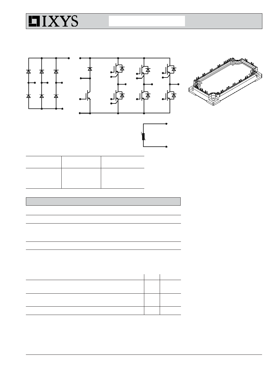
Three Phase
Brake Chopper
Three Phase
Rectifier
Inverter
V
RRM
= 1600 V
V
CES
= 600 V
V
CES
= 600 V
I
FAVM
= 90 A
I
C25
= 50 A
I
C25
= 125 A
I
FSM
= 850 A
V
CE(sat)
= 1.9 V
V
CE(sat)
= 1.9 V
MUBW 100-06 A8
IXYS reserves the right to change limits, test conditions and dimensions.
Application: AC motor drives with
Input from single or three phase grid
Three phase synchronous or
asynchronous motor
electric braking operation
Features
High level of integration - only one power
semiconductor module required for the
whole drive
NPT IGBT technology with low
saturation voltage, low switching
losses, high RBSOA and short circuit
ruggedness
Epitaxial free wheeling diodes with
Hiperfast and soft reverse recovery
Industry standard package with insulated
copper base plate and soldering pins for
PCB mounting
Temperature sense included
NTC
D11
D13
D15
D12
D14
D16
1
2
3
D7
T7
T1
D1
T3
D3
T2
T4
T6
T5
D4
D2
D6
D5
21
22
7
6
4
5
16
15
18
17
20
19
11
10
23
24
14
8
9
12
13
Revision A 07.03.2001
3
1
2
© 2003 IXYS All rights reserved
2 - 4
B4
MUBW 100-06 A8
Output Inverter T1 - T6
Symbol
Conditions
Maximum Ratings
V
CES
T
VJ
= 25°C to 150°C
600
V
V
GES
Continuous
±
20
V
I
C25
T
C
= 25°C
125
A
I
C80
T
C
= 80°C
85
A
RBSOA
V
GE
=
±
15 V; R
G
= 2.2
; T
VJ
= 125°C
I
CM
= 200
A
Clamped inductive load; L = 100 µH
V
CEK
V
CES
t
SC
V
CE
= V
CES
; V
GE
=
±
15 V; R
G
= 2.2
; T
VJ
= 125°C
10
µs
(SCSOA)
non-repetitive
P
tot
T
C
= 25°C
410
W
Symbol
Conditions
Characteristic Values
(T
VJ
= 25
°
C, unless otherwise specified)
min.
typ.
max.
V
CE(sat)
I
C
= 100 A; V
GE
= 15 V; T
VJ
= 25°C
1.9
2.5
V
T
VJ
= 125°C
2.2
V
V
GE(th)
I
C
= 1.5 mA; V
GE
= V
CE
4.5
6.5
V
I
CES
V
CE
= V
CES
;
V
GE
= 0 V; T
VJ
= 25°C
1.4
mA
T
VJ
= 125°C
1.5
mA
I
GES
V
CE
= 0 V; V
GE
=
±
20 V
400
nA
t
d(on)
25
ns
t
r
11
ns
t
d(off)
150
ns
t
f
30
ns
E
on
1.0
mJ
E
off
2.9
mJ
C
ies
V
CE
= 25 V; V
GE
= 0 V; f = 1 MHz
4.3
nF
Q
Gon
V
CE
= 300V; V
GE
= 15 V; I
C
= 100 A
tbd
nC
R
thJC
(per IGBT)
0.3 K/W
Inductive load, T
VJ
= 125°C
V
CE
= 300 V; I
C
= 100 A
V
GE
= ±15 V; R
G
= 2.2
Output Inverter D1 - D6
Symbol
Conditions
Maximum Ratings
I
F25
T
C
= 25°C
140
A
I
F80
T
C
= 80°C
85
A
Symbol
Conditions
Characteristic Values
min.
typ.
max.
V
F
I
F
= 60 A; V
GE
= 0 V; T
VJ
= 25°C
1.8
2.1
V
T
VJ
= 125°C
1.3
V
I
RM
I
F
= 60 A; di
F
/dt = -500 A/µs; T
VJ
= 125°C
28
A
t
rr
V
R
= 300 V; V
GE
= 0 V
100
ns
R
thJC
(per diode)
0.61 K/W
3
1
2
© 2003 IXYS All rights reserved
3 - 4
MUBW 100-06 A8
Brake Chopper T7
Symbol
Conditions
Maximum Ratings
V
CES
T
VJ
= 25°C to 150°C
600
V
V
GES
Continuous
±
20
V
I
C25
T
C
= 25°C
75
A
I
C80
T
C
= 80°C
50
A
RBSOA
V
GE
=
±
15 V; R
G
= 22
; T
VJ
= 125°C
I
CM
= 100
A
Clamped inductive load; L = 100 µH
V
CEK
V
CES
t
SC
V
CE
= V
CES
; V
GE
=
±
15 V; R
G
= 22
; T
VJ
= 125°C
10
µs
(SCSOA)
non-repetitive
P
tot
T
C
= 25°C
225
W
Symbol
Conditions
Characteristic Values
(T
VJ
= 25
°
C, unless otherwise specified)
min.
typ.
max.
V
CE(sat)
I
C
= 50 A; V
GE
= 15 V; T
VJ
= 25°C
1.9
2.3
V
T
VJ
= 125°C
2.1
V
V
GE(th)
I
C
= 1 mA; V
GE
= V
CE
4.5
6.5
V
I
CES
V
CE
= V
CES
;
V
GE
= 0 V; T
VJ
= 25°C
0.5
mA
T
VJ
= 125°C
0.5
mA
I
GES
V
CE
= 0 V; V
GE
=
±
20 V
200
nA
t
d(on)
50
ns
t
r
55
ns
t
d(off)
300
ns
t
f
30
ns
E
on
2.3
mJ
E
off
1.7
mJ
C
ies
V
CE
= 25 V; V
GE
= 0 V; f = 1 MH z
2.8
nF
Q
Gon
V
CE
= 300 V; V
GE
= 15 V; I
C
= 50 A
120
nC
R
thJC
0.55 K/W
Brake Chopper D7
Symbol
Conditions
Maximum Ratings
V
RRM
T
VJ
= 25°C to 150°C
600
V
I
F25
T
C
= 25°C
35
A
I
F80
T
C
= 80°C
24
A
Symbol
Conditions
Characteristic Values
min.
typ.
max.
V
F
I
F
= 50 A; T
VJ
= 25°C
2.5
2.7
V
T
VJ
= 125°C
2.2
V
I
R
V
R
= V
RRM
;
T
VJ
= 25°C
0.1
mA
T
VJ
= 125°C
0.1
mA
I
RM
I
F
= 15 A; di
F
/dt = -400 A/µs; T
VJ
= 125°C
13
A
t
rr
V
R
= 300 V
90
ns
R
thJC
2.1 K/W
Inductive load, T
VJ
= 125°C
V
CE
= 300 V; I
C
= 50 A
V
GE
= ±15 V; R
G
= 22
3
1
2
© 2003 IXYS All rights reserved
4 - 4
B4
MUBW 100-06 A8
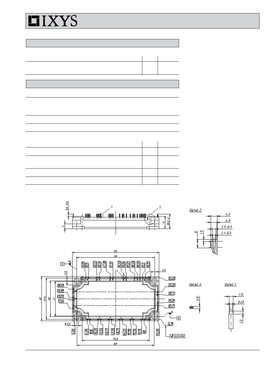
Dimensions in mm (1 mm = 0.0394")
3
1
2
Temperature Sensor NTC
Symbol
Conditions
Characteristic Values
min.
typ.
max.
R
25
T = 25°C
4.75
5.0
5.25
k
B
25/50
3375
K
Module
Symbol
Conditions
Maximum Ratings
T
VJ
operating
-40...+125
°
C
T
JM
+150
°
C
T
stg
-40...+125
°
C
V
ISOL
I
ISOL
1 mA; 50/60 Hz
2500
V~
M
d
Mounting torque (M5)
3 - 6
Nm
Symbol
Conditions
Characteristic Values
min.
typ.
max.
R
pin-chip
5
m
d
S
Creepage distance on surface
6
mm
d
A
Strike distance in air
6
mm
R
thCH
with heatsink compound
0.01
K/W
Weight
300
g