© 2000 IXYS All rights reserved
1 - 3
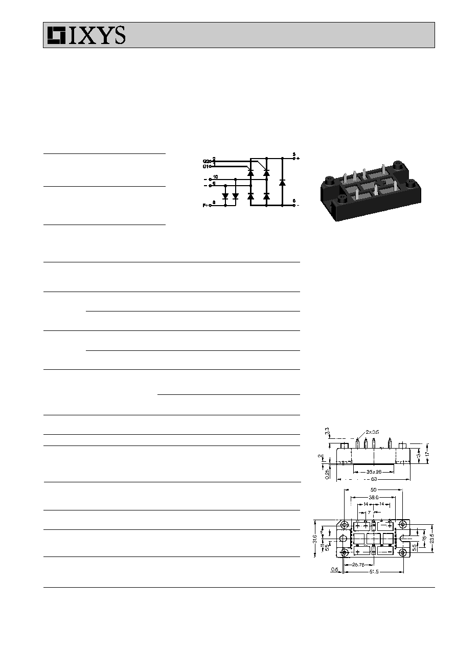
Symbol
Test Conditions
Maximum Ratings
I
dAV
T
H
= 85
∞
C, module
16
A
I
dAVM
x
module
21
A
I
FRMS
, I
TRMS
per leg
15
A
I
FSM
, I
TSM
T
VJ
= 45
∞
C;
t = 10 ms (50 Hz), sine
150
A
V
R
= 0 V
t = 8.3 ms (60 Hz), sine
170
A
T
VJ
= T
VJM
t = 10 ms (50 Hz), sine
130
A
V
R
= 0 V
t = 8.3 ms (60 Hz), sine
140
A
I
2
t
T
VJ
= 45
∞
C
t = 10 ms (50 Hz), sine
110
A
2
s
V
R
= 0 V
t = 8.3 ms (60 Hz), sine
120
A
2
s
T
VJ
= T
VJM
t = 10 ms (50 Hz), sine
85
A
2
s
V
R
= 0 V
t = 8.3 ms (60 Hz), sine
80
A
2
s
(di/dt)
cr
T
VJ
= 125
∞
C
repetitive, I
T
= 50 A
150
A/
m
s
f = 50 Hz, t
P
= 200
m
s
V
D
= 2/3 V
DRM
I
G
= 0.3 A,
non repetitive, I
T
= 0.5 I
dAV
500
A/
m
s
di
G
/dt = 0.3 A/
m
s
(dv/dt)
cr
T
VJ
= T
VJM
; V
DR
= 2/3 V
DRM
1000
V/
m
s
R
GK
=
•
; method 1 (linear voltage rise)
V
RGM
10
V
P
GM
T
VJ
= T
VJM
t
p
=
30
m
s
£
10
W
I
T
= 0.5 I
dAVM
t
p
= 500
m
s
£
5
W
t
p
=
10 ms
£
1
W
P
GAVM
0.5
W
T
VJ
-40...+125
∞
C
T
VJM
125
∞
C
T
stg
-40...+125
∞
C
V
ISOL
50/60 Hz, RMS
t = 1 min
3000
V~
I
ISOL
£
1 mA
t = 1 s
3600
V~
d
S
Creep distance on surface
12.7
mm
d
A
Strike distance in air
9.4
mm
a
Max. allowable acceleration
50
m/s
2
M
d
Mounting torque
(M5)
2-2.5
Nm
(10-32 UNF)
18-22
lb.in.
Weight
35
g
V
RSM
V
RRM
Type
V
DSM
V
DRM
V
V
900
800
VHFD 16-08io1
1300
1200
VHFD 16-12io1
1500
1400
VHFD 16-14io1
1700
1600
VHFD 16-16io1
Bridge and Freewheeling Diode
Features
q
Package with DCB ceramic base plate
q
Isolation voltage 3600 V~
q
Planar passivated chips
q
Blocking voltage up to 1600 V
q
Low forward voltage drop
q
Leads suitable for PC board soldering
q
UL registered E 72873
Applications
q
Supply for DC power equipment
q
DC motor control
Advantages
q
Easy to mount with two screws
q
Space and weight savings
q
Improved temperature and power
cycling
Dimensions in mm (1 mm = 0.0394")
V
RRM
= 800-1600 V
I
dAVM
= 21 A
VHFD 16
Half Controlled
Single Phase Rectifier Bridge
Including Freewheeling Diode and Field Diodes
1
3
5
2
6
8
10

© 2000 IXYS All rights reserved
2 - 3
VHFD 16
Symbol
Test Conditions
Characteristic Values
I
R
, I
D
V
R
= V
RRM
; V
D
= V
DRM
T
VJ
= T
VJM
£
5
mA
T
VJ
= 25
∞
C
£
0.3
mA
V
T
, V
F
I
T
, I
F
= 45 A; T
VJ
= 25
∞
C
£
2.55
V
V
T0
For power-loss calculations only (T
VJ
= 125∞C)
1.0
V
r
T
40
m
W
V
GT
V
D
= 6 V;
T
VJ
= 25
∞
C
£
1.0
V
T
VJ
= -40
∞
C
£
1.2
V
I
GT
V
D
= 6 V;
T
VJ
= 25
∞
C
£
65
mA
T
VJ
= -40
∞
C
£
80
mA
T
VJ
= 125
∞
C
£
50
mA
V
GD
T
VJ
= T
VJM
;
V
D
= 2/3 V
DRM
£
0.2
V
I
GD
T
VJ
= T
VJM
;
V
D
= 2/3 V
DRM
£
5
mA
I
L
I
G
= 0.3 A; t
G
= 30
m
s;
T
VJ
= 25
∞
C
£
150
mA
di
G
/dt = 0.3 A/
m
s;
T
VJ
= -40
∞
C
£
200
mA
T
VJ
= 125
∞
C
£
100
mA
I
H
T
VJ
= 25
∞
C; V
D
= 6 V; R
GK
=
•
£
100
mA
t
gd
T
VJ
= 25
∞
C; V
D
= 0.5V
DRM
£
2
m
s
I
G
= 0.3 A; di
G
/dt = 0.3 A/
m
s
t
q
T
VJ
= 125
∞
C, I
T
= 15 A, t
P
= 300
m
s, V
R
= 100 V
typ.
150
m
s
Q
r
di/dt = -10 A/
m
s, dv/dt = 20 V/
m
s, V
D
= 2/3 V
DRM
75
m
C
R
thJC
per thyristor (diode); DC current
2.4
K/W
per module
0.6
K/W
R
thJH
per thyristor (diode); DC current
3.0
K/W
per module
0.75
K/W
Symbol
Test Conditions
Maximum Ratings
I
FAV
T
H
= 85
∞
C, per Diode
4
A
I
FAVM
per diode
4
A
I
FRMS
per diode
6
A
I
FSM
T
VJ
= 45
∞
C;
t = 10 ms (50 Hz), sine
100
A
V
R
= 0 V
t = 8.3 ms (60 Hz), sine
110
A
T
VJ
= T
VJM
t = 10 ms (50 Hz), sine
85
A
V
R
= 0 V
t = 8.3 ms (60 Hz), sine
94
A
I
2
t
T
VJ
= 45
∞
C
t = 10 ms (50 Hz), sine
50
A
2
s
V
R
= 0 V
t = 8.3 ms (60 Hz), sine
50
A
2
s
T
VJ
= T
VJM
t = 10 ms (50 Hz), sine
36
A
2
s
V
R
= 0 V
t = 8.3 ms (60 Hz), sine
37
A
2
s
I
R
V
R
= V
RRM
T
VJ
= T
VJM
1
mA
T
VJ
= 25
∞
C
0.15
mA
V
F
I
F
= 21 A; T
VJ
= 25
∞
C
1.83
V
V
T0
For power-loss calculations only (T
VJ
= 125∞C)
0.9
V
r
T
50
m
W
R
thJC
per diode; DC current
4.4
K/W
R
thJH
per diode; DC current
5.2
K/W
Field Diodes
Data according to IEC 60747 and refer to a single thyristor/diode unless otherwise stated.
x
for resistive load
IXYS reserves the right to change limits, test conditions and dimensions.
Fig. 1 Gate trigger range
Fig. 2 Gate controlled delay time t
gd
1
10
100
1000
0.1
1
10
I
G
V
G
mA
1: I
GT
, T
VJ
= 125∞C
2: I
GT
, T
VJ
= 25∞C
3: I
GT
, T
VJ
= -40∞C
V
4: P
GAV
= 0.5 W
5: P
GM
= 1 W
6: P
GM
= 10 W
I
GD
, T
VJ
= 125∞C
4
2
1
5
6
10
100
1000
1
10
100
1000
µ
s
t
gd
T
VJ
= 25∞C
typ.
Limit
mA
I
G
3
750

© 2000 IXYS All rights reserved
3 - 3
VHFD 16
2
3
4
5 6 7 8 9
1
10
10
1
10
2
10
3
0.001
0.01
0.1
1
0
20
40
60
80
100
120
0
1
2
3
4
0
10
20
30
40
50
60
70
0
5
10
15
20
25
0
10
20
30
40
50
60
70
80
90
0
20
40
60
80
100 120 140
0
0.001
0.01
0.1
1
10
0.0
0.5
1.0
1.5
2.0
2.5
3.0
3.5
I
2
t
I
FSM
I
F
A
V
F
t
s
t
ms
P
tot
W
I
d(AV)M
A
T
amb
t
s
Z
thJH
K/W
A
2
s
0
20
40
60
80 100 120
0
5
10
15
20
25
I
d(AV)M
T
H
A
V
A
∞C
∞C
T
VJ
=125∞C
T
VJ
= 25∞C
T
VJ
= 45∞C
typ.
max.
50Hz, 80% V
RRM
T
VJ
= 125∞C
T
VJ
= 45∞C
T
VJ
= 125∞C
V
R
= 0 V
Fig. 3 Forward current versus voltage
drop per diode
Fig. 4 Surge overload current
Fig. 5 I
2
t versus time per diode
Fig. 6 Power dissipation versus direct output current and ambient temperature
Fig. 7 Max. forward current versus
heatsink temperature
Fig. 8 Transient thermal impedance junction to heatsink
Constants for Z
thJH
calculation:
i
R
thi
(K/W)
t
i
(s)
1
0.01
0.008
2
0.4
0.05
3
1.69
0.06
4
0.9
0.25
R
thHA
:
0.5 K/W
1.0 K/W
1.5 K/W
2.0 K/W
3.0 K/W
4.0 K/W
6.0 K/W