© 2003 IXYS All rights reserved
1 - 4
IXYS reserves the right to change limits, test conditions and dimensions.
VDI
75-12P1 VII
75-12P1
VID
75-12P1 VIO
75-12P1
303
B3
I
C25
= 92 A
V
CES
= 1200 V
V
CE(sat) typ.
= 2.7 V
IGBTs
Symbol
Conditions
Maximum Ratings
V
CES
T
VJ
= 25∞C to 150∞C
1200
V
V
GES
± 20
V
I
C25
T
C
= 25∞C
92
A
I
C80
T
C
= 80∞C
62
A
I
CM
V
GE
= ±15 V; R
G
= 22
; T
VJ
= 125∞C
100
A
V
CEK
RBSOA, Clamped inductive load; L = 100 µH
V
CES
t
SC
V
CE
= V
CES
; V
GE
= ±15 V; R
G
= 22
; T
VJ
= 125∞C
10
µs
(SCSOA)
non-repetitive
P
tot
T
C
= 25∞C
379
W
Symbol
Conditions
Characteristic Values
(T
VJ
= 25
∞
C, unless otherwise specified)
min.
typ.
max.
V
CE(sat)
I
C
= 75 A; V
GE
= 15 V; T
VJ
= 25∞C
2.7
3.2
V
T
VJ
= 125∞C
3.0
V
V
GE(th)
I
C
= 2 mA; V
GE
= V
CE
4.5
6.5
V
I
CES
V
CE
= V
CES
;
V
GE
= 0 V;
T
VJ
= 25∞C
3.7
mA
T
VJ
= 125∞C
12.5
mA
I
GES
V
CE
= 0 V; V
GE
=
±
20 V
200
nA
t
d(on)
100
ns
t
r
70
ns
t
d(off)
500
ns
t
f
70
ns
E
on
9.1
mJ
E
off
6.7
mJ
C
ies
V
CE
= 25 V; V
GE
= 0 V; f = 1 MHz
3.3
nF
R
thJC
(per IGBT)
0.33 K/W
R
thJH
with heatsink compound (0.42 K/m.K; 50 µm)
0.66
K/W
Inductive load, T
VJ
= 125∞C
V
CE
= 600 V; I
C
= 60 A
V
GE
= 15/0 V; R
G
= 22
IGBT Modules
in ECO-PAC 2
Short Circuit SOA Capability
Square RBSOA
Preliminary data sheet
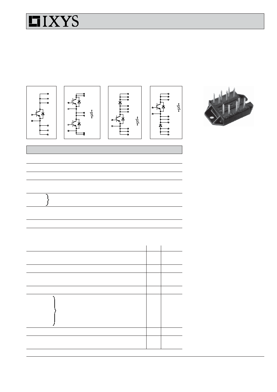
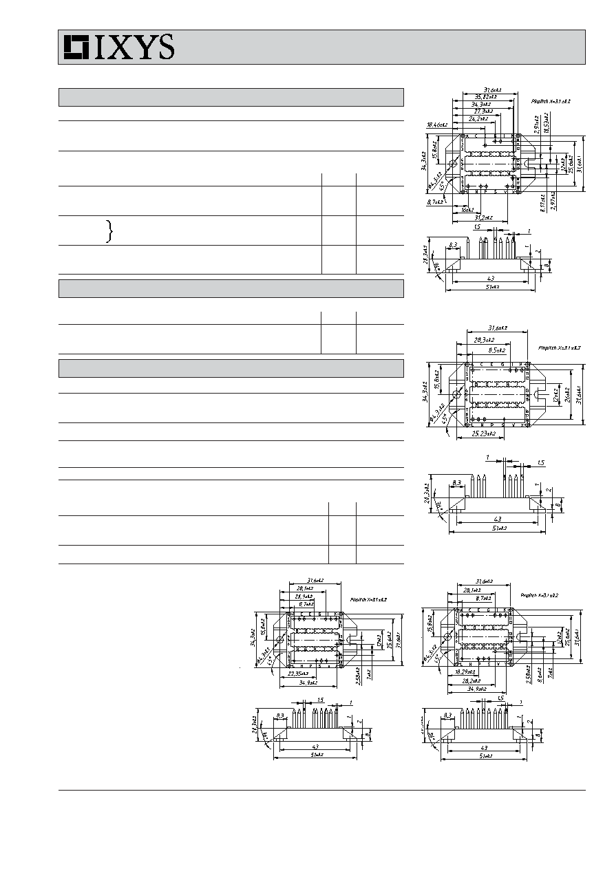
Pin arangement see outlines
VII
OP9
GH10
VX18
L9
E2
K10
X16
X13
X15
NTC
VIO
IJK
LMN
A
VDI
X15
X16
NTC
AC1
PS18
IK10
L9
T16
VID
IK10
SV18
AC1
L9
F1
X15
X16
NTC
Features
∑ NPT IGBT's
- positive temperature coefficient of
saturation voltage
- fast switching
∑ FRED diodes
- fast reverse recovery
- low forward voltage
∑ Industry Standard Package
- solderable pins for PCB mounting
- isolated DCB ceramic base plate
Advantages
∑ space and weight savings
∑ reduced protection circuits
∑ leads with expansion bend for stress relief
Typical Applications
∑ AC and DC motor control
∑ AC servo and robot drives
∑ power supplies
∑ welding inverters
S
© 2003 IXYS All rights reserved
2 - 4
IXYS reserves the right to change limits, test conditions and dimensions.
VDI
75-12P1 VII
75-12P1
VID
75-12P1 VIO
75-12P1
303
B3
Reverse diodes (FRED)
Symbol
Conditions
Maximum Ratings
I
F25
T
C
= 25∞C
103
A
I
F80
T
C
= 80∞C
65
A
Symbol
Conditions
Characteristic Values
min.
typ.
max.
V
F
I
F
= 60 A; T
VJ
= 25∞C
2.28
2.6
V
T
VJ
= 125∞C
1.67
V
I
RM
I
F
= 60 A; di
F
/dt = 500 A/µs; T
VJ
= 125∞C
41
A
t
rr
V
R
= 600 V; V
GE
= 0 V
200
ns
R
thJC
0.66 K/W
R
thJH
with heatsink compound (0.42 K/m.K; 50 µm)
1.32
K/W
Module
Symbol
Conditions
Maximum Ratings
T
VJ
-40...+150
∞
C
T
stg
-40...+150
∞
C
V
ISOL
I
ISOL
1 mA; 50/60 Hz
3000
V~
M
d
mounting torque (M4)
1.5 - 2.0
Nm
14 - 18
lb.in.
a
Max. allowable acceleration
50
m/s
2
Symbol
Conditions
Characteristic Values
min. typ.
max.
d
S
Creepage distance on surface
(Pin to heatsink)
11.2
mm
d
A
Strike distance in air
(Pin to heatsink)
11.2
mm
Weight
24
g
VID
VIO
Temperature Sensor NTC
Symbol
Conditions
Characteristic Values
min.
typ.
max.
R
25
T = 25∞C
4.75
5.0
5.25 k
B
25/50
3375
K
Data according to IEC 60747 and refer to a single transistor or diode unless otherwise stated.
VDI
© 2003 IXYS All rights reserved
3 - 4
IXYS reserves the right to change limits, test conditions and dimensions.
VDI
75-12P1 VII
75-12P1
VID
75-12P1 VIO
75-12P1
303
B3
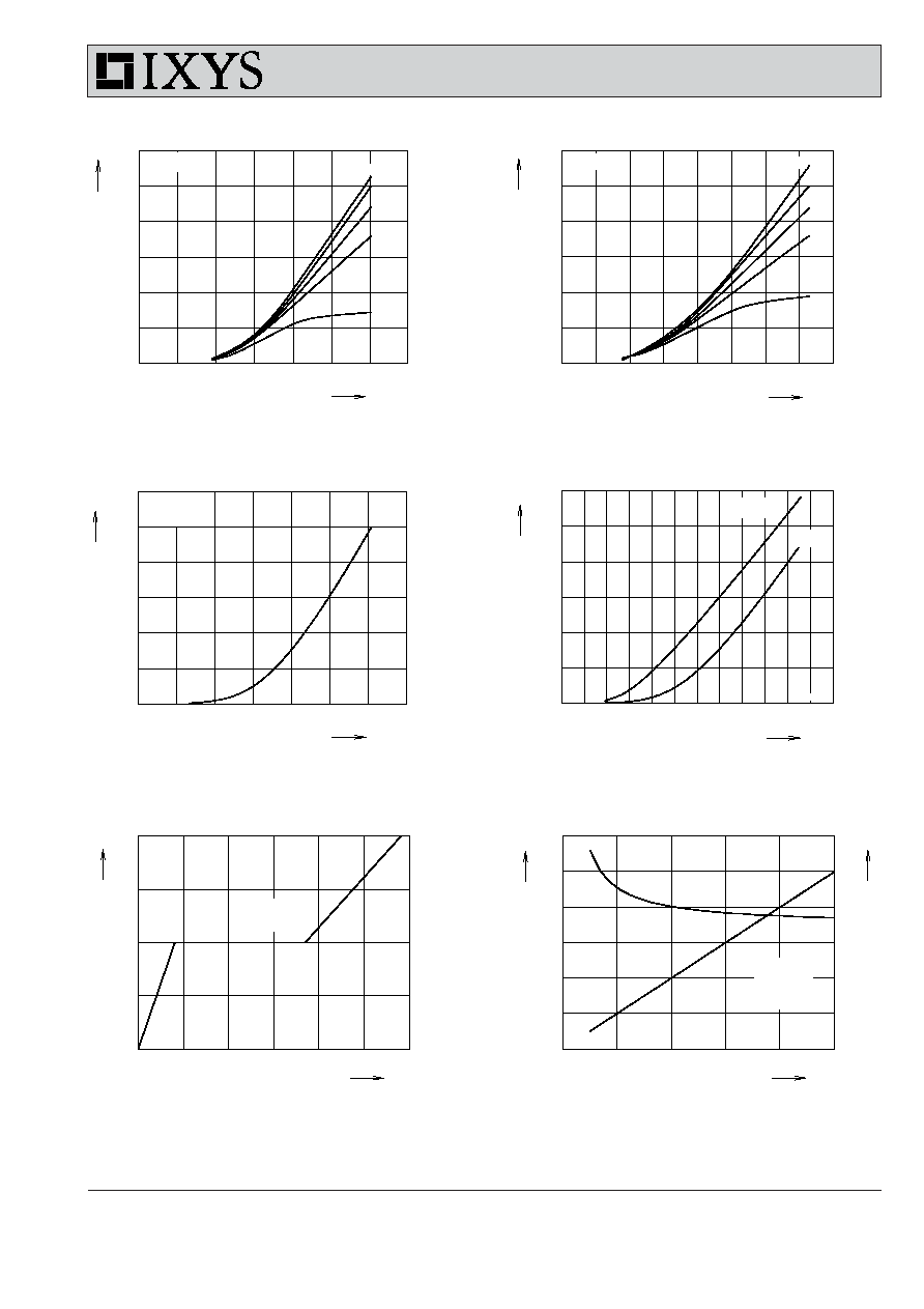
Fig. 1 Typ. output characteristics
Fig. 2 Typ. output characteristics
Fig. 3 Typ. transfer characteristics
Fig. 4 Typ. forward characteristics of
free wheeling diode
Fig. 5 Typ. turn on gate charge
Fig. 6 Typ. turn off characteristics of
free wheeling diode
0,5
1,0
1,5
2,0
2,5
3,0
3,5
0
30
60
90
120
150
180
0
200
400
600
800
1000
0
40
80
120
0
100
200
300
0,0
0,5
1,0
1,5
2,0
2,5
3,0
0
20
40
60
80
100
120
0
50
100
150
200
250
0
5
10
15
20
0,0
0,5
1,0
1,5
2,0
2,5
3,0
3,5
0
20
40
60
80
100
120
13 V
11 V
T
J
= 25∞C
V
GE
=17 V
T
J
= 125∞C
15 V
5
6
7
8
9
10
11
0
20
40
60
80
100
120
13 V
11 V
V
GE
=17 V
15 V
V
CE
= 20 V
T
J
= 25∞C
9 V
9 V
V
CE
V
A
I
C
V
CE
A
I
C
V
V
V
V
GE
V
F
A
I
C
A
I
F
nC
Q
G
-di/dt
V
V
GE
A
I
RM
t
rr
ns
A/
µ
s
T
J
= 125∞C
V
R
= 600 V
I
F
= 50 A
T
J
= 25∞C
I
RM
t
rr
81T120
81T120
81T120
81T120
81T120
V
CE
= 600 V
I
C
= 50 A
T
J
= 125∞C
DWLP55-12
© 2003 IXYS All rights reserved
4 - 4
IXYS reserves the right to change limits, test conditions and dimensions.
VDI
75-12P1 VII
75-12P1
VID
75-12P1 VIO
75-12P1
303
B3
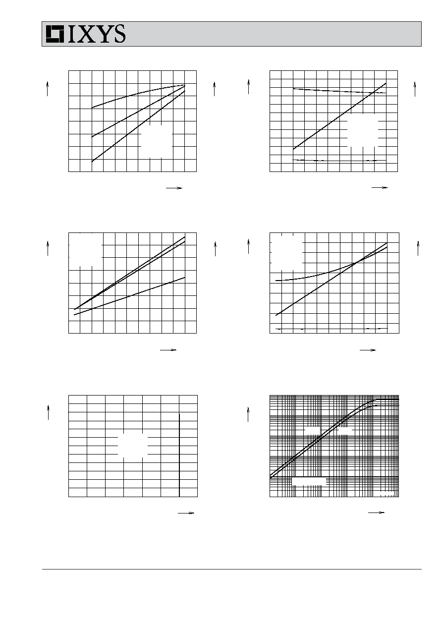
Fig. 7 Typ. turn on energy and switching
Fig. 8 Typ. turn off energy and switching
times versus collector current
times
versus collector current
Fig. 9 Typ. turn on energy and switching
Fig. 10 Typ. turn off energy and switching
times versus gate resistor
times
versus gate resistor
Fig. 11 Reverse biased safe operating area
Fig. 12
Typ. transient thermal impedance
RBSOA
0
20
40
60
80
100
0
6
12
18
24
0
30
60
90
120
0
20
40
60
80
100
0
2
4
6
8
10
12
0
100
200
300
400
500
600
0,00001 0,0001
0,001
0,01
0,1
1
0,00001
0,0001
0,001
0,01
0,1
1
0
10 20 30 40 50 60 70 80 90 100
0
2
4
6
8
10
0
300
600
900
1200
1500
0
10 20 30 40 50 60 70 80 90 100
0
5
10
15
20
0
60
120
180
240
single pulse
V
CE
= 600 V
V
GE
= ±15 V
I
C
= 50 A
T
J
= 125∞C
0
200
400
600
800 1000 1200
0
20
40
60
80
100
120
R
G
= 22
T
J
= 125∞C
V
CEK
< V
CES
E
on
t
d(on)
t
r
E
off
t
d(off)
t
f
E
on
t
d(on)
t
r
E
off
t
d(off)
t
f
I
C
A
I
C
A
mJ
E
off
mJ
E
on
ns
t
ns
t
R
G
R
G
V
CE
t
s
mJ
E
on
mJ
E
off
ns
t
ns
t
I
CM
K/W
Z
thJC
IGBT
diode
A
V
81T120
81T120
81T120
81T120
81T120
V
CE
= 600 V
V
GE
= ±15 V
R
G
= 22
T
J
= 125∞C
V
CE
= 600 V
V
GE
= ±15 V
R
G
= 22
T
J
= 125∞C
V
CE
= 600 V
V
GE
= ±15 V
I
C
= 50 A
T
J
= 125∞C
VID...75-12P1