
© 2003 IXYS All rights reserved
1 - 4
326
VUB 72
IXYS reserves the right to change limits, test conditions and dimensions.
Features
∑ three phase mains rectifier
∑ brake chopper:
- IGBT with low saturation voltage
- HiPerFRED
TM
free wheeling diode
∑ module package:
- high level of integration
- solder terminals for PCB mounting
- UL registered E72873
- isolated DCB ceramic base plate
- large creepage and strike distances
- high reliability
Applications
drives with
∑ mains input
∑ DC link
∑ inverter or chopper feeding the machine
∑ motor and generator/brake operation
V
RRM
= 1200/1600 V
I
dAVM
= 110 A
Three Phase Rectifier Bridge
with Brake Chopper
Input Rectifier D1 - D6
Symbol
Conditions
Maximum Ratings
V
RRM
VUB 72 -12 NO1
1200
V
VUB 72 -16 NO1
1600
V
I
FAV
T
C
= 80įC; sine 180į
40
A
I
DAVM
T
C
= 80įC; rectangular; d =
1
/
3
; bridge
110
A
I
FSM
T
VJ
= 25įC; t = 10 ms; sine 50 Hz
530
A
P
tot
T
C
= 25įC
100
W
Symbol
Conditions
Characteristic Values
(T
VJ
= 25
įC, unless otherwise specified)
min.
typ.
max.
V
F
I
F
= 25 A;
T
VJ
= 25įC
1.0
1.1
V
T
VJ
= 125įC
0.9
V
I
R
V
R
= V
RRM
;
T
VJ
= 25įC
0.02
mA
V
R
= 0.8
∑
V
RRM
; T
VJ
= 125įC
0.4
mA
R
thJC
per diode
1.2 K/W
R
thJH
with heat transfer paste
1.42 K/W
Chopper Diode D
Symbol
Conditions
Maximum Ratings
V
RRM
T
VJ
= 25įC to 150įC
1200
V
I
F25
DC; T
C
= 25įC
25
A
I
F80
DC; T
C
= 80įC
15
A
Symbol
Conditions
Characteristic Values
min.
typ.
max.
V
F
I
F
= 25 A; T
VJ
= 25įC
2.7
3.1
V
T
VJ
= 125įC
2.0
V
I
R
V
R
= V
RRM
;
T
VJ
= 25įC
0.1
mA
T
VJ
= 125įC
0.1
mA
I
RM
I
F
= 15A; di
F
/dt = -400 A/Ķs; T
VJ
= 125įC
16
A
t
rr
V
R
= 600 V
130
ns
R
thJC
2.3 K/W
R
thJH
with heat transfer paste
3.12 K/W
NTC
D1
D3
D5
D2
D4
D6
D
T
1 2
4 5
6
7
9 10
© 2003 IXYS All rights reserved
2 - 4
326
VUB 72
Chopper Transistor T
Symbol
Conditions
Maximum Ratings
V
CES
T
VJ
= 25įC to 150įC
1200
V
V
GES
Ī 20
V
I
C25
DC; T
C
= 25įC
50
A
I
C80
DC; T
C
= 80įC
35
A
I
CM
V
GE
=
Ī15 V; R
G
= 39
; T
VJ
= 125įC
50
A
V
CEK
RBSOA; L = 100 ĶH
V
CES
t
SC
V
GE
=
Ī15 V; V
CE
= 900 V; T
VJ
= 125įC
10
Ķs
(SCSOA)
R
G
= 39
; non repetitive
Symbol
Conditions
Characteristic Values
(T
VJ
= 25
įC, unless otherwise specified)
min.
typ.
max.
V
CE(sat)
I
C
= 25 A; V
GE
= 15 V; T
VJ
= 25įC
1.9
2.4
V
T
VJ
= 125įC
2.1
V
V
GE(th)
I
C
= 1 mA; V
GE
= V
CE
4.5
6.5
V
I
CES
V
CE
= V
CES
;
V
GE
= 0 V; T
VJ
= 25įC
0.1
mA
T
VJ
= 125įC
0.1
mA
I
GES
V
CE
= 0 V; V
GE
=
Ī 20 V
200
nA
t
d(on)
80
ns
t
r
50
ns
t
d(off)
440
ns
t
f
50
ns
E
on
3.8
mJ
E
off
2.0
mJ
C
ies
V
CE
= 25 V; V
GE
= 0 V; f = 1 MHz
2.0
nF
Q
Gon
V
CE
= 600 V; V
GE
= 15 V; I
C
= 25 A
250
nC
R
thJC
0.6 K/W
R
thJH
with heat transfer paste, see mounting instructions
1.2 K/W
Inductive load, T
VJ
= 125įC
V
CE
= 600 V; I
C
= 25 A
V
GE
= Ī15 V; R
G
= 39
Module
Symbol
Conditions
Maximum Ratings
I
RMS
per pin
100
A
T
VJ
-40...+150
įC
T
stg
-40...+125
įC
V
ISOL
I
ISOL
1 mA; 50/60 Hz; t = 1 min
3600
V~
M
d
Mounting torque (M5)
2 - 2.5
Nm
Symbol
Conditions
Characteristic Values
min.
typ.
max.
d
A
, d
S
5
mm
Weight
35
g
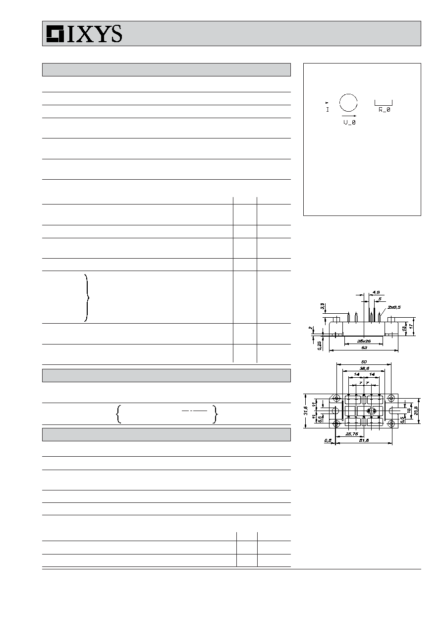
Equivalent Circuits for Simulation
Conduction
D1 - D6
Diode (typ. at T
J
= 125įC)
V
0
= 0.85 V; R
0
= 7 m
T/D
IGBT (typ. at V
GE
= 15 V; T
J
= 125įC)
V
0
= 1.0 V; R
0
= 45 m
Free Wheeling Diode (typ. at T
J
= 125įC)
V
0
= 1.25 V; R
0
= 32 m
Dimensions in mm (1 mm = 0.0394")
Temperature Sensor NTC
Symbol
Conditions
Characteristic Values
typ.
R
25
T = 25įC
2.2
k
B
25/100
100
K
R(T) = R
25
∑ eB
25/100
1
1
T
298K
(
)
© 2003 IXYS All rights reserved
3 - 4
326
VUB 72
0
10
20
30
40
50
60
70
0
20
40
60
80
100
120
140
P
tot
I
d(AV)M
A
W
T
A
0
40
80
120
160
įC
R
thHA
[K/W]
0.5
1
1.5
2
3
4
6
0.0
0.5
1.0
1.5
2.0
0
10
20
30
40
50
60
70
80
V
F
A
I
F
V
T
VJ
= 25
įC
T
VJ
=150įC
max.
typ.
0
40
80
120
160
0
10
20
30
40
50
60
70
80
T
H
I
d(AV)M
įC
A
I
2
t
A
2
s
ms
t
1
10
10
100
1000
10000
T
VJ
= 150
įC
T
VJ
= 45
įC
V
R
= 0 V
s
t
A
I
FSM
0.001
0.01
0.1
1
0
100
200
300
400
500
V
R
= 0.8V
RRM
T
VJ
= 45
įC
T
VJ
= 150
įC
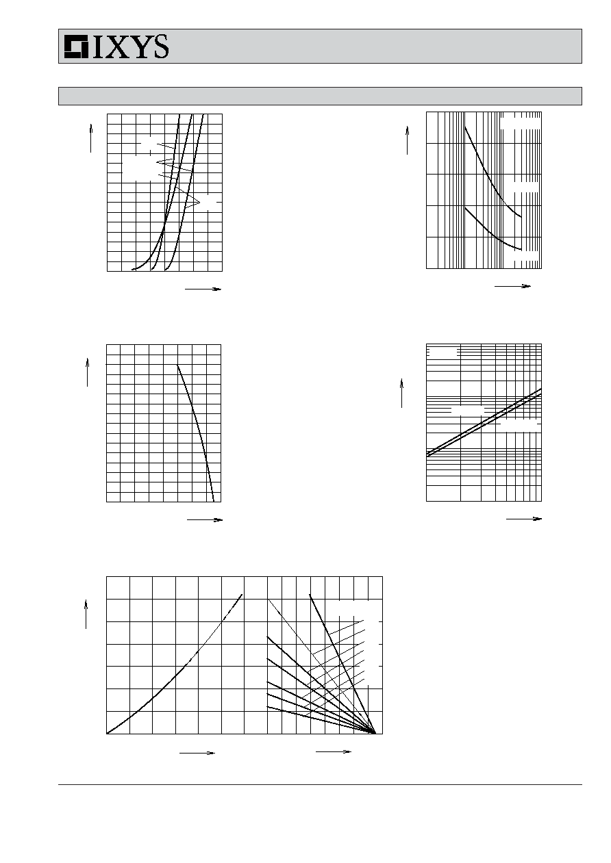
Input Rectifier D1-D6
Fig. 3 Maximum forward current
Fig. 4 I2t versus time
versus heatsink temperature (Rectifier bridge)
per rectifier diode
Fig. 5
Power dissipation versus direct output current and ambient temperature (Rectifier bridge)
Fig. 1 Forward current versus voltage
Fig. 2 Surge overload current per
drop per rectifier diode
rectifier diode
Note:
transient thermal impedance
see next page
© 2003 IXYS All rights reserved
4 - 4
326
VUB 72
0
1
2
3
4
5
6
7
0
20
40
60
80
100
120
V
V
CE
A
I
C
0
1
2
3
4
0
10
20
30
40
50
V
V
F
I
F
A
0
20
40
60
80
0
2
4
6
0
200
400
600
800
1000
1200
E
off
t
d(off)
t
f
I
C
A
E
off
t
mJ
ns
10
20
30
40
50
60
70
80
0
1
2
3
4
0
200
400
600
800
E
off
t
d(off)
t
f
E
off
t
ns
mJ
0.00001 0.0001
0.001
0.01
0.1
1
10
0.0001
0.001
0.01
0.1
1
10
t
s
K/W
Z
thJC
0
25
50
75
100
125
150
1900
2000
2100
2200
2300
T
įC
R
R
G
V
GE
= 15 V
T
VJ
= 125įC
T
VJ
= 25įC
single pulse
T
VJ
= 25įC
T
VJ
= 125įC
V
CE
= 600 V
V
GE
= Ī15 V
R
G
= 39
T
VJ
= 125įC
V
CE
= 600 V
V
GE
= Ī15 V
I
C
= 35 A
T
VJ
= 125įC
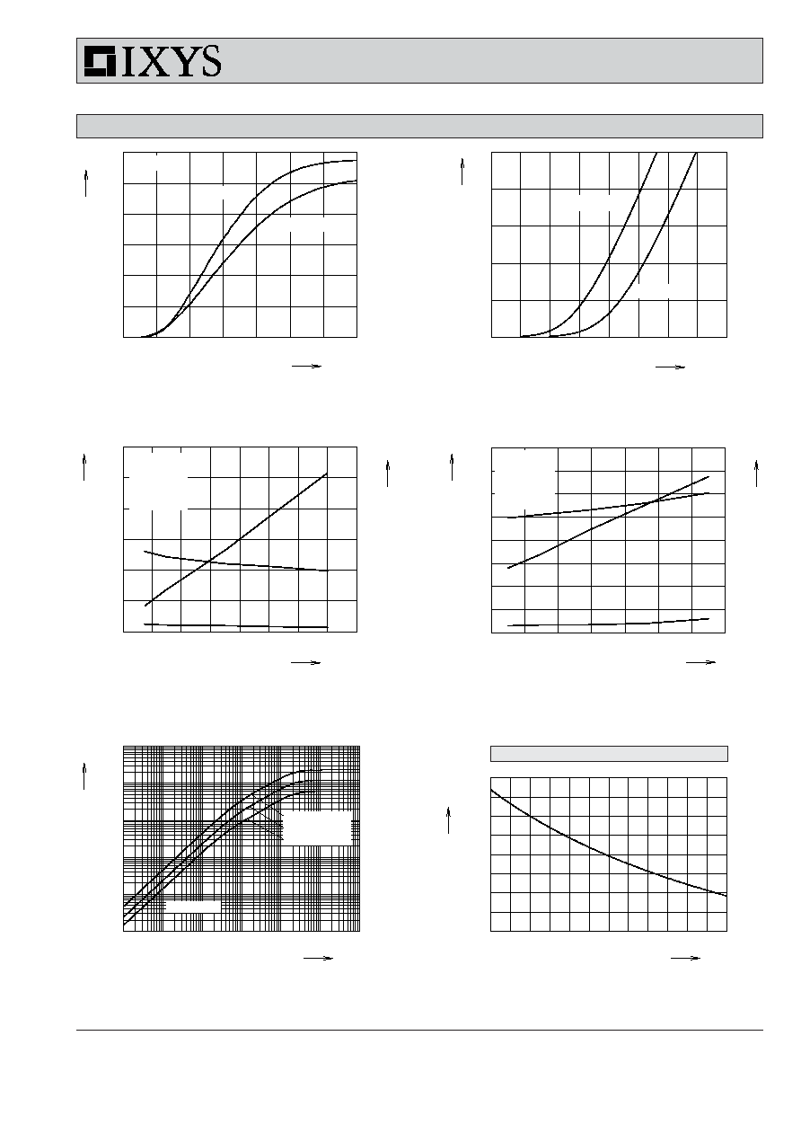
chopper diode
rectifier diode
IGBT
Fig. 6 Typ. IGBT output characteristics
Fig. 7 Typ. forward characteristics
of free wheeling diode
Fig. 8 Typ. IGBT turn off energy and switching
Fig. 9 Typ. IGBT turn off energy and switching
times versus collector current
times versus gate resistor
Fig. 10
Typ. transient thermal impedance
Fig. 11
Typ. thermistorresistance versus
temperature
Temperature Sensor NTC
Chopper T - D