
HE11020F
Confidential
2001 / 7 / 17
version 0.96
1
USB to ATA/ATAPI/SD/MMC Interface
Controller
1 General Description
This chip provides a high-performance interface to bridge USB and ATA/ATAPI/SD/MMC compliance
device, therefore, it could be used to connect IDE hard disk, CD-ROM, CD-RW, Compact Flash card, MMC or SD
memory card. It provides a flexible and low cost single chip solution for applications intended to utilize the convenience
of USB. The maximum supported serial clock in SD/MMC interface is 12MHz and the supported block length is 2048
bytes. The external serial EEPROM gives users the possibility to customize their USB identity, i.e., the user could
modify the vendor ID and product ID for various version of products and stores them in the external EEPROM.
2 Features
USB 1.1 compatible.
Support ATA/ATAPI, PIO mode
SD memory card specification 1.0 compatible.
MMC memory card specification 2.1.1 compatible.
SD/MMC serial clock rate is up to 12MHz.
Built-in FIFO for upstream and downstream data transfer.
Pin selectable bus-power or self-power.
Eight user-defined general purpose IO.
Drivers support Microsoft Windows 98/Windows 2000/Mac
Single 3.3V operation in 80-pin LQFP package.
3. Pin Assignment
3.1 LQFP80 package

HE11020F
Confidential
2001 / 7 / 17
version 0.96
2
Pin# Pin Name
Type
Drive
Special
Description
1
VSS
P
-
-
3.3V digital power ground
2
RSTN
DI
ST, PU
Bridge reset (internal pull-up)
3
TEST
DI
ST, PD
Test pin
4
SELPWR
DI
ST, PD
Power select pin; 0: Bus power 1: self power
5
GPIO0
DIO
8mA
ST, SR
General purpose input/output
6
GPIO1
DIO
8mA
ST, SR
General purpose input/output
7
GPIO2
DIO
8mA
ST, SR
General purpose input/output
8
GPIO3
DIO
8mA
ST, SR
General purpose input/output;
Input also used as USB wakeup
9
ATANIOR
DO
8mA
SR
APAPI I/O read signal, active low
10
NC
-
-
-
No connected
11
NC
-
-
-
No connected
12
ATANIOW
DO
8mA
SR
ATAPI I/O write signal, active low
13
ATADD3
DIO
8mA
TTL, SR
ATA data bit3
14
ATADD11
DIO
8mA
TTL, SR
ATA data bit11
15
ATADD4
DIO
8mA
TTL, SR
ATA data bit4
16
ATADD12
DIO
8mA
TTL, SR
ATA data bit12
17
ATADD5
DIO
8mA
TTL, SR
ATA data bit5
18
ATADD13
DIO
8mA
TTL, SR
ATA data bit13
19
ATADD6
DIO
8mA
TTL, SR
ATA data bit6
20
VSS
P
-
-
3.3V digital power ground
21
NC
-
-
-
No connected
22
VDD
P
-
-
3.3V digital power supply
23
XVDD
P
-
-
Oscillator power supply
24
XIN
I
-
-
Crystal input or oscillator input
25
XOUT
O
-
-
Crystal input or no connection
26
XVSS
P
-
-
Oscillator power ground
27
ATADD14
DIO
8mA
TTL, SR
ATA data bit14
28
ATADD7
DIO
8mA
TTL, SR
ATA data bit7
29
VSS
P
-
-
3.3V digital power ground
30
ATADD15
DIO
8mA
TTL, SR
ATA data bit 15
31
NC
-
-
-
No connected
32
ATADD0
DIO
8mA
TTL, SR
ATA data bit 0
33
ATADD1
DIO
8mA
TTL, SR
ATA data bit 1
34
ATADD8
DIO
8mA
TTL, SR
ATA data bit 8
35
ATADD2
DIO
8mA
TTL, SR
ATA data bit 2
36
ATADD9
DIO
8mA
TTL, SR
ATA data bit 9
37
ATADD10
DIO
8mA
TTL, SR
ATA data bit 10
38
ATACS0
DO
8mA
SR
ATAPI chip select 0
39
VDD
P
-
-
3.3V digital power supply
40
NC
-
-
-
No connected
41
VSS
P
-
-
3.3V digital power ground
42
ATACS1
DO
8mA
SR
ATAPI chip select 1
43
ATADA2
DO
8mA
SR
ATAPI device address 2
44
ATADA1
DO
8mA
SR
ATAPI device address 1
45
ATADA0
DO
8mA
SR
ATAPI device address 0
46
ATARSTN
DO
8mA
TTL, ST
ATA reset, active low
47
ATAIRDY
DI
-
TTL, ST
ATAPI data ready signal, active high
48
ATAINTR
DI
-
TTL, ST
ATA interrupt request
49
VDD
P
-
-
3.3V digital power supply
50
ROMDO
DI
-
ST
Serial data from external EEPROM
51
NC
-
-
-
No connected
52
NC
-
-
-
No connected
53
ROMSK
DO
4mA
SR
Clock for external serial EEPROM
54
ROMCS
DO
4mA
SR,
Chip select for external EEPROM
55
SDDIO0
DIO
8mA
SR, ST
SD/MMC data 0
HE11020F
Confidential
2001 / 7 / 17
version 0.96
3
56
SDDIO1/ROMDI
DIO
8mA
SR, ST
SD data 1/serial data to external EEPROM
57
SDDIO2
DIO
8mA
SR, ST
SD data 2
58
SDDIO3
DIO
8mA
SR, ST
SD data 3
59
SDCMD
DIO
8mA
SR, ST
SD/MMC command
60
VSS
P
-
-
3.3V digital power ground
61
VDD
P
-
-
3.3V digital power supply
62
SDCLK
DO
8mA
SR
SD/MMC bus clock
63
PWRSW
DO
8mA
SR
Power down control
64
GPIO4
DIO
8mA
ST, SR
General purpose input/output
65
GPIO5
DIO
8mA
ST, SR
General purpose input/output
66
GPIO6
DIO
8mA
ST, SR
General purpose input/output; for SD, it is the
write-protect pin
67
GPIO7
DIO
8mA
ST, SR
General purpose in/output; for SD, it is the card-
detect pin
68
VSS
P
-
-
3.3V digital power ground
69
TAVDD
P
-
-
USB transceiver power supply
70
DPLUS
AIO
-
-
USB D+ signal
71
NC
-
-
-
No connected
72
NC
-
-
-
No connected
73
NC
-
-
-
No connected
74
DMINUS
AIO
-
-
USB D- signal
75
TAVSS
P
-
-
USB transceiver power ground
76
AVSS
P
-
-
On-chip PLL power ground
77
AVDD
P
-
-
On-chip PLL power supply
78
VDD
P
-
-
3.3V digital power supply
79
NC
-
-
-
No connected
80
NC
-
-
-
No connected
P: power pin; AI: analog input pin, AIO: analog input/output pin; DI: digital input pin; DO: digital output pin; DIO:
digital input/output pin.
TTL: TTL compatible input pin; ST: schmit trigger pad, PD: pull down; PU: pull up; SR: slew rate control.
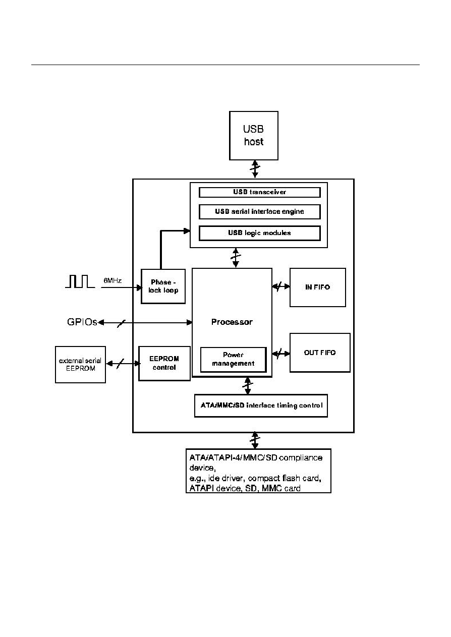
4. Block Diagram
HE11020F
Confidential
2001 / 7 / 17
version 0.96
4
4. Block Diagram
HE11020F
Confidential
2001 / 7 / 17
version 0.96
5
5. Operating Description
5.1 USB Descriptor
This bridge supports one device descriptor with one configuration and one interface. There are three endpoints within the
interface. Endpoint 0 is the default control endpoint. Endpoint 1 is the Bulk-in endpoint ( data from device to host ) and
endpoint 2 is the Bulk-out endpoint ( data from host to device ).
5.1.1 Device Descriptor
Offset
Field
Size
Value
Descriptor
0
blength
Byte
12H
Size of this descriptor in byte
1
bdescriptor Type
Byte
01H
DEVICE descriptor type
2
bcdUSB
Word
0110H
USB specification version 1.1
4
bdevice Class
Byte
00H
Interface specific
5
bdevice SubClass
Byte
00H
Interface specific
6
bdevice Protocol
Byte
00H
Interface specific
7
bmax Packet Size
Byte
40H
Maximum packet size for endpoint zero is 64
8
idVendor
Word Note 7 . 1 . 1 Vendor ID
10
idProduct
Word Note 7 . 1 . 1 Product ID
12
bdc Device
Word
0100H
Device release 1.0
14
imanufacture
Byte
00H
Null
15
iproduct
Byte
00H
Null
16
Iserial Number
Byte
00H
Null
17
bnum Configurations
Byte
01H
One possible configuration
Note 7 . 1 . 1 : These values depends on the external EEPROM and the GPIO configuration.
5.1.2 Configuration Descriptor
Offset
Field
Size
Value
Descriptor
0
bLength
Byte
09H
Size of this descriptor in bytes
1
bDescriptor
Byte
02H
CONFIGURATION descriptor type
2
bTotalLength
Word
0020H
4
bNumInterface
Byte
01H
The bridge has one interface
5
bConfiguration Value
Byte
01H
6
iConfiguration
Byte
00H
Null
7
bmAttributes
Byte
E0H / A0H
Bus / self powered ; depends on PWRSEL. For Bus
power : A0H, For Self power: E0H
8
MaxPower
Byte
32H / FAH
Depends on PWRSEL, for Bus power : FAH, for self
power : 32H